Article

Towards the Development of Electrical Biosensors Based on Nanostructured Porous Silicon

Departamento de Física Aplicada and Centro de Investigaciones Biomédicas en Red; Biomateriales, Bioingeniería y Nanomedicina (CIBERbbn), Universidad Autónoma de Madrid, 29049 Cantoblanco, Madrid, Spain
*
Author to whom correspondence should be addressed.
Materials 2010, 3(2), 755-763; https://doi.org/10.3390/ma3020755
Submission received: 14 December 2009 / Revised: 12 January 2010 / Accepted: 25 January 2010 / Published: 27 January 2010
(This article belongs to the Special Issue Porous Materials)

Abstract

:
The typical large specific surface area and high reactivity of nanostructured porous silicon (nanoPS) make this material very suitable for the development of sensors. Moreover, its biocompatibility and biodegradability opens the way to the development of biosensors. As such, in this work the use of nanoPS in the field of electrical biosensing is explored. More specifically, nanoPS-based devices with Al/nanoPS/Al and Au-NiCr/nanoPS/Au-NiCr structures were fabricated for the electrical detection of glucose and Escherichia Coli bacteria at different concentrations. The experimental results show that the current-voltage characteristics of these symmetric metal/nanoPS/metal structures strongly depend on the presence/absence and concentration of species immobilized on the surface.

Graphical Abstract

1. Introduction

The particular structure and surface morphology of nanostructured porous silicon (nanoPS), as well as the properties of the nanoPS/Si interface, together with the relatively good control over its physicochemical behavior provided by electrochemical processes, has stimulated much research leading to many different applications in a number of fields ranging from microelectronics to biomedical applications. A number of examples can be found in references [1,2,3]. It is worth noting that the nanoPS formation process is fully compatible with current semiconductor processing technologies.
NanoPS can be regarded as a complex network of silicon nanocrystals embedded into a porous matrix [4,5,6]. The large specific surface area of nanoPS together with its large surface reactivity allows the fabrication, among other devices, of chemical sensors and biosensors. In particular, the electrical behavior of nanoPS is in general extremely sensitive to its surface properties and composition [7,8,9], and is highly sensitive to the presence or absence of biomolecules on its surface [10]. Therefore, the integration of nanoPS in electrical biosensors would result in increased sensitivity.
Moreover, its particular surface structure and large specific surface is highly attractive for the nucleation of bioceramic apatite in simulated body fluids [11] and can be used as a catalytic environment for protein nucleation [12]. An additional advantage is given by the fact that for some specific applications no surface functionalization is required for the subsequent covalent linkage of biomolecules.
In this work, nanoPS-based devices with a metal/nanoPS/metal structure were fabricated for the electrical detection of glucose and Escherichia coli (E. coli). Immobilization of glucose on nanoPS was successfully performed with no previous surface functionalization. However, biofunctionalization was required for the immobilization of E. coli fragments for subsequent detection. Based on our previous experience [13,14,15], biofuntionalization of nanoPS was performed by the use of solutions of aminopropyltriethoxysilane (APTS) in toluene. These solutions were found to be highly adapted for the subsequent immobilization of E. coli antibodies through the high density of amino groups induced on the surface of nanoPS. After antibody immobilization, fragments of E. coli, which are specifically recognized by the antibodies present on the surface of nanoPS, were immobilized. The nanoPS-based devices were found to show a strong dependence of their electrical behavior on the presence and concentration of glucose and E. coli fragments.

2. Experimental

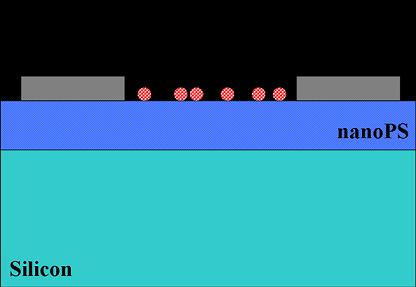
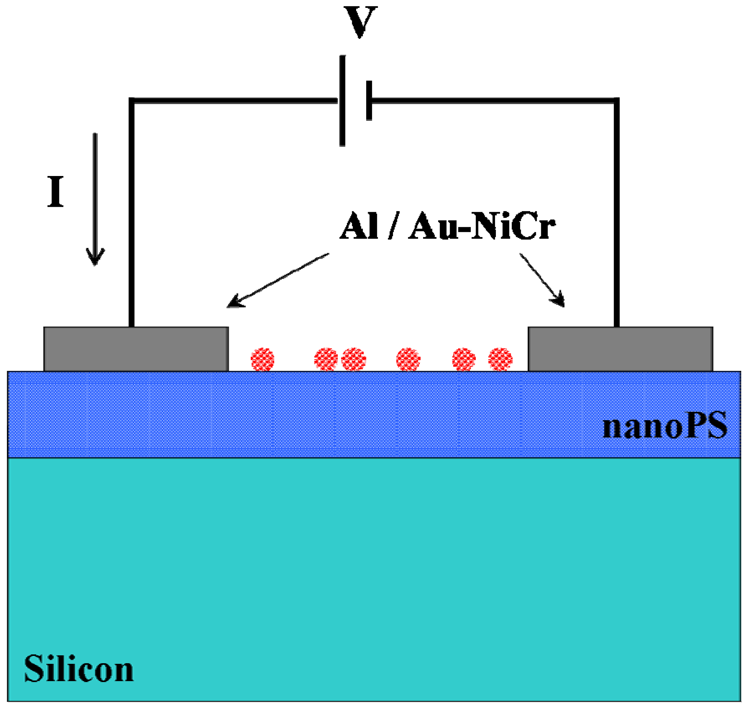
2.1. Fabrication of Electrical Biosensors Based on Nanostructured Porous Silicon

Layers of nanoPS were grown by electrochemical etching of boron-doped (p-type) silicon wafers (orientation: <100>, resistivity: 0.1–0.5 Ωcm). Low resistivity ohmic contacts were formed by coating the backside of the Si wafers with Al and subsequently annealing at 400 °C for 5 min. The wafers were cut into 1×1 cm2 pieces which were mounted into a sample holder with an exposed area to the electrochemical etching solution of 0.64 cm2. The electrolyte consisted of HF (48 wt %):ethanol (98 wt %) solutions with different HF to ethanol ratios. The wafers were galvanostatically etched using etching current densities ranging from 10 mA/cm2 to 100 mA/cm2, and etching times from 20 to 180 seconds. Illumination from a 100 W halogen lamp was used to promote the generation of electron-hole pairs, this contributing to reduce the typical crystallite size.
Metal (Al or Au-NiCr) top contacts were used as 1-mm-diameter diode pads for the fabrication of the electrical biosensors. Since Au often does not adhere well to the surface of nanoPS, extremely thin NiCr layers (~10 Ǻ) were previously sputter-deposited onto the nanoPS layers. The overall process leads to two different biosensing structures: Al/nanoPS/Al and Au-NiCr/nanoPS/Au-NiCr. Figure 1 shows the structure of the nanoPS-based devices used for the electrical biosensing of glucose and E. Coli fragments.
Figure 1. Cross-sectional view of a typical metal/nanoPS/metal biosensing device and configuration used for the electrical characterization.
Materials 03 00755 g001

2.2. Immobilization of Glucose

NanoPS-based devices with the structure Al/nanoPS/Al were incubated with glucose (D-(+)-glucose, Sigma-Aldrich). As such, glucose was diluted in distilled water at different concentrations ranging from 1 μg/L to 1000 μg/L. The nanoPS-based devices were incubated in 2 mL glucose solutions for 20 minutes. Removal of non-adsorbed glucose molecules was accomplished by the immersion of the samples in 2 mL of water for five minutes. This process was repeated twice to ensure effective removal of non-adsorbed glucose molecules.

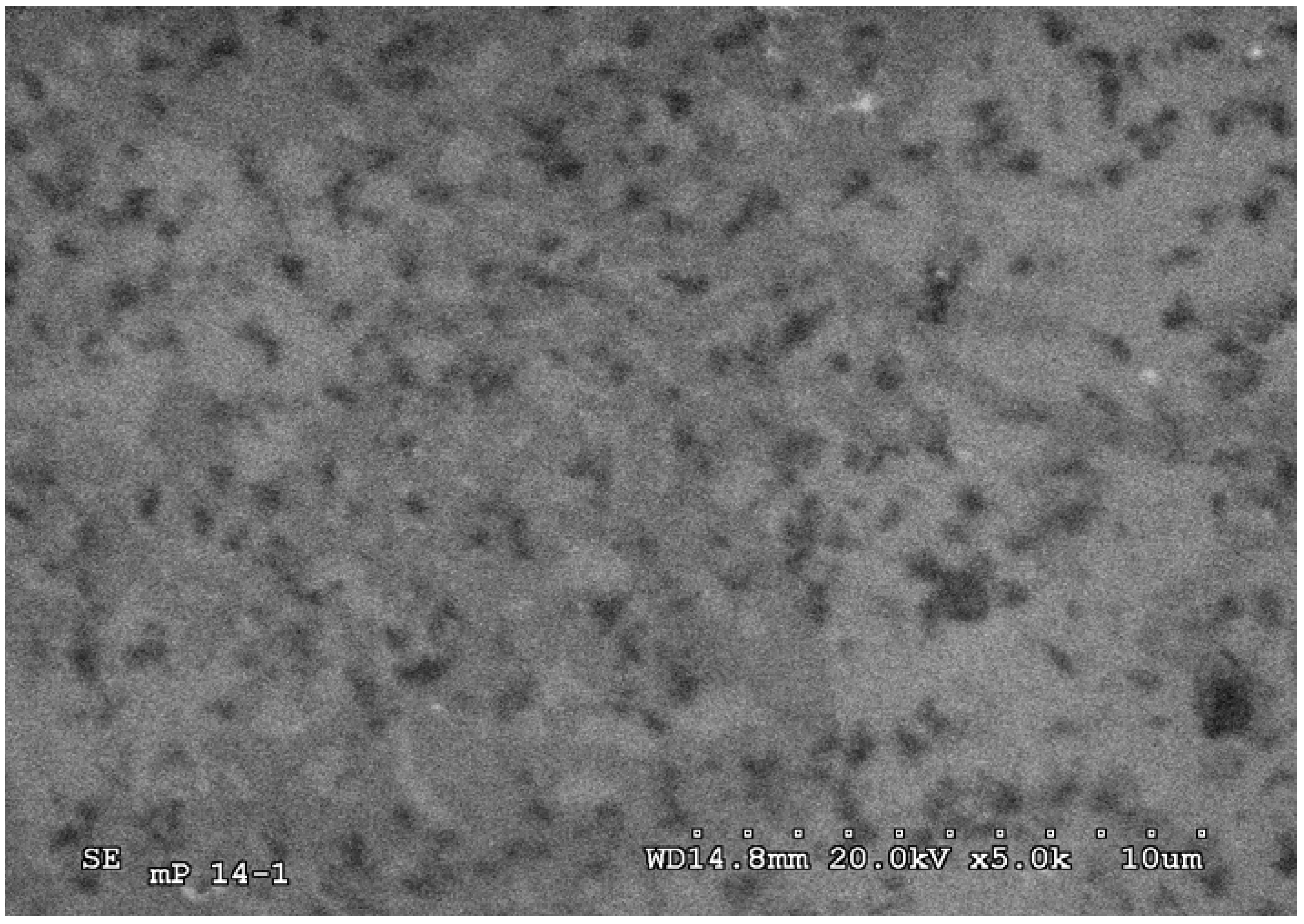
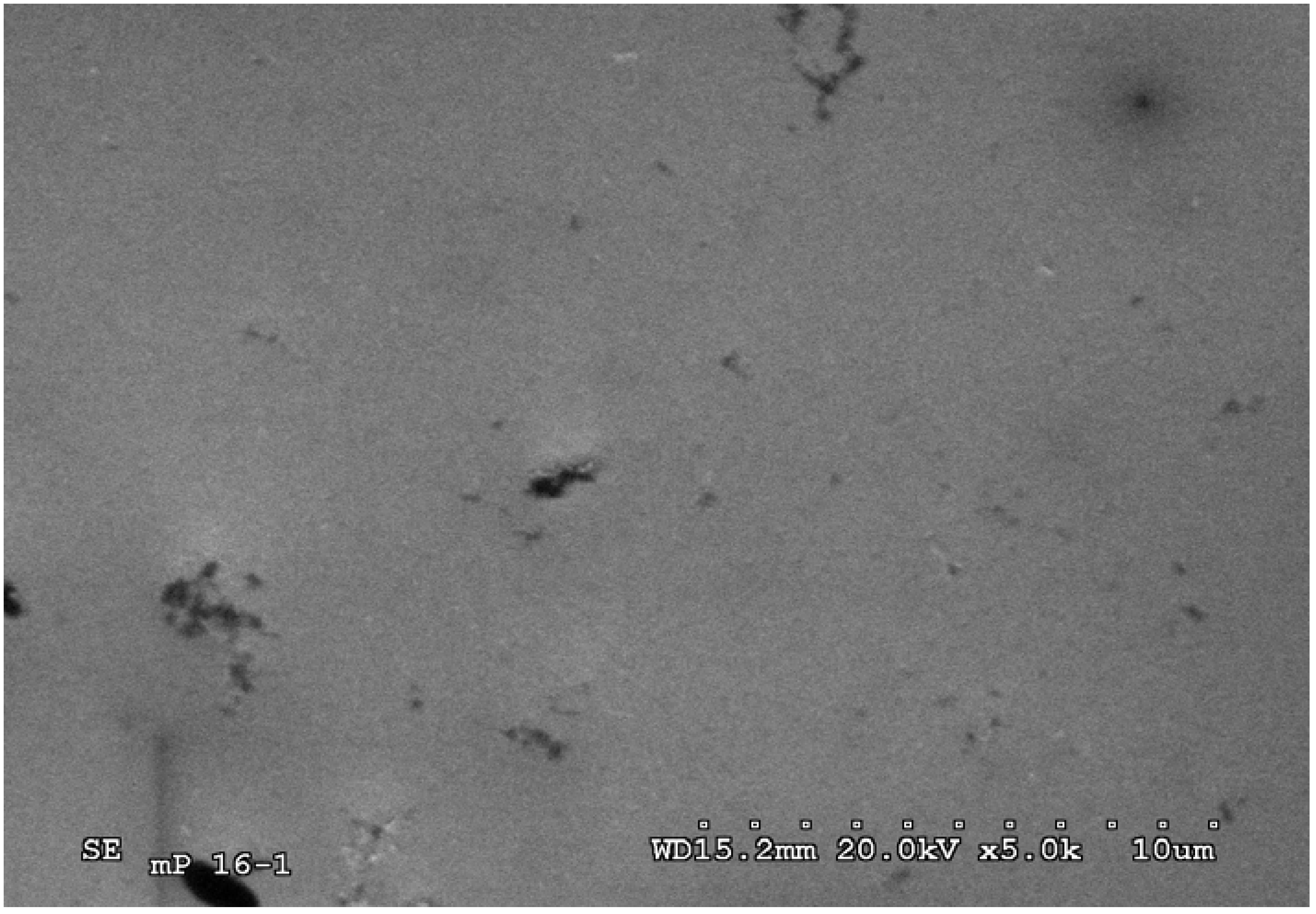
2.3. Biofunctionalization and Immobilization of E. Coli

Aiming at the subsequent immobilization of E. coli antibodies, surface biofuntionalization was performed by the immersion of the nanoPS-based devices in aminopropyltriethoxysilane (APTS)-toluene (2:1,000) solutions for 15 min. Amine groups were chosen since they are present in proteins, and their chemical interaction with other functional groups is relatively well understood. Furthermore, APTS has been previously demonstrated to allow the effective surface functionalization of nanoPS [13,15]. In this process, the presence of SiO2 on the surface of nanoPS (formed by the oxidation as a result of exposure to ambient air), reacts with the APTS-based solution leading to a large surface density of amino groups.
E. coli antibodies (Abcam) were immobilized on the functionalized surface by the immersion of nanoPS-based devices with the structure Au-NiCr/nanoPS/Au-NiCr in antibody: phosphate buffered saline (PBS) 1x in a range of concentrations from 0 to 100 μg/mL. After antibody immobilization, E. coli fragments (KPL) were immobilized following the same procedure, i.e., by the immersion of the nanoPS-based devices in E. coli fragments: PBS solutions of different concentration (ranging from 2.5 to 100 μg/mL) for 30 minutes. Before and after each incubation step, the nanoPS-devices were rinsed in distilled water to eliminate any non surface linked antibodies or fragments and/or remaining PBS crystals.

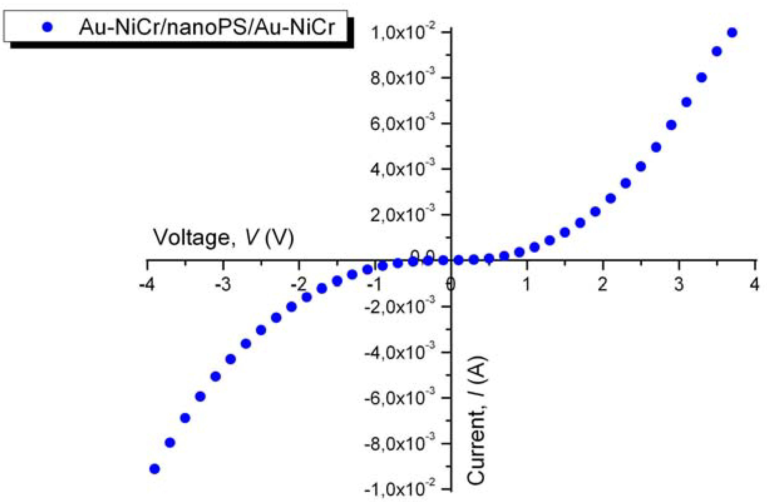
2.4. Electrical Characterization

Electrical characterization (I-V curves) was carried out in the dark by using a Hewlett Packard pA meter/dc voltage source, Model 4140B. Figure 1 shows the configuration used for the determination of the electrical behavior (I-V curves) of the nanoPS-based devices.

3. Results

Current-voltage measurements (I-V curves) were taken between two consecutive contacts deposited on top of the surface of nanoPS (Figure 1) immediately after the fabrication of the metal/nanoPS/metal devices. Figure 2 shows a typical I-V curve for the Au-NiCr/nanoPS/Au-NiCr devices, from which it is observed that these structures show a double rectifying behavior. A similar behavior has been previously observed in symmetrical nanoPS-based devices with the structure metal/nanoPS/Si/nanoPS/metal using differet metals (Au/Cr, W, Ta, WTi, Cr and Ti), finding that the current through the PS-based structures greatly depends on the metallic contact and that Au contacts with an extremely thin Cr underlayer provide the highest values of current [16].
Figure 2. Typical I-V curve for the Au-NiCr/nanoPS/Au-NiCr symmetrical structures.
Materials 03 00755 g002

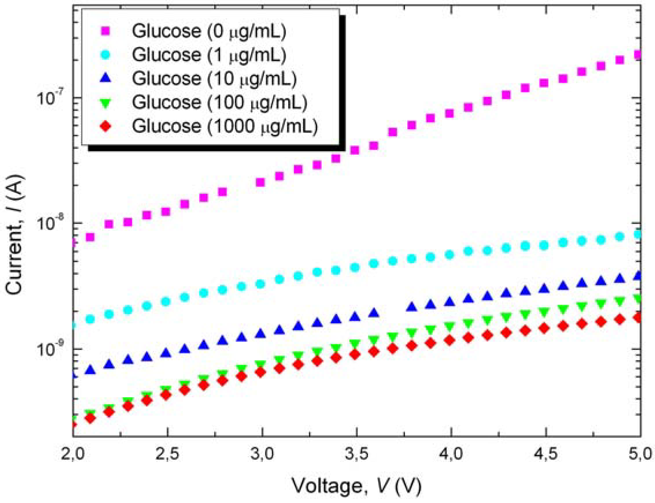
3.1. Electrical Biosensing of Glucose

The singular structure and composition of the surface of nanoPS has been demonstrated to favor immobilization of glucose [10]. Accordingly, for this particular application no previous surface functionalization is required. The large surface activity of nanoPS observed in this and previous works [15] can be partially attributed to its high specific surface which provides numerous available bonding sites, as a result of the electrochemical formation process in HF-based solutions and subsequent oxidation processes.
Typical current-voltage (I-V) characteristics acquired immediately after the immobilization of glucose on the surface of nanoPS are shown in Figure 3. It is notable that resistivity has noticeably increased, most likely due to surface oxidation of the porous structure. The different curves were recorded for several concentrations of glucose in distilled water, ranging from 0 μg/mL to 1,000 μg/mL. From Figure 3 it is observed that increasing glucose concentration results in lower current for a given voltage. Additionally, the horizontal distance between the curves is smaller for increasing glucose concentration, indicating that the devices are approaching the saturation limit. In particular, the curves corresponding to 100 μg/mL and 1,000 μg/mL practically overlap for low voltages.
Figure 3. Current (I) as a function of applied voltage (V) for Al/nanoPS/Al structures after glucose immobilization from solutions at different concentrations.
Materials 03 00755 g003
The experimental results indicate that the immobilization of glucose on the surface of nanoPS leads to changes in its surface charge distribution, resulting in lower conductivity through the Al/nanoPS/Al devices. These results agree with previously reported measurements of electrical conductivity of glucose in water [17]. Moreover, the reduction in conductance is not attributed to water used for the dissolution of glucose, since water has been previously demonstrated to increase the conductivity of nanoPS [18,19]. Accordingly, this effect has been attributed to changes in the dielectric constant, dipole moment and possible chemisorption or physioadsorption on the surface of nanostructured porous silicon.

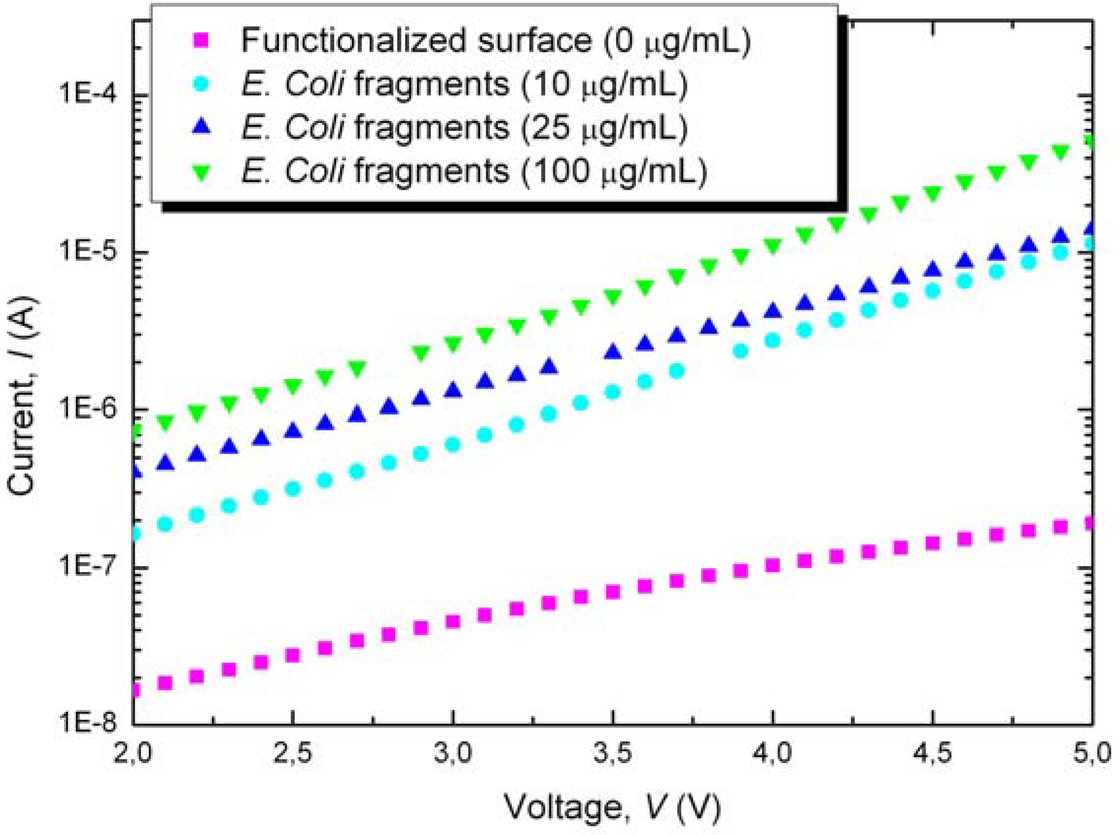
3.2. Electrical Biosensing of E. coli

As opposed to the case of glucose immobilization, biofunctionalization is required to provide a soft chemical binding layer for the subsequent immobilization of E. coli antibodies. The presence of reactive amine functional groups on the surface of functionalized nanoPS has been previously confirmed by X-ray photoelectron spectroscopy (XPS) characterization, from which it was determined that the main elements present in the surface of nanoPS are nitrogen, oxygen, silicon and carbon [13].
Electrical characterization was performed after surface biofunctionalization in APTS-toluene solutions, from which a double-rectifying behavior was again observed, as in the case of as-formed nanoPS-based devices. However, surface biofunctionalization results in decreased conductivity for a given voltage for both forward and reverse polarization. E. coli antibody immobilization was performed by incubation in E. coli antibody:PBS solutions at 25 μg/mL leading to increased conductivity. It was also determined that higher antibody concentration results in larger current for a given voltage.
The surface of nanoPS was analyzed by scanning electron microscopy (SEM) immediately after the biofunctionalization process and after the immobilization of fragments of bacterium E. coli (Figure 4). Surface analysis shows the successful immobilization of fragments of bacterium E. coli on the surface of nanoPS (Figure 4, bottom). As such, it was verified that the antibodies and fragments of bacterium have been linked to the nanostructured surface.
Figure 4. Scanning electron microscopy (SEM) images of the surface of nanoPS immediately after the biofuntionalization process (top), and after immobilization of antibodies (100 μg/mL) plus fragments of E. coli bacterium (bottom).
Materials 03 00755 g004aMaterials 03 00755 g004b
Finally, current-voltage measurements were performed after probing E. coli fragments on the Au-NiCr/nanoPS/Au-NiCr devices from PBS solutions of increasing concentration of E. coli fragments, ranging from 10 μg/mL to 100 μg/mL. Figure 5 shows the experimental results, from which increased conductivity is observed for increased E. coli fragment concentration. This suggests that the higher the concentration, the larger the surface concentration of E. coli fragments on the surface of nanoPS and hence the device is more conductive. In the range of concentrations used in this work no saturation effects were found.
Figure 5. Current (I) as function of the applied voltage (V) through the Au-NiCr/nanoPS/Au-NiCr structure after probing with E. coli fragments at different concentrations on devices with E. coli antibodies previously immobilized in 25 μg/mL solutions.
Materials 03 00755 g005
From the experimental results it can be inferred that the electrical behavior of devices with the Au-NiCr/nanoPS/Au-NiCr structure is greatly affected by the following three processes: funtionalization in APTS-toluene solution, immobilization of E. coli antibodies and probing with fragments of E. coli.
In particular, the funtionalization process results in decreased conductivity, which most likely has its origin in the presence of a large surface density of amino groups on the surface and near-surface of nanoPS. However, the immobilization of antibodies and fragments of E. coli leads to increased conductivity, suggesting that antibodies posses higher conductivity than nanoPS, and that they have successfully been linked to the biofuntionalized surface. In this respect, previous studies have determined the conductivity of colloidal E. coli particles of 1 micron in diameter to be 0.03 mho/m [20]. Additionally, increased conductivity suggests that the biomolecules might be not only present on the surface of nanoPS, but slight diffusion into the structure of nanoPS might have occurred. The variations on the conductivity are attributed, as in the case of glucose, to the effects caused by the immobilization of biomolecules in the dielectric constant and dipolar moments on the surface of nanoPS.

4. Conclusions

Electrical devices based on nanostructured porous silicon with the Al/nanoPS/Al and Au-NiCr/nanoPS/Au-NiCr structure were fabricated and characterized, showing a double rectifying behavior.
Glucose biomolecules were immobilized on the surface of nanoPS from solutions of glucose in distilled water at different concentrations. Electrical measurements (current-voltage characteristics) were performed through the nanoPS-based structures, from which a reduction of current for increasing glucose concentration (constant voltage) is observed.
Biofunctionalization was required for the subsequent immobilization of E. coli antibodies on the surface of nanoPS. However, the conductivity of the Au-NiCr/nanoPS/Au-NiCr devices is somewhat lowered by the biofunctionalization process. Finally, immobilization of antibodies and fragments of E. coli resulted in increased conductivity and showed a dependence on E. coli surface concentration. Accordingly, the Au-NiCr/nanoPS/Au-NiCr devices have been demonstrated as possible candidates for the subsequent development of biosensors for E. coli bacteria.

Acknowledgements

The authors thank L. García-Pelayo for technical support in the realization of this work.

References

  1. Lehmann, V. Electrochemistry of Silicon: Instrumentation, Science, Materials and Applications; Wiley-VCH: Weinheim, Germany, 2002. [Google Scholar]
  2. Föll, H.; Christophersen, M.; Carstensen, J.; Hasse, G. Formation and application of porous silicon. Mat. Sci. Eng. R 2002, 39, 93–141. [Google Scholar] [CrossRef]
  3. Kochergin, V.; Foell, H. Novel optical elements made from porous Si. Mat. Sci. Eng. R 2006, 52, 93–140. [Google Scholar] [CrossRef]
  4. Martín-Palma, R.J.; Pascual, L.; Herrero, P.; Martínez-Duart, J.M. Direct determination of grain sizes, lattice parameters, and mismatch of porous silicon. Appl. Phys. Lett. 2002, 81, 25–27. [Google Scholar] [CrossRef]
  5. Pascual, L.; Martín-Palma, R.J.; Landa-Cánovas, A.R.; Herrero, P.; Martínez-Duart, J.M. Lattice distortion in nanostructured porous silicon. Appl. Phys. Lett. 2005, 87, 251921:1–251921:3. [Google Scholar] [CrossRef]
  6. Martín-Palma, R.J.; Pascual, L.; Herrero, P.; Martínez-Duart, J.M. Monte carlo determination of crystallite size of porous silicon from x-ray line broadening. Appl. Phys. Lett. 2005, 87, 211906:1–211906:3. [Google Scholar] [CrossRef]
  7. Cadet, C.; Deresmes, D.; Villaume, D.; Stievenard, D. Influence of surface defects on the electrical behavior of aluminum-porous silicon junctions. Appl. Phys. Lett. 1994, 64, 2827–2829. [Google Scholar] [CrossRef]
  8. Lehmann, V.; Hofmann, F.; Möller, F.; Gruning, U. Resistivity of porous silicon: A surface effect. Thin Solid Films 1995, 255, 20–22. [Google Scholar] [CrossRef]
  9. Balagurov, L.A.; Yarkin, D.G.; Petrova, E.A. Electronic transport in porous silicon of low porosity made on a p+ substrate. Mater. Sci. Eng. B 2000, 69–70, 127–131. [Google Scholar]
  10. López-García, J.; Martín-Palma, R.J.; Manso, M.; Martínez-Duart, J.M. Porous silicon based structures for the electrical biosensing of glucose. Sens. Actuat. B-Chem. 2007, 126, 82–85. [Google Scholar] [CrossRef]
  11. Chayen, N.E.; Saridakis, E.; El-Bahar, R.; Nemirovsky, Y. Porous silicon: An effective nucleation-inducing material for protein crystallization. J. Mol. Biol. 2001, 312, 591–595. [Google Scholar] [CrossRef] [PubMed]
  12. Canham, L.T. Bioactive silicon structure fabrication through nanoetching techniques. Adv. Mat. 1995, 7, 1033–1037. [Google Scholar] [CrossRef]
  13. Arroyo-Hernández, M.; Martín-Palma, R.J.; Pérez-Rigueiro, J.; García-Ruiz, J.P.; García-Fierro, J.L.; Martínez-Duart, J.M. Biofunctionalization of surfaces of nanostructured porous silicon. Mater. Sci. Eng. C 2003, 23, 697–701. [Google Scholar] [CrossRef]
  14. Arroyo-Hernández, M.; Martín-Palma, R.J.; Torres-Costa, V.; Martínez Duart, J.M. Porous silicon optical filters for biosensing applications. J. Non-Cryst. Sol. 2006, 352, 2457–2460. [Google Scholar] [CrossRef]
  15. Martin-Palma, R.J.; Manso, M.; Perez Rigueiro, J.; Garcia Ruiz, J.P.; Martinez Duart, J.M. Surface biofunctionalization of materials by amine groups. J. Mater. Res. 2004, 19, 2415–2420. [Google Scholar] [CrossRef]
  16. Martín-Palma, R.J.; Martínez-Duart, J.M.; Li, L.; Levy, R.A. Electrical behavior of double-sided metal/porous silicon structures for optoelectronic devices. Mater. Sci. Eng. C 2002, 19, 359–362. [Google Scholar] [CrossRef]
  17. Antonio, R.M.; Bianchini, I., Jr. Methodological tests of a heterotrophy index for aquatic ecosystems. Braz. J. Biol. 2003, 63, 373–380. [Google Scholar] [CrossRef] [PubMed]
  18. Ben-Chorin, M.; Kux, A.; Schechter, I. Adsorbate effects on photoluminescence and electrical conductivity of porous silicon. Appl. Phys. Lett. 1994, 64, 481–483. [Google Scholar] [CrossRef]
  19. Möller, F.; Ben-Chorin, M.; Koch, F. Post-treatment effects on electrical conduction in porous silicon. Thin Solid Films 1995, 255, 16–19. [Google Scholar] [CrossRef]
  20. Carstensen, E.L.; Cox, H.A., Jr.; Mercer, W.B.; Natale, L.A. Passive Electrical properties of microorganisms i. conductivity of Escherichia coli and micrococcus lysodeikticus. Biophys. J. 1965, 5, 289–300. [Google Scholar]

