Nanoparticle Thin Films for Gas Sensors Prepared by Matrix Assisted Pulsed Laser Evaporation


Abstract
:1. Introduction
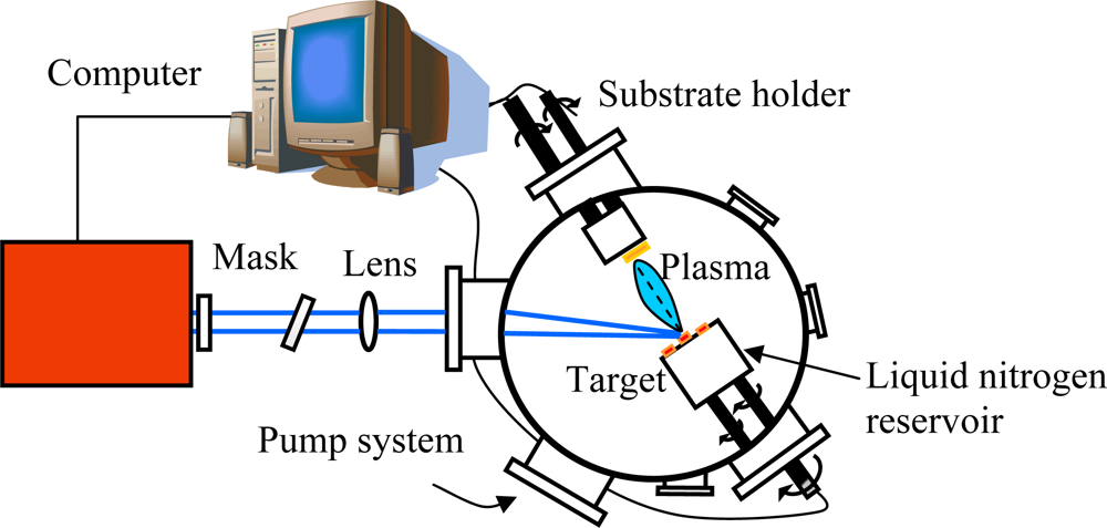
2. Experimental Apparatus and Procedure
3. Results and Discussion
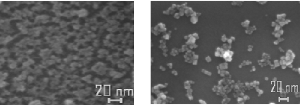
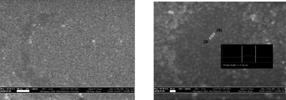
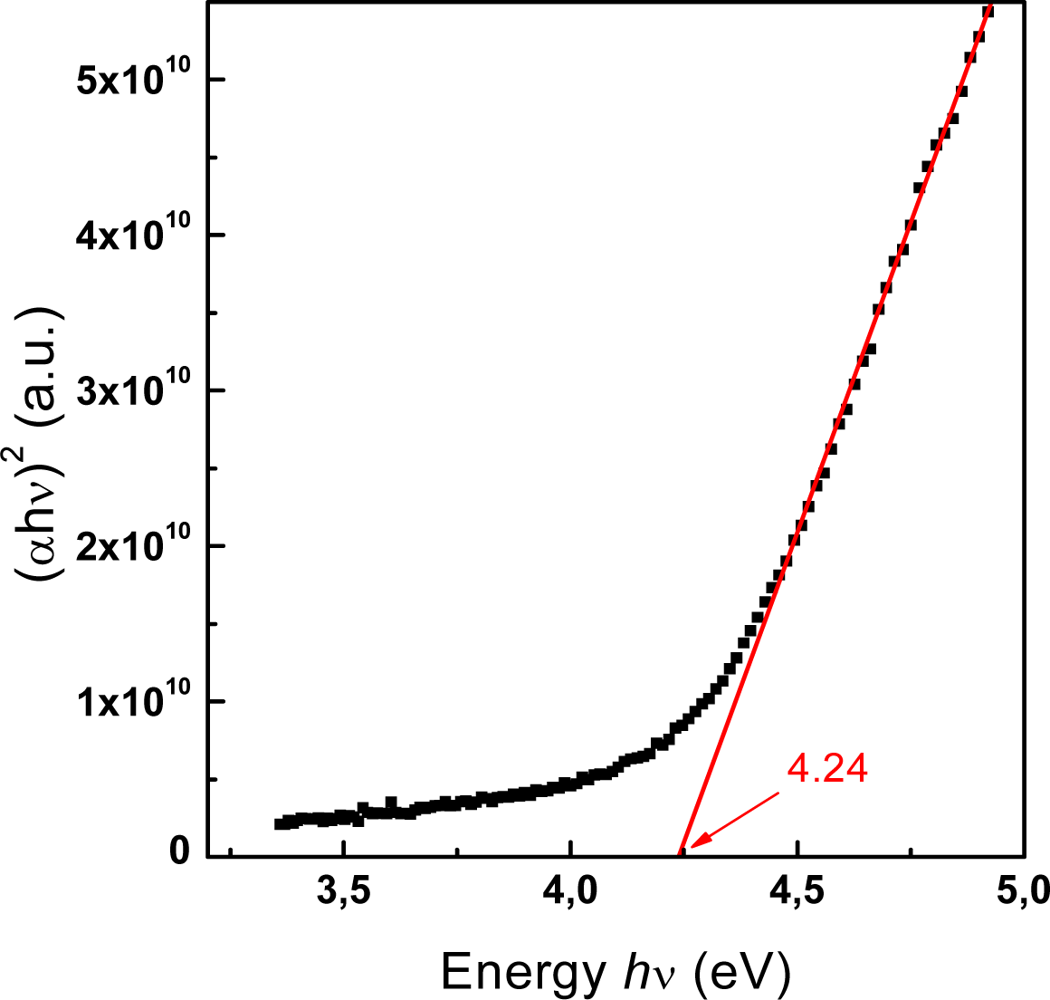
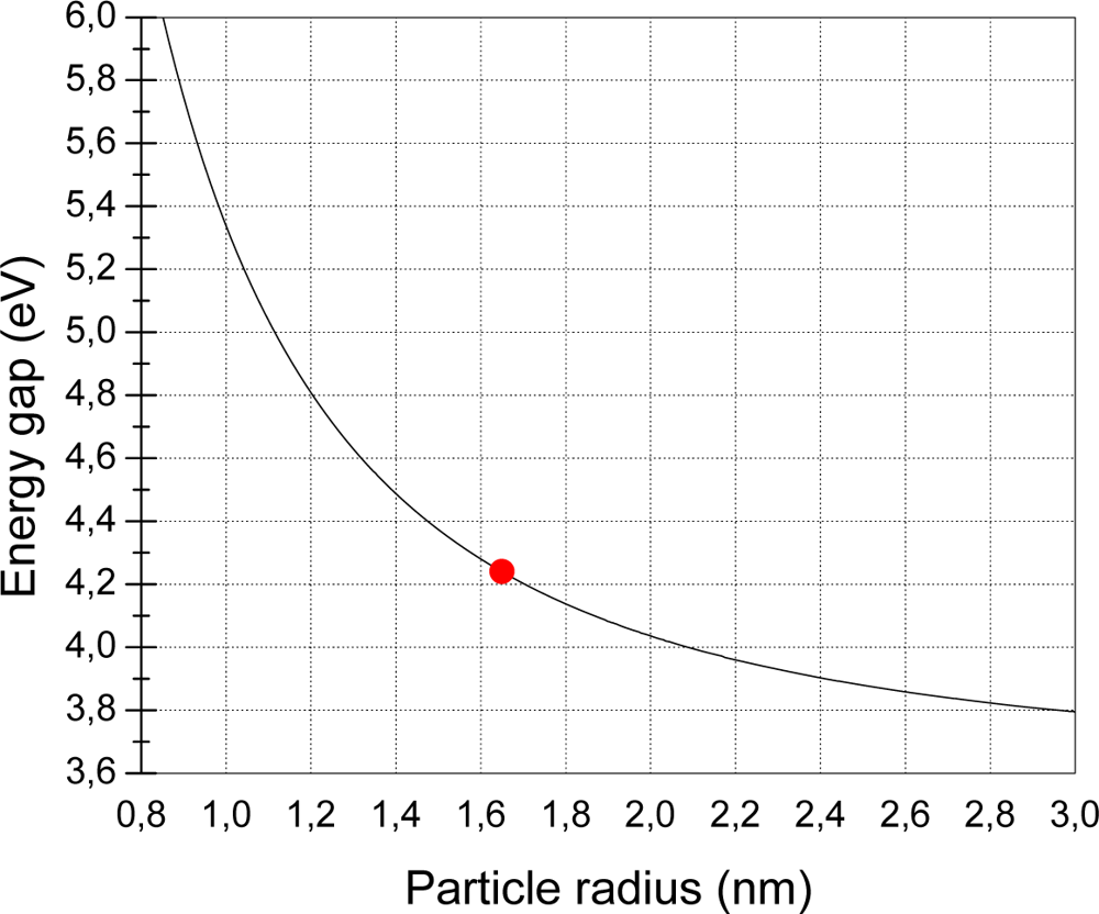
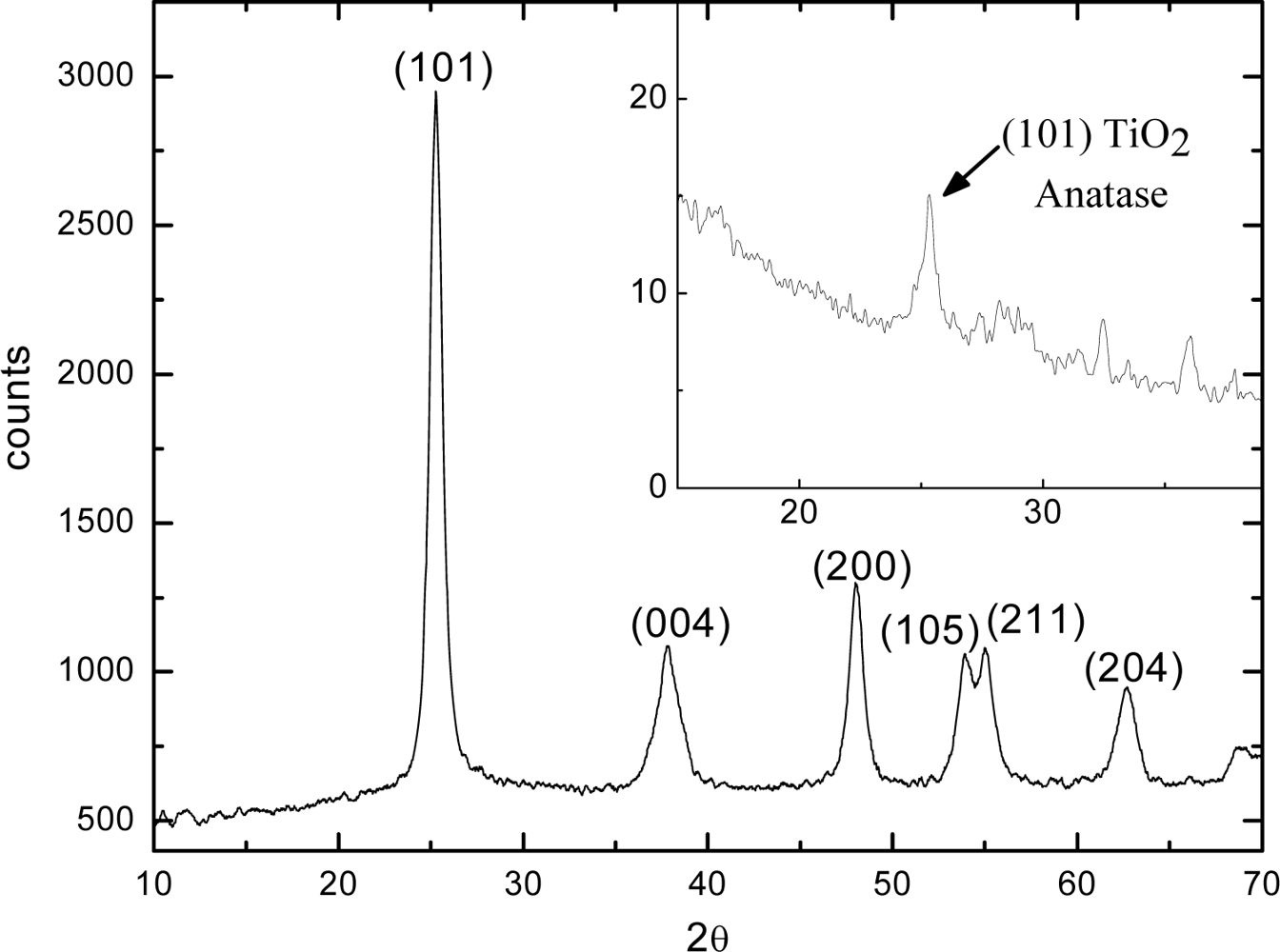
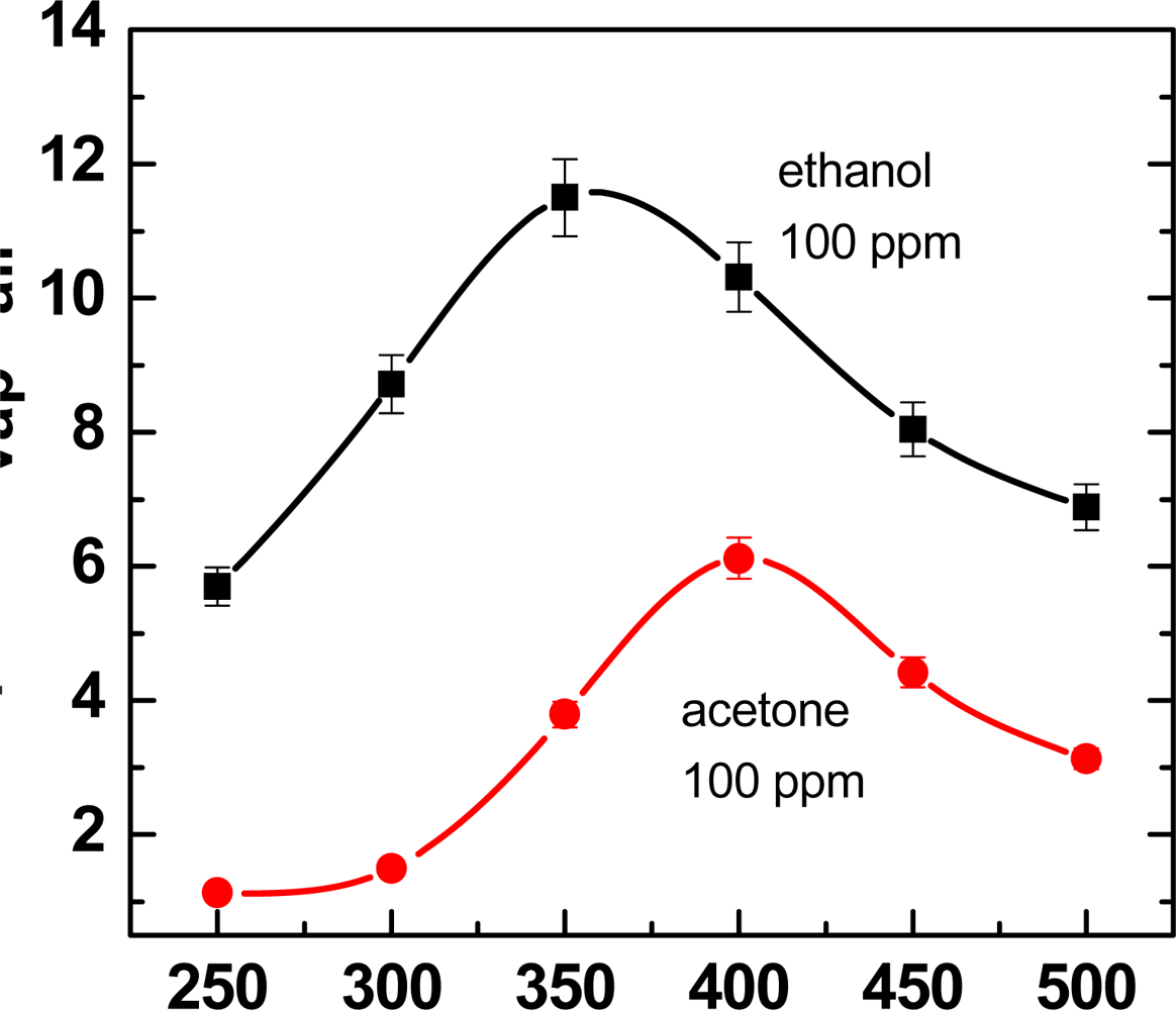
3.1. TiO2 nanoparticle films
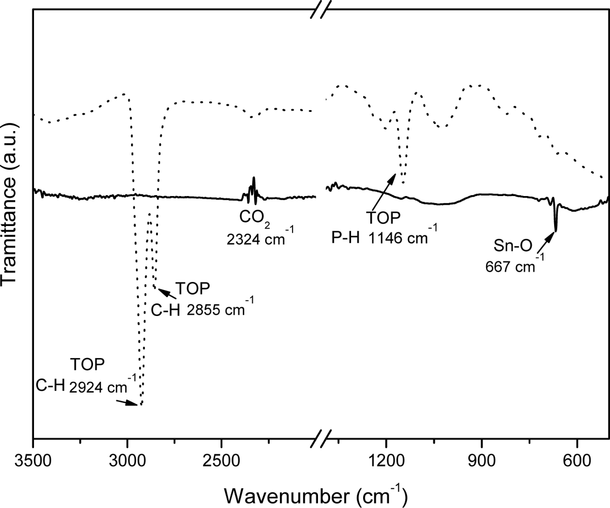
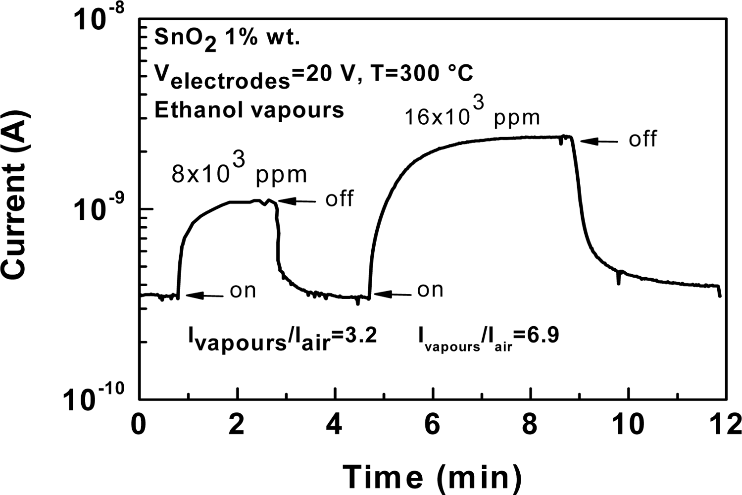
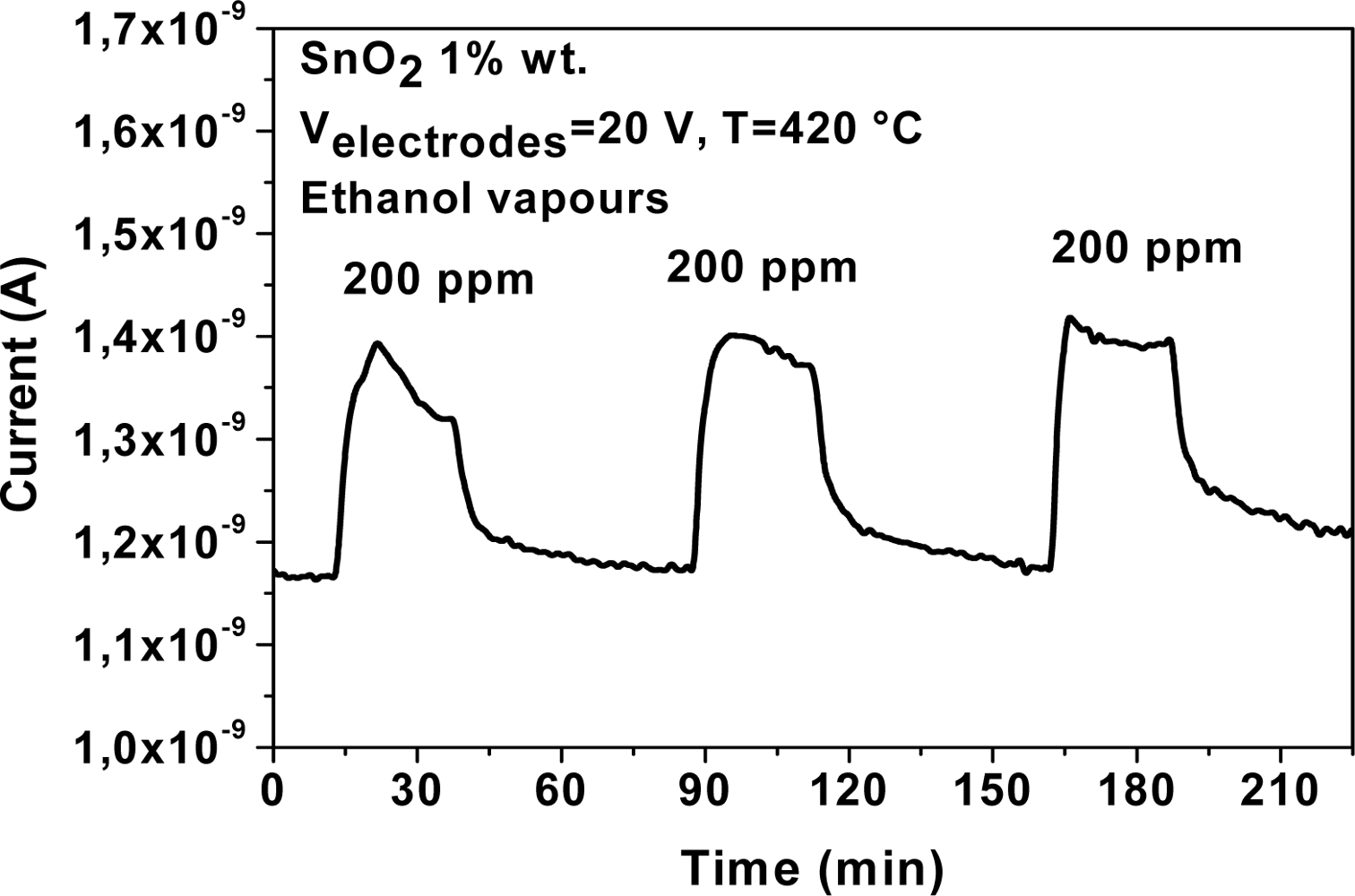
3.2. SnO2 nanoparticle films
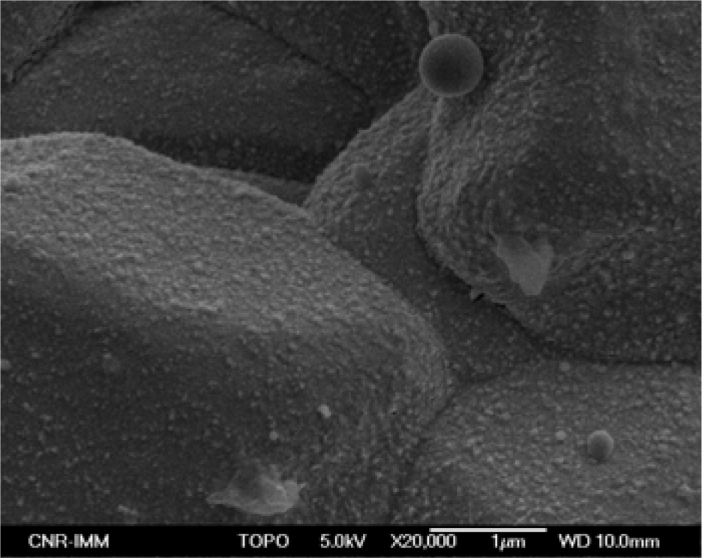
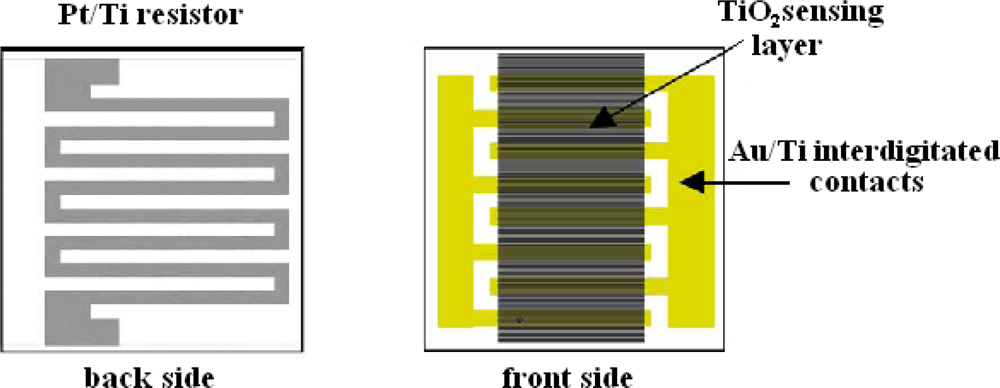
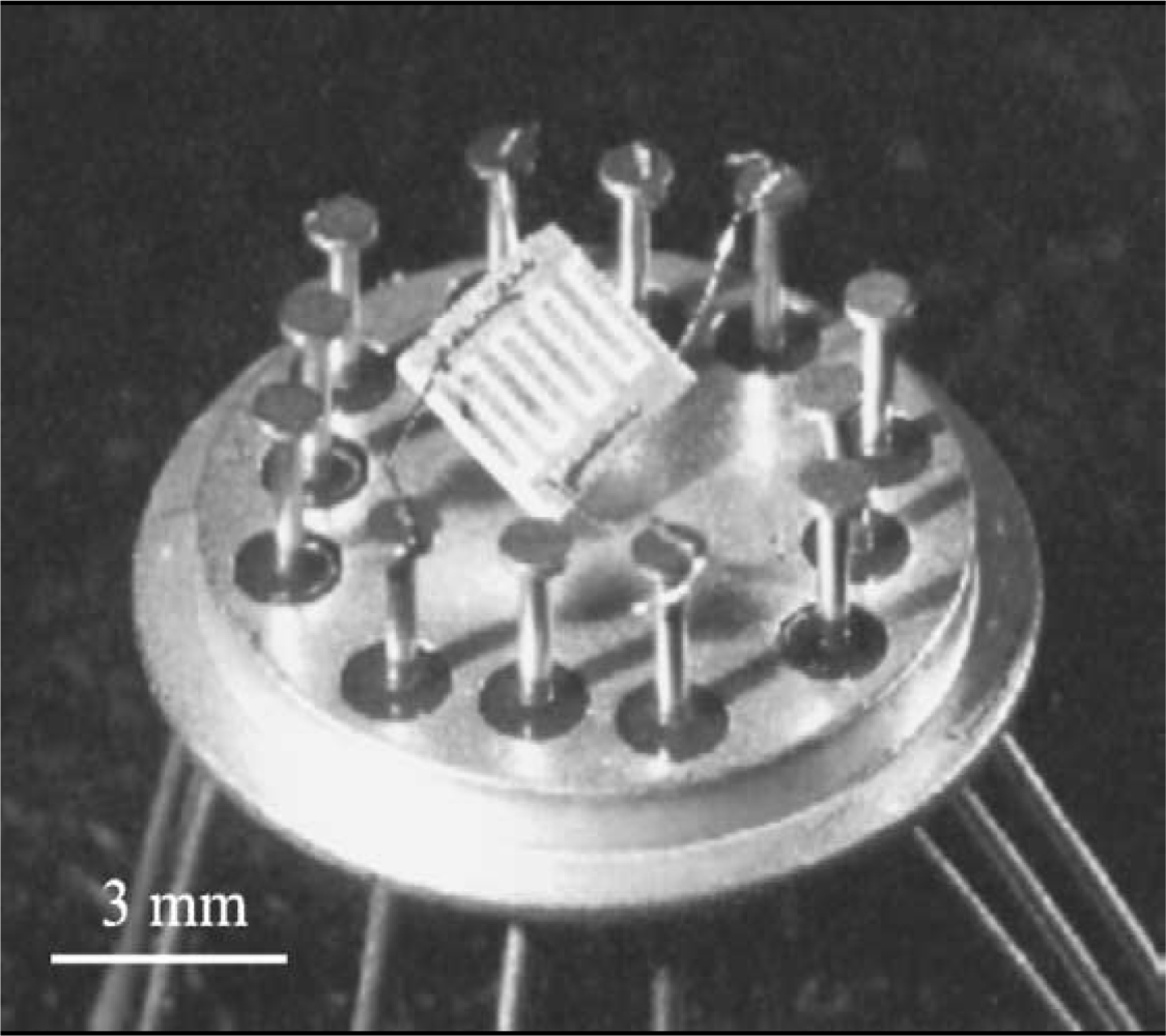
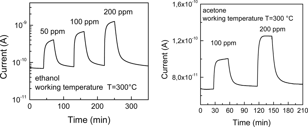
4. Sensor fabrication and characterization
5. Conclusions
Acknowledgments
References
- Kolasinski, K.W. Surface Science: Foundations of Catalysis and Nanoscience, 2nd Ed ed; JohnWiley&Sons Ltd: Chichester, U.K, 2008. [Google Scholar]
- Wu, Y.; Takeguchi, M.; Furuya, K. High Resolution Transmission Electron Microscopy Study on the Structure of Ge Nanoparticles by Using an Ultrahigh Vacuum-Molecular Beam Epitaxy-Transmission Electron Microscope System. Jpn. J. Appl. Phys 1999, 38, 7241–7246. [Google Scholar]
- Sun, Y.; Egawa, T.; Shao, C.; Zhang, L.; Yao, X. Formation Mechanism for High-Surface-Area Anatase Titania Nanoparticles Prepared by Metalorganic Chemical Vapor Deposition. Jpn. J. Appl. Phys 2004, 43, 3544–3547. [Google Scholar]
- Eason, R. Pulsed Laser Deposition of Thin Films; JohnWiley&Sons: Chichester, U.K., 2006. [Google Scholar]
- Lam, H.M.; Hong, M.H.; Yuan, S.; Chong, T.C. Growth of β-Ga2O3 Nanoparticles by Pulsed Laser Ablation Technique. Appl. Phys. A 2004, 79, 2099–2102. [Google Scholar]
- Teghil, R.; D'Alessio, L.; De Bonis, A.; Ferro, D.; Galasso, A.; Lanza, G.; Santagata, A.; Villani, P.; Sordelet, D.J. Ultra-short Pulse Laser Ablation of Al70Cu20Fe10 Alloy: Nanoparticles Generation and Thin Films Deposition. Thin Solid Films 2009, 517, 1880–1886. [Google Scholar]
- Epifani, M.; Arbiol, J.; Díaz, R.; Perálvarez, M.J.; Siciliano, P.; Rella, R. Synthesis of SnO2 and ZnO Colloidal Nanocrystals from the Decomposition of Tin(II) 2-Ethylhexanoate and Zinc(II) 2-Ethylhexanoate. Chem. Mater 2005, 17, 6468–6472. [Google Scholar]
- Kim, Y.J.; Kim, Y.S.; Chang, S.Y.; Cha, D.H.; Choi, Y.S.; Lee, W.I. Syntheses of Monodispersed SnO2 and CeO2 Nanoparticles through the Self-capping Role of 2-ethylhexanoate Ligands. New J. Chem 2007, 31, 260–264. [Google Scholar]
- Morandi, V.; Marabelli, F.; Amendola, V.; Meneghetti, M.; Comoretto, D. Colloidal Photonic Crystals Doped with Gold Nanoparticles: Spectroscopy and Optical Switching Properties. Adv. Funct. Mater 2007, 17, 2779–2786. [Google Scholar]
- Kontturi, E.; Johansson, L.S.; Kontturi, K.S.; Ahonen, P.; Thüne, P.C.; Laine, J. Cellulose Nanocrystal Submonolayers by Spin Coating. Langmuir 2007, 23, 9674–9680. [Google Scholar]
- Sigman, M.B.; Saunders, A.E.; Korgel, B.A. Metal Nanocrystal Superlattice Nucleation and Growth. Langmuir 2004, 20, 978–983. [Google Scholar]
- Caricato, A.P.; Manera, M.G.; Martino, M.; Rella, R.; Romano, F.; Spadavecchia, J.; Tunno, T.; Valerini, D. Uniform Thin Films of TiO2 Nanoparticles Deposited by Matrix Assisted Pulsed Laser Evaporation. Appl. Surf. Sci 2007, 253, 6471–6475. [Google Scholar]
- Caricato, A.P.; Epifani, M.; Martino, M.; Romano, F.; Rella, R.; Taurino, A.; Tunno, T.; Valerini, D. MAPLE Deposition and Characterization of SnO2 Colloidal Nanoparticle Thin Films. J. Phys. D: Appl. Phys 2009, (in press).. [Google Scholar]
- Madhushudana Reddy, M.H.; Chandorkar, A.N. Response Study of Electron-beam Evaporated Thin-film Tin Oxide Gas Sensors. Sens. Actuat. B 1992, 9, 1–8. [Google Scholar]
- Vlachos, D.S.; Xenoulis, A.C. Gas detection sensitivity and cluster size. Nanostruct. Mater 1998, 10, 1355–1361. [Google Scholar]
- Rella, R.; Spadavecchia, J.; Manera, M.G.; Capone, S.; Taurino, A.; Martino, M.; Caricato, A.P.; Tunno, T. Acetone and ethanol solid-state gas sensors based on TiO2 nanoparticles thin film deposited by matrix assisted pulsed laser evaporation. Sens. Actuat. B 2007, 127, 426–431. [Google Scholar]
- Caricato, A.P.; Capone, S.; Ciccarella, G.; Martino, M.; Rella, R.; Romano, F.; Spadavecchia, J.; Taurino, A.; Tunno, T.; Valerini, D. TiO2 nanoparticle thin film deposition by matrix assisted pulsed laser evaporation for sensing applications. Appl. Surf. Sci 2007, 253, 7937–7941. [Google Scholar]
- Pinna, N.; Neri, G.; Antonietti, M.; Niederberger, M. Nonaqueous Synthesis of Nanocrystalline Semi-Conducting Metal Oxides for Gas Sensing. Angew. Chem. Int. Ed 2004, 43, 4345–4349. [Google Scholar]
- Burns, G. Solid State Physics; Academic Press: New York, U.S.A., 1985. [Google Scholar]
- Serpone, N.; Lawless, D.; Khairutdinov, R. Size Effects on the Photophysical Properties of Colloidal Anatase TiO2 Particles: Size Quantization versus Direct Transitions in This Indirect Semiconductor? J. Phys. Chem 1995, 99, 16646–16654. [Google Scholar]
- Coutinho, J.P.G.; Barbosa, M.T.C.M. Characterization of TiO2 Nanoparticles in Langmuir-Blodgett Films. J. Fluoresc 2006, 16, 387–392. [Google Scholar]
- Rowsell, B.D.; Veinot, J.G.C. Reductive thermolysis of a heterocyclic precursor: a convenient method for preparing luminescent, surfactant-stabilized silicon nanoparticles. Nanotechnology 2005, 16, 732–736. [Google Scholar]
- Gu, F.; Wang, S.F.; Song, C.F.; Lu, M.K.; Qi, Y.X.; Zhou, G.J.; Xu, D.; Yuan, D.R. Synthesis and luminescence properties of SnO2 nanoparticles. Chem. Phys. Lett 2003, 372, 451–454. [Google Scholar]
- Suda, Y.; Kawasaki, H.; Namba, J.; Iwatsuji, K.; Doi, K.; Wada, K. Properties of palladium doped tin oxide thin films for gas sensors grown by PLD method combined with sputtering process. Surf. Coat. Technol 2003, 174–175, 1293–1296. [Google Scholar]
- Lee, E.J.H.; Ribeiro, C.; Giraldi, T.R.; Longo, E.; Leite, E.R.; Varela, J.A. Photoluminescence in Quantum-confined SnO2 Nanocrystals: Evidence of Free Exciton Decay. Appl. Physics Letters 2004, 84, 1745–1747. [Google Scholar]
- Das, S.; Kar, S.; Chaudhuri, S. Optical Properties of SnO2 Nanoparticles and Nanorods Synthesized by Solvothermal Process. J. Appl. Phys 2006, 99, 114303 (1–7). [Google Scholar]
- Brus, L.E. Electron–electron and Electron-hole Interactions in Small Semiconductor Crystallites: The Size Dependence of the Lowest Excited Electronic State. J. Chem. Phys 1984, 80, 4403–4409. [Google Scholar]
- Izydorcyzk, W.; Adamowicz, B.; Miczek, M.; Waczynski, K. Computer analysis of an influence of oxygen vacancies on the electronic properties of the SnO2 surface and near-surface region. Phys. Status Solidi (a) 2006, 203, 2241–2246. [Google Scholar]
- Zhang, G.; Liu, M. Effect of particle size and dopant on properties of SnO2-based gas sensors. Sens. Actuat. B 2000, 69, 144–152. [Google Scholar]


© 2009 by the authors; licensee MDPI, Basel, Switzerland This article is an open access article distributed under the terms and conditions of the Creative Commons Attribution license (http://creativecommons.org/licenses/by/3.0/).
Share and Cite
Caricato, A.P.; Luches, A.; Rella, R. Nanoparticle Thin Films for Gas Sensors Prepared by Matrix Assisted Pulsed Laser Evaporation. Sensors 2009, 9, 2682-2696. https://doi.org/10.3390/s90402682
Caricato AP, Luches A, Rella R. Nanoparticle Thin Films for Gas Sensors Prepared by Matrix Assisted Pulsed Laser Evaporation. Sensors. 2009; 9(4):2682-2696. https://doi.org/10.3390/s90402682
Chicago/Turabian StyleCaricato, Anna Paola, Armando Luches, and Roberto Rella. 2009. "Nanoparticle Thin Films for Gas Sensors Prepared by Matrix Assisted Pulsed Laser Evaporation" Sensors 9, no. 4: 2682-2696. https://doi.org/10.3390/s90402682