1. Introduction
Surface Acoustic Wave (SAW) devices are considered to be one of the early examples of Micro-Electromechanical systems (MEMS) [
1] due to the coupling needed between electrical and mechanical properties during wave propagation on the surface of these devices. These devices' high reliability and relative simplicity in fabrication and integration motivated MEMS researchers to utilize it in a broad range of applications such as TVs, VCRs, radar systems, wireless headsets, alarm systems and mobile phones. In addition, the propagation of the wave along the surface allows it to be sensitive to changes in the external environment; therefore SAW sensors have been developed for numerous applications such as gas detection [
2], fluid viscosity changes [
3], and pressure changes [
4], determination of stiffness constants [
5] and detection of the onset of ice formation on aerospace structures [
6].
The design process for SAW devices is highly iterative due to the various parameters that could be manipulated to utilize its sensitivity; such as electrode dimensions, size, shape and configuration, piezoelectric substrate material, waveguide material and dimensions, operating frequency and mode of wave propagation. In addition, there is a wide range of complex electromechanical interactions that take place in a typical SAW device. To optimize the design phase various numerical and analytical techniques have been developed and some are used concurrently.
The Delta function model is one of the earliest and basic modeling techniques of SAW devices. This model provides a basic understanding of the response of SAW devices. It only provides relative insertion loss since it does not take into consideration impedance level and second order effects [
7]. However, this model provides very good information on bandwidth, rejection levels and side lobes. When a voltage signal is applied to the inter-digital (IDT) electrodes, there is an instantaneous charge accumulation. Due to the alternating polarity of adjacent electrodes the charges accumulate towards the edges of an electrode. This model represents the charge distribution on the surface of the electrodes as discrete delta functions. The magnitude of the delta functions is proportional to the amplitude of the applied voltage signal. The total response of an IDT due to an applied voltage signal is obtained by summing the delta functions on the electrodes.
The Coupling of Modes (COM) approach is another technique used to model SAW devices. This technique branches out of the general wave propagation field in periodic structures, which covers a wide range of wave phenomena such as electromagnetic waves in periodic gratings, optical and ultrasonic waves in multi-layered media, phonon propagation and X-ray scattering in crystals, quantum theory of electron states in metals, semiconductors and dielectrics [
8]. The coupling of modes approximation indicates that in periodic structures only the incident wave and the reflected wave with strong coupling are considered [
8]. The two waves are counter-propagating and a linear coupling is assumed between the amplitudes, voltage and current. The spatial variation of the amplitude of the two modes and the current generated in the conducting electrodes are described through a set of first order linear differential equations. The COM equations are often represented, for convenience by the P-matrix method developed by Tobolka [
9]. The P-matrix represents an IDT structure as a three port network with two acoustical ports and a third electrical port. The coefficients of the P-Matrix are determined from the COM parameters; velocity, reflectivity, transduction coefficient, attenuation and capacitance.
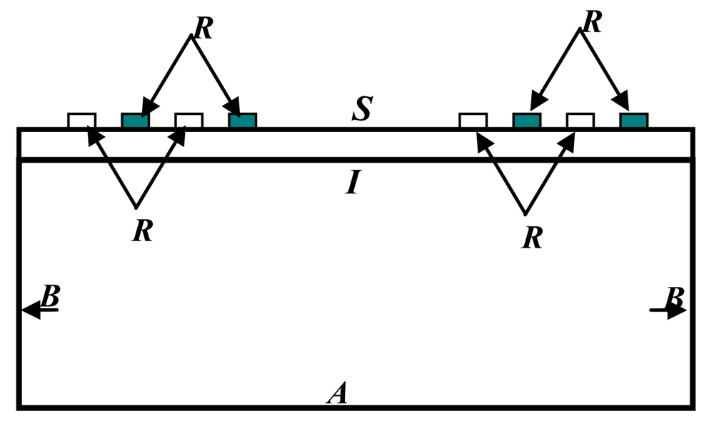
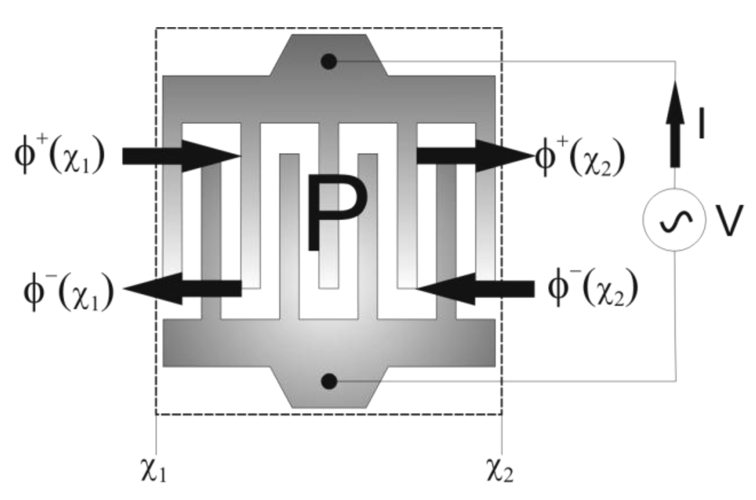
Figure 1 illustrates an IDT structure as a three port network. The boundary conditions are the applied voltage
V and the incident waves with amplitudes
φ+(
x1) and
φ−(
x2), respectively. The response of the device is represented by the current (
I) generated at the electrodes and the reflected waves with amplitudes
φ−(
x1) and
φ+(
x2).
The P-matrix representation of an IDT structure relating the boundary conditions to device response is given by:
The upper left sub-matrix describes the scattering of the incident waves. The coefficients P11 = P22 are reflection coefficients and P12 = P21 are transmission coefficients. The remaining elements of the P-matrix represent the electrical properties of the device; P13 and P23 describe the electro-acoustic transfer function of the IDT. The components P31 and P32 determine the current generated in the IDT by the arriving waves. The P33 term is the admittance term, which relates the generated current to the applied voltage. One of the main advantages of the P-matrix method is its simplicity in modeling devices with different sub-structures. A separate P-matrix can be developed for each sub-structure of the SAW device and all can be cascaded into one P-matrix that represents the whole device.
The Equivalent Circuit model is another modeling technique, whose representation is close to the P-matrix. In this modeling technique, the equivalent circuit of the SAW device is developed and the IDT structure is modeled as a three port network [
7]. Two ports are the electrical equivalent of the two acoustic ports in the P-matrix and the third port is an actual electrical port at which the input and output signals are applied and detected. The boundary conditions in this case are the applied voltages, while the response is considered to be current generation at the three ports. The boundary conditions are related to the response through the admittance matrix. The electrical parameters of the equivalent circuit are determined from wave and device properties such as wave velocity, substrate electromechanical coupling coefficient, centre frequency and number of electrode pairs. As in the P-matrix approach, an IDT with different sub-structures can be easily modeled by cascading the various admittance matrices for the sub-structures and then obtaining the overall transfer function of the SAW device from the ratio of output to input voltage.
The FE method can be used concurrently with the COM and equivalent circuit models. The COM parameters pertaining to the device configuration need to be determined to be used as input for these models. Test structures could be fabricated and analyzed in order to extract the necessary parameters. However, the experimental approach is both expensive and time consuming since the necessary parameters have to be extracted for each device configuration. On the other hand, the FE method provides an alternative approach for determining the device parameters in a time and cost efficient manner. The ability to model SAW devices is based on the well established theory of applying the FE method to piezoelectric vibration. The finite element formulation of piezoelectric media is provided at a later section in this article, however, a comprehensive review is also available in [
10,
11]. This numerical technique provides a greater flexibility in modeling SAW devices because it can handle the wave equations in two and three dimensions. This allows capturing the full device response and enhances the ability to model complex geometries and test different designs for optimum performance.
Various researchers have successfully modeled SAW sensors using the FE method to investigate different aspects of these devices such as sensor response to mass loading [
12-
14], various device configurations [
15,
16], power consumption evaluation [
1] and mass sensitivity evaluation [
17]. A common problem in modeling SAW devices is the increased computational capacity, which often arises due to the mandatory requirement of having a sufficient number of elements along the wavelength in the propagation path. This requirement ensures that the wave is fully captured and hence the sensor response is accurate. The operating frequency and wave velocity in SAW devices are relatively high, where the wavelengths are usually in the micrometer range, therefore the size of the elements have to be significantly reduced with respect to the wavelength to accurately capture the response. This leads to an increase in the overall number of elements in the FE model and hence increases the computational capacity. Various researchers have reported constraints due to the increased computational requirements of the FE models and made various attempts to reduce it [
15,
17-
20]. Some of these attempts include reducing sensor dimensions, developing a two dimensional model and manipulating element sizes to reduce overall element count.
In almost all of the FE models referred to above, bulk piezoelectric substrates are adopted, such as lithium niobate (LiNbO
3), quartz, langasite (LGS) and lithium tantalate (LiTaO
3). The most common orientation of these substrates are Y-Z LiNbO
3, ST-X Quartz, Z-X LiNbO
3 and 36 Y-X LiTaO
3 with the corresponding SAW velocities of 3,488 m/s [
15], 3,159 m/s [
21], 3,797 m/s [
22] and 4,220 m/s [
23], respectively. The limitation due to model size poses a greater obstacle to modeling new trends in SAW devices. Current development is heading towards producing a fully integrated system on one chip referred to as a Monolithic Chip [
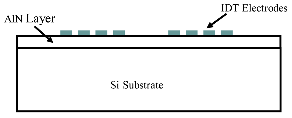
24]. The chip allows the integration of all system components in a single platform, reduction in size, low fabrication cost, mass production and low power consumption. Bulk piezoelectric materials are incompatible with planar integrated circuit technology; therefore, “layered” SAW devices are being developed. A layered SAW device consists of a silicon substrate covered by thin piezoelectric film. This configuration requires materials that can be deposited with high piezoelectric properties that closely match the corresponding single crystal properties. The two most widely used materials are Aluminum Nitride (AlN) and Zinc Oxide (ZnO) [
25] since both materials possess exceptionally high piezoelectric properties. In addition, both can be deposited in a well oriented structure on a variety of substrates such as silicon, sapphire, diamond, graphite and glass. However, AlN is more widely adopted due to its higher resistivity and higher SAW velocity; 5,067 m/s [
26]. This allows achieving much higher frequency levels than that attainable with bulk piezoelectric materials hence leading to even smaller wavelengths.
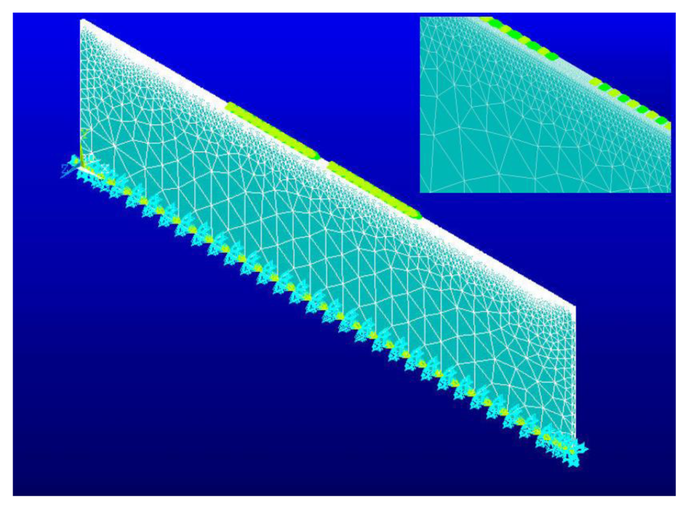
In this study, the FE method is used to develop an idealized model of a layered SAW sensor, with AlN used as the piezoelectric film on a silicon substrate. The idealized model is a “Reduced” 3D (R3D) model. The model assumes a plane wave solution, therefore, the wave properties vary in two dimensions only and is uniform in the third dimension; the thickness direction. This idealization allows minimizing the thickness of the sensor, which reduces the overall required number of elements. The results of the R3D model are compared to experimental and theoretical frequency data. In addition, the frequency response and insertion loss values of the R3D model are compared to those of 2D models with similar configuration.
3. Numerical Model of the SAW Sensor Using the Finite Element Method
The equations of piezoelectricity are fairly complex to allow a closed form solution and therefore, FE analysis is commonly used to provide an approximate solution to these equations using the variational and the virtual work principles. The virtual work per unit area created by surface tractions (
f) due to a small virtual displacement (
u) of the surface is {
δu}
t {
f}. The electrical analog of the work due to the surface tractions (
f) is the work created by the charge density (
q) due to a virtual electric potential
φ. The work due to charge density is expressed as −
q{
δφ}. The total virtual work done on the surface of the body is:
The variational principle is expressed as:
The Lagrangian operator in this case consists of the difference between the kinetic energy and the electrical enthalpy L = E
Kin – H rather than the difference between the kinetic energy and the internal energy as in the case of pure elasticity [
10]. The electrical enthalpy
H is defined as the difference between the elastic energy (E
ST) and the summation of the electro-mechanical (E
EM) and dielectric energy (E
D), H = E
ST – [E
EM + E
D] [
28].
The kinetic Energy is defined as:
and the elastic energy E
ST is defined as:
The Electro-mechanical coupling energy E
EM is defined as:
The dielectric energy E
D is defined as:
Expressing the work
W in terms of body, surface and point loads and charges leads to:
where:
fb: mechanical body force vector (N/m3)
fs: mechanical surface force vector (N/m2)
fp: mechanical point forces (N)
qs: surface charges (C/m2)
qp: point charges (C)
In the FE formulation the body is discretized into finite elements, where the mechanical displacements
u, electrical potential
φ, electrical charge
q and mechanical forces
f are calculated at the nodes of these elements. The value at any position in the element is determined by means of linear combinations of polynomial interpolation functions
N and the nodal values of these quantities as coefficients:
Similarly, for the electric potential
φ and electric charge
q:
These expressions are then substituted in
Equation (18) then into
Equation (13). The Strain
S and the electric field
E, which are obtained by differentiating the displacement and the electric potential respectively can be expressed as:
| Mass Matrix [M] | |
| Mechanical Stiffness Matrix [Kuu] | |
| Mechanical Body Force Matrix [FB] | |
| Mechanical Surface Force Matrix [FS] | |
| Mechanical Point Force Matrix [FP] | |
| Mechanical Damping Matrix [Duu] | |
| Piezoelectric Coupling Matrix [Kuφ] | |
| Dielectric Stiffness Matrix [Kφφ] | |
| Electrical Surface Charge Matrix [Qs] | |
| Electrical Point Charge Matrix [QP] | |
| *α and β are Damping coefficients |
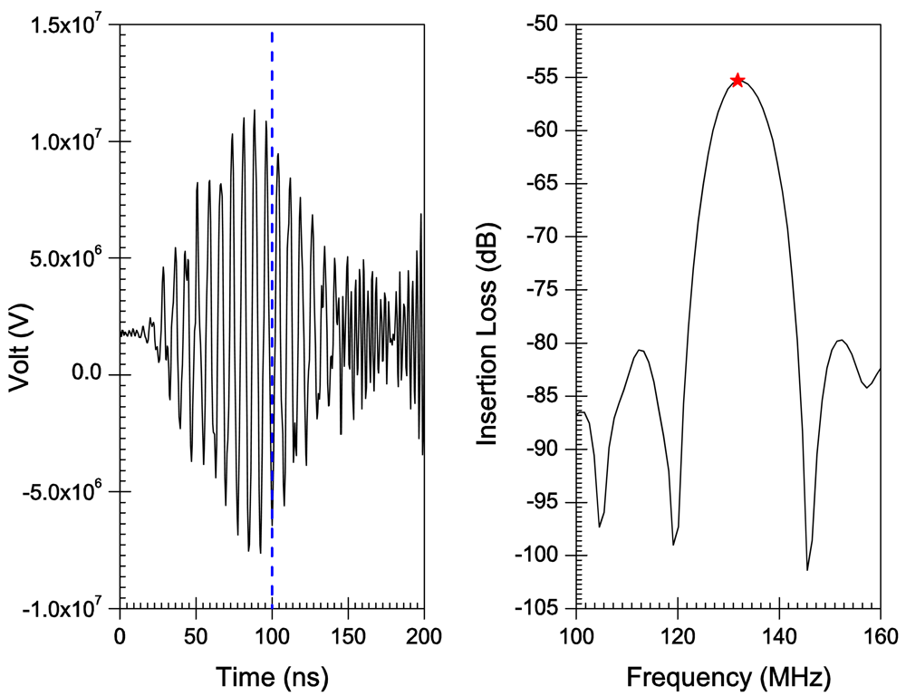
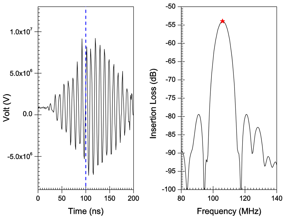
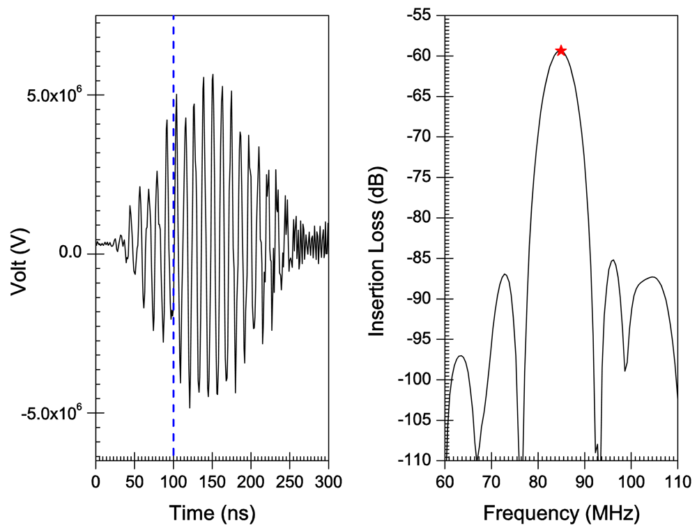
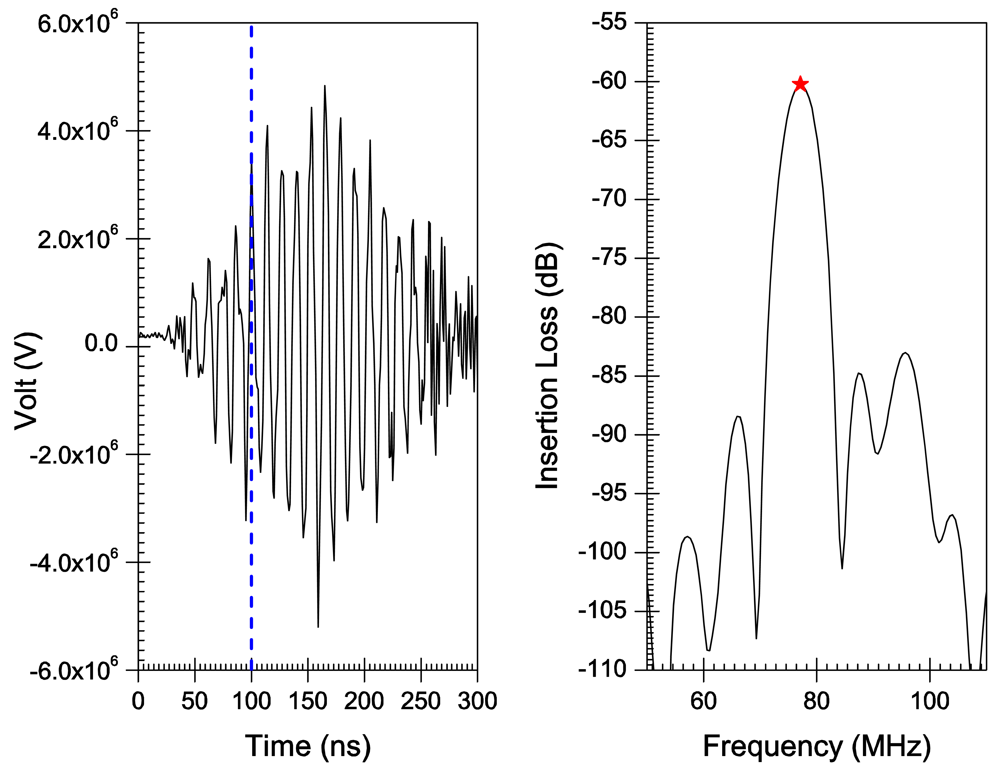
6. Discussion
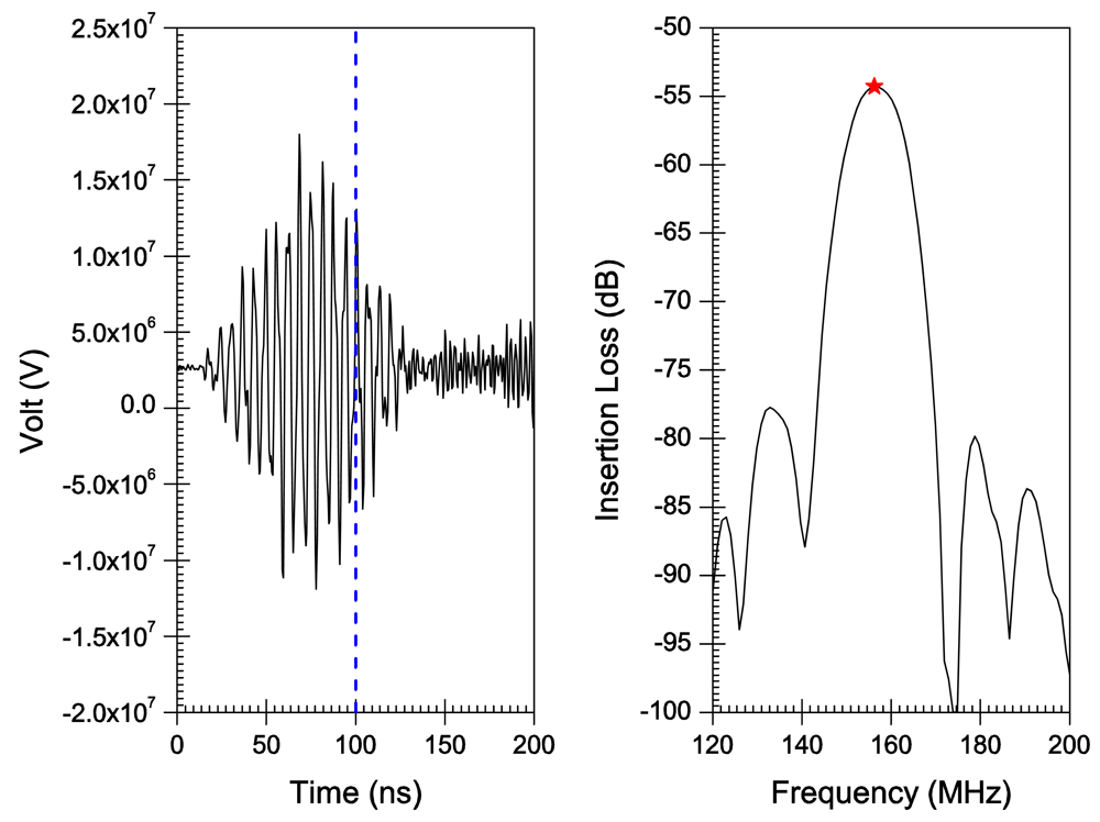
A transient analysis is carried out using FEA to obtain the time-domain response of AlN/Si(111) SAW sensors adopting different
h/λ values. The frequency response is then obtained by Fourier transform of the transient response for each configuration. Response curves in time and frequency domains are illustrated in
Figures 6–
10 for
h/λ values from 0.1 to 0.2. Hypothetical lines (---) are inserted in the transient response curves at 100 ns to illustrate the delay in wave speed that takes place due to decreasing
h/λ values. For
h/λ values of 0.2 and 0.17 the transient response reaches its peak prior to 100 ns, however as
h/λ decreases the peak of the transient response shifts further away from 100 ns indicating a delay in the wave speed.
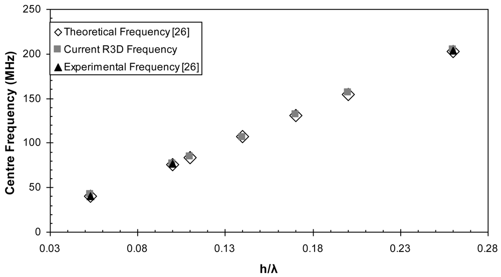
This behavior illustrates the dispersion property of the SAW wave, where the velocity of the wave changes accordingly with the thickness of the AlN film. As the SAW propagates along the surface of the layered AlN/Si(111) structure its velocity varies between that of AlN and silicon. The SAW velocity in AlN is higher than that in silicon; 5,607 and 4,550 m/s, respectively [
31]. The increase in the
h/λ parameter causes the wave to become more confined in the AlN layer, therefore its velocity increases until it eventually reaches that of AlN. The increase in wave velocity leads to an increase in the centre frequency of the SAW device as illustrated by
Equation (30), which predicts a linear behavior. The centre frequency values for the different
h/λ configurations are plotted in
Figure 11 and a linear behavior is obtained as expected.
By adopting the plane wave solution
Equation (8) the thickness of the sensor could be kept to a minimum while allowing polarizations in all three directions. Comparing the frequency response of the R3D model with the theoretical and experimental data shows very good agreement as illustrated in
Figure 11. The reduced size of the model gives a higher flexibility in reducing the element size sufficiently along the propagation path and hence increasing the number of elements per wavelength to accurately capture the response.
The widely adopted approach in the literature is to develop 2D models in order to reduce the number of elements of the FE model significantly and reduce the required computational capacity. The main drawback in the 2D approach is that the displacement in the shear-horizontal direction is decoupled, which reduces the accuracy of the results. In order to demonstrate the impact of the R3D model, several 2D FE models of SAW devices with AlN/Si(111) layout were developed with similar h/λ values to the R3D models.
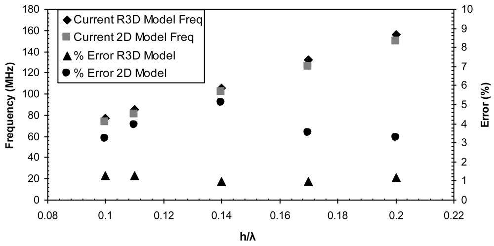
Figure 12 illustrates the frequency response of the R3D model in comparison with the 2D model for the different
h/λ values. The error (%) with respect to the theoretical frequency values [
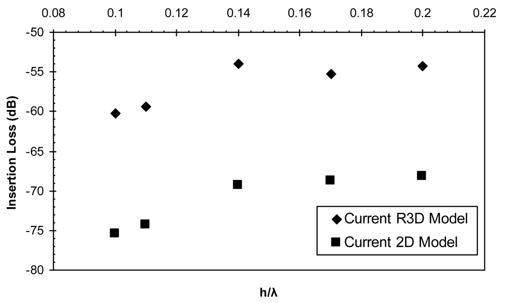
26] is also plotted to illustrate the accuracy of both modeling approaches. The error (%) for the center frequency values of the R3D model are within 1%, however for the 2D model the error (%) varies between 3-5%. In addition, the insertion loss values of the R3D model and the 2D model are plotted in
Figure 13. Results show a major discrepancy for all the
h/λ values. The significant variations of the 2D model are due to the decoupling of the displacement component in the shear-horizontal direction.


