Article

Experimental-Numerical Comparison of the Cantilever MEMS Frequency Shift in presence of a Residual Stress Gradient

1
Department of Mechanics, Politecnico of Torino, C.so Duca degli Abruzzi,24 - 10129, Torino, Italy
2
Faculty of Mechanical Engineering, State University of Campinas, CEP 13083-970 Campinas, Brazil
*
Author to whom correspondence should be addressed.
Sensors 2008, 8(2), 767-783; https://doi.org/10.3390/s8020767
Submission received: 19 November 2007 / Accepted: 28 January 2008 / Published: 6 February 2008
(This article belongs to the Special Issue Modeling, Testing and Reliability Issues in MEMS Engineering)

Abstract

:
The dynamic characterization of a set of gold micro beams by electrostatic excitation in presence of residual stress gradient has been studied experimentally. A method to determine the micro-cantilever residual stress gradient by measuring the deflection and curvature and then identifying the residual stress model by means of frequency shift behaviour is presented. A comparison with different numerical FEM models and experimental results has been carried out, introducing in the model the residual stress of the structures, responsible for an initial upward curvature. Dynamic spectrum data are measured via optical interferometry and experimental frequency shift curves are obtained by increasing the dc voltage applied to the specimens. A good correspondence is pointed out between measures and numerical models so that the residual stress effect can be evaluated for different configurations.

1. Introduction

Micro-electromechanical systems (RF-MEMS) have recently demonstrated advances in the field of radio-frequency in the realization of tuneable circuits including phase shifters, filters and matching networks. Although great improvements have been made in the reliability of these devices, significant gaps remain in the understanding of fundamental mechanical properties such as stress/strain relationships and the origin of residual stress within the thin-film metals used for the mechanical structure [1,2]. Residual stress/strain becomes a parameter of fundamental importance in micro-structure, surface micromachining and improving reliability of micro-devices [3-5].
There has been a lot of research into controlling residual stress by controlling fabrication process parameters, for example by adjusting the bath compositions or selecting the seed layer material used for the growing of the suspended parts [6,7]. Also, the vapour deposition was indicated as cause of either high compressive or tensile residual stress gradients, depending on the deposition process.
Residual stress causes the change of equilibrium configuration and variation of important system parameters such as resonant frequencies and pull-in tension. In recent literature residual stress in microbeams has been studied, being considered as unavoidable in surface micromachining techniques: in [8] 1D and 2D models are presented considering residual stress, fringing-field effect and axial stress due to great deflections. The contribution of each of these three effects on pull-in voltage is analyzed using dimensionless numbers. In [9] the residual stress of etched thin films was computed as a function of the deflection amplitude, by calculating the total potential energy stored in a slightly curved beam. In [4] residual stress also was estimated by studying the static deformation of microfabricated bridges, while in [10] stress measurement was obtained at first with wafer curvature measurement before and after deposition, then with silicon structures designed on this porpoise. In [11] stress gradient was calculated from cantilever curvature; deflection variations were observed by changing process parameters such as plasma ashing time.
In coupled electromechanical systems the natural frequency values decrease as the voltage increases. This characteristic makes it possible, for example, to tune an operating frequency with an applied bias voltage [12]. Forecasting this voltage dependent frequency behaviour becomes thus an important issue. The identification of the frequency shift curve can be experimentally related to the presence of residual stress. Dynamic theoretical behaviour of microstructures was already investigated by the authors in [13-15], analytical and numerical solutions were described and compared and an assessment of the available approaches to simplify the continuous nonlinear model was proposed. Among the presented models there was the Newmark direct integration method modified to consider the electromechanical coupled-field effects of MEMS, an eigensensitivity approach using the modal solution of an eigenvalue problem and reduced order models within ANSYS™.
In the present work a set of experimental tests was conducted to evaluate the frequency shift of curled cantilever gold beams. Typical RF-MEMS devices consist of either clamped beams or cantilevers. Due to its low electrical loss and chemical inertness, gold is the most common material for fabricating these structures. Despite these benefits, the high susceptibility to relaxation effects of gold often introduce much residual stress into these RF-MEMS structures [16].
The deflection profile of microcantilevers was obtained through a non-contact interferometric profilometry system using the fringe pattern generated by interference. Once the deflection profile is measured, the slope and curvature can be easily calculated. The models presented in this paper can thus uniquely determine the resultant bending moment due to residual stress gradients, furthermore it is possible to identify the dynamic behaviour of the specimen from zero dc voltage to pull-in.

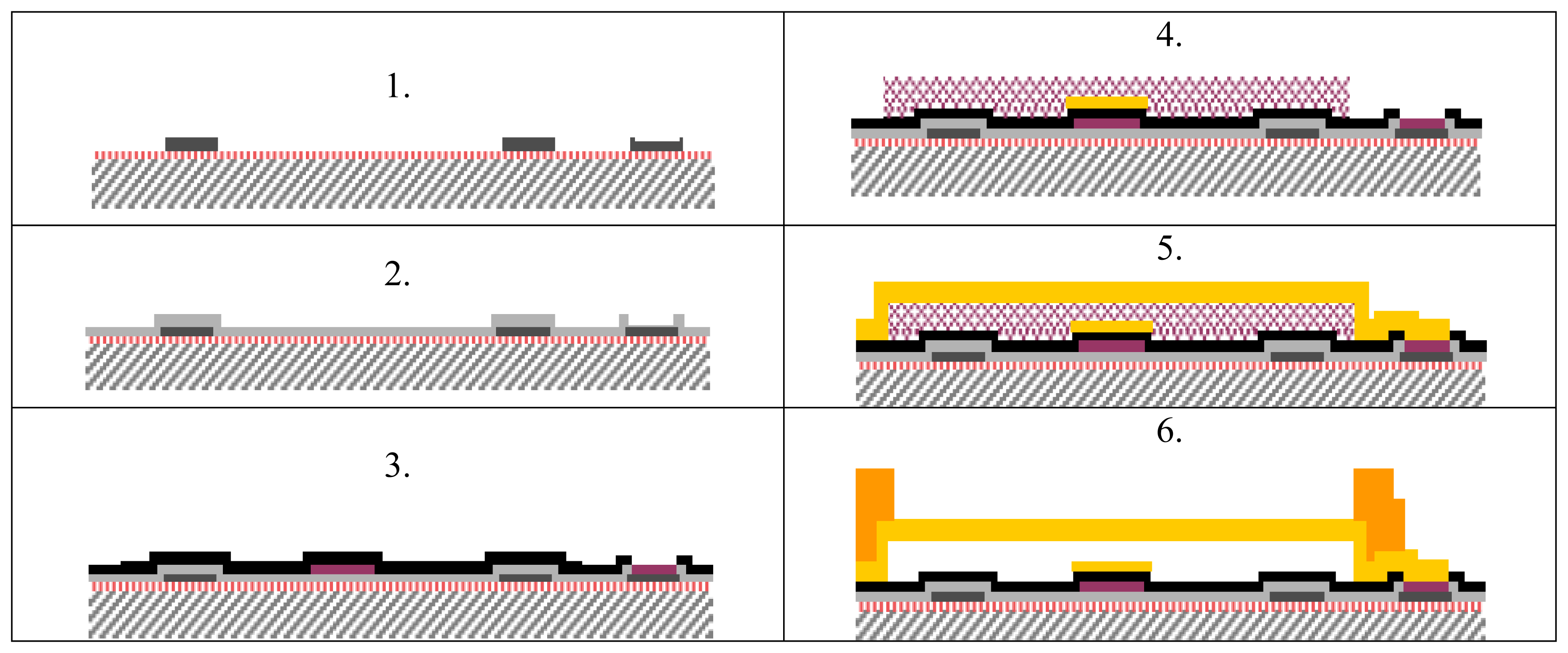
2. Fabrication process and specimen's geometry description

The specimens used for this work were prepared at the ITC-IRST research center (Trento, Italy), using the RF Switch (RFS) Surface Micromachining process, widely described in [17,18]. The process can be summarized in the following steps (Figure 1):
  • At first a 1000 nm thick thermal field oxide is grown at 975°C in a wet ambient on a silicon wafer, then a nitrogen annealing at the same temperature is performed. A 630 nm thick polysilicon layer employed for resistors and for actuation lines is deposited by LPCVD and subsequently patterned through dry etching.
  • A 300 nm thick silicon oxide is deposited at 718°C, also by LPCVD process and via-holes are opened through dry etching.
  • A multi-layer metal for signal lines is sputtered and subsequently patterned by dry etching. Temperature profile: Ti(30nm): 400°C; TiN(50 nm): 400°C; Al/Si+Ti(410/60 nm): ambient temperature; TiN(80 nm): 300°C. A 100 nm thick oxide layer is then deposited at 430°C. In order to define via-holes for opening contacts or to uncover the multimetal line oxide removal is defined with a mask by dry etching.
  • A 150 nm gold layer is deposited by PVD and patterned through wet etching. A 3 μm thick sacrificial photoresist layer is deposited and patterned.
  • A 1.3 μm thick gold layer is electroplated at 52°C employing a chromium-gold PVD adhesion layer, called seed layer. This is the suspended/movable part of the devices.
  • The last deposition step is another gold layer deposited at 52°C used to reinforce the anchors and the suspended parts of the structures. Finally, the structure release is obtained by ashing the sacrificial layer through plasma oxygen etching. At the end of the process a sintering is performed at 190°C.
The seed layer is employed to improve adhesion of gold with substrate; as an undesired consequence, poor thermal stability on gold film was verified because of the natural tendency of Cr to diffuse to the film surface at higher temperatures [17]. It was found that chromium readily diffuses through the grain boundaries of polycrystalline films to the surface during heating and oxidizes to form Cr2O3. This diffusion process can be quite extensive, with complete depletion of chromium adhesive layer and formation of channelled grain boundaries that are occupied with Cr2O3 and eventually formation of single crystals of Cr2O3 at surface. The chromium transport may manifest itself in development of undesirable characteristics, such as decrease in electrical conductivity and generation of internal stress. Residual stresses vary along the beam thickness because of the difference on percentage of diffused chromium.
Another feature considered as an origin of internal stresses within the gold beam is the difference in the coefficient of thermal expansion (CTE) between the gold beam and the photoresist sacrificial layer [2]. This introduces a stress gradient for any temperature variation during the process. Because the sacrificial layer expands at a faster rate than the gold above it, the beam is put into a state of tension at the photoresist/gold interface. The result is a tendency to creep that leads to a significant deformation of the structure.
A stress characterization was made by Margesin [18] on gold layers produced with the same micromachining process; a range of stresses varying from tensile to compressive was obtained while stress was evaluated as a function of current density and of the bath temperature employed during the fabrication process.
The structures tested in this work were produced on two different wafers, in the first one (set 1, 2, 3) beams of increasing length are grouped in sets. In the second wafer (set 4, 5, 6) each set is composed by identical beams but thickness varies from one set to the other. Experimental images of the specimen were analyzed on the basis of the IRST fabrication process technical memo in order to extrapolate a simplified profile, being the real profile quite irregular (Figure 2).

3. Measurement methods and experimental results

Frequency shift measures were preceded by accurate profilometric measures in order to know with high precision the dimensions of the specimen. Both kinds of measures were performed with the Fogale Zoomsurf 3D optical profiling system (Figure 3). This system is based on non-contact optical interferometry [19]: the recorded light intensity is detected by a CCD pixel as a function of the specimen height, thus defining either the profile of the monitored specimen or its vertical position. The maximum lateral resolution is similar to the one of conventional optical microscopes (diffraction limited, 0.6 μm with a 20X objective), while the vertical resolution may reach 0.1 nm.

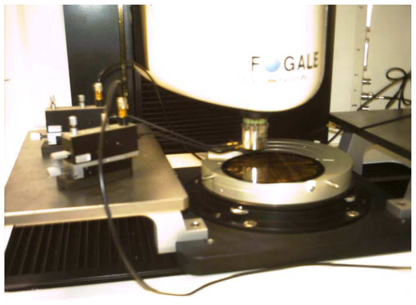
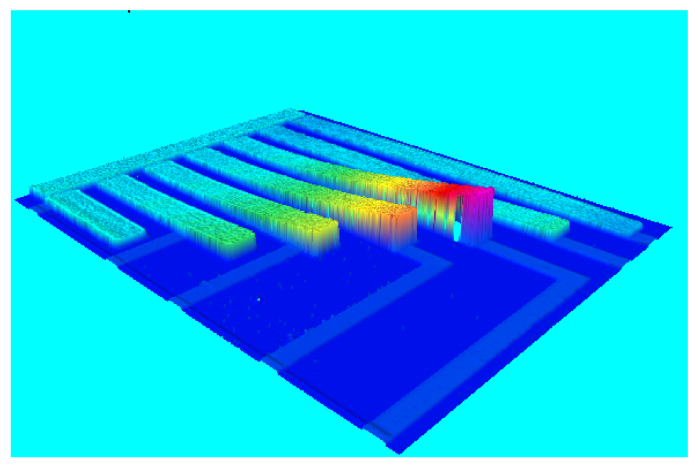
3.1. Profilometry measurements

Experimental images were treated with the Fogale 3D viewer software, which permitted the application of filters, the removal of the tilt and the calculation of mean values for each dimension. The thickness value was measured when the beam was at pull-in; gap values were obtained by subtracting to the height of the tip at 0 Volt the vertical beam deflection u and the previously measured thickness value.
In Tables 1 and 2 the main experimental dimensions of the microbeams are reported. Mean values were obtained considering the three sets of beams available. The high ratio between width and air-gap leads to exclude an influence of the three-dimensional nature of the electric field, so that the fringing-field effect can be ignored. Geometrical nonlinearity can be excluded due to the high ratio between length and air-gap [20]; this means that strains and displacements are considered small. In a FEM analysis it is possible to assume that geometry of the elements remains basically unchanged in the loading process and that strains can be approximated by a first-order linear form [21].
Deflection towards the top was observed in almost all the specimens (Figure 4). This deformation is caused by stress gradient, i.e. the stress difference that a deposited layer exhibits at its bottom and top surface. The causes are probably diffusion of the chromium of the seed-layer in the gold and difference of the CTE between gold beam and photoresist. Increase of deflection with beam length was observed, as decrease with beam thickness.

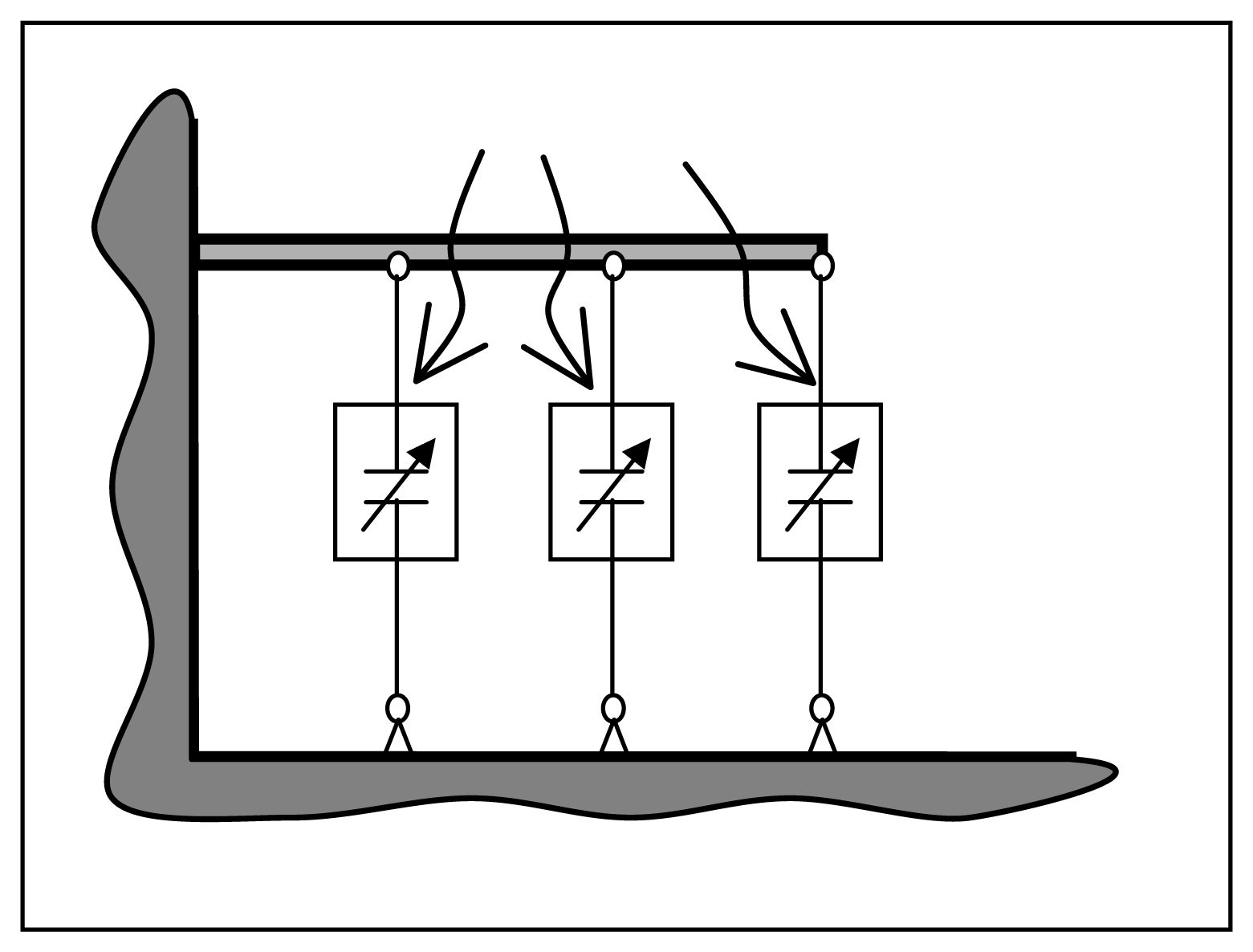
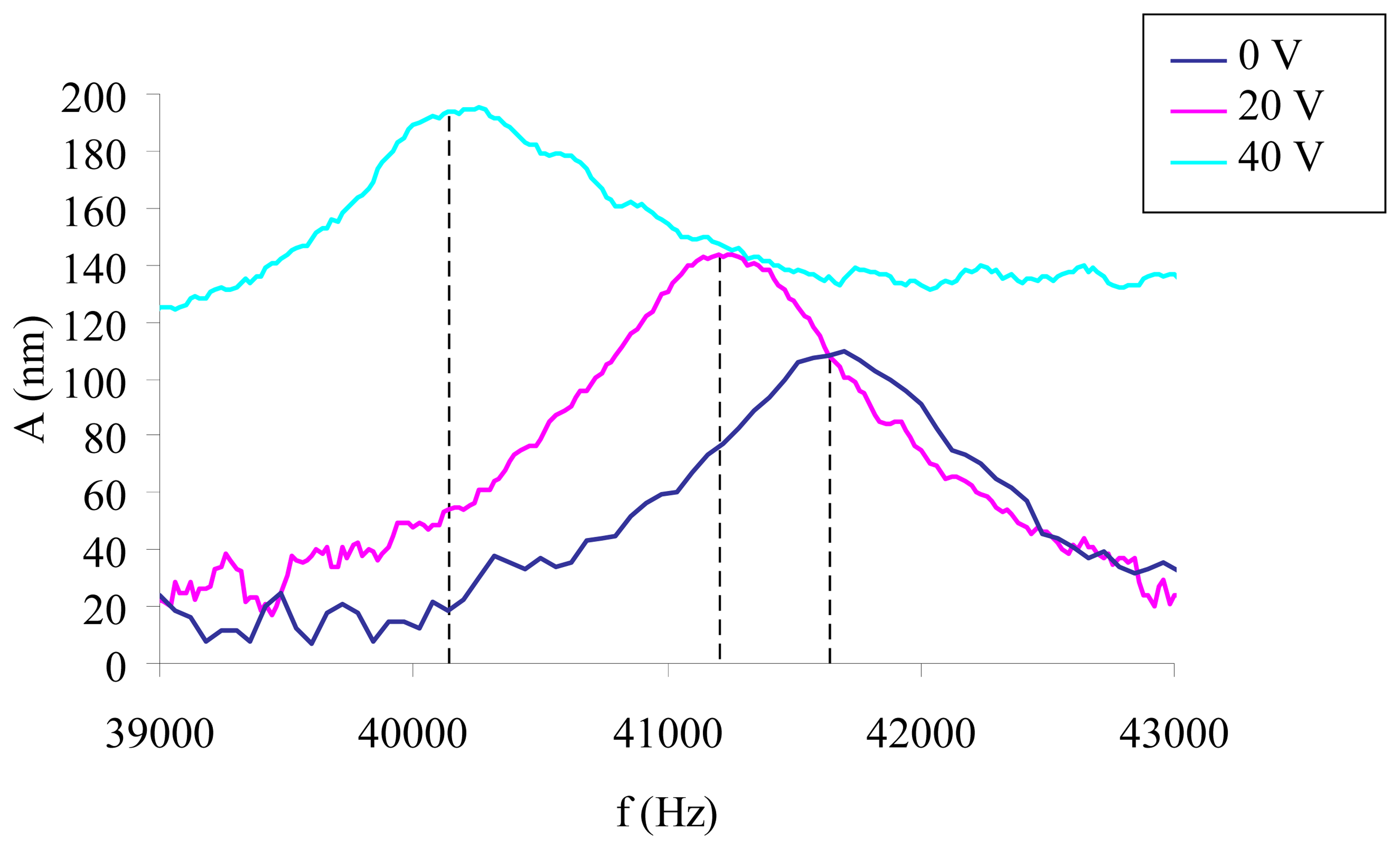
3.2. Out of plane vibration measurements

The vibration of the microbeams is obtained by the electromechanical action induced by an electric field applied between the suspended structure and the ground. The profiling system is equipped with a power supplier capable of provide up to 200 Volt; adjustable needles assure connection between power supplier and circuit. These are mounted on the ProbeHeads PH100 Suss, which have a mobile arm and a pivot magnetically fixed on the work plane of the instrument (Figure 3). The needle tip is manually driven upon the connection pad on the structure by means of three screws, controlling the motion along the three directions.
Tests were performed by applying a positive voltage VG to the suspended structure and a negative voltage to the ground. This voltage has a dc and an ac component
V G = V d c + V a c sin ( 2 π f T )
Vdc and Vac are values of the dc and ac components of the applied voltage, f is the excitation frequency and T the time. Vac was maintained at low values if compared with Vdc, in order to investigate the system behaviour around the electrostatic equilibrium position. This allowed neglecting non-linearity due to the electrostatic/structural coupling while building numerical models.
With the Fogale Zoomsurf 3D it is possible to obtain the frequency spectrum between 100 Hz and 2 MHz, applying the phase shifting interferometry technique [22], based on the measure of interference fringes phase, as shown in the spectrum graph (Figure 5). A square portion located on the tip of the cantilevers is selected as measurement spot. The increase of the dc voltage at constant ac voltage brings the system to appreciable increase of amplitude and reduction of the natural frequency. The effect can be visualized with a shift on the left of the resonance peak on the spectrum graph (Fig. 5). Frequency shift was measured until the reaching of pull-in, which appeared strongly dependent on the beam curvature.

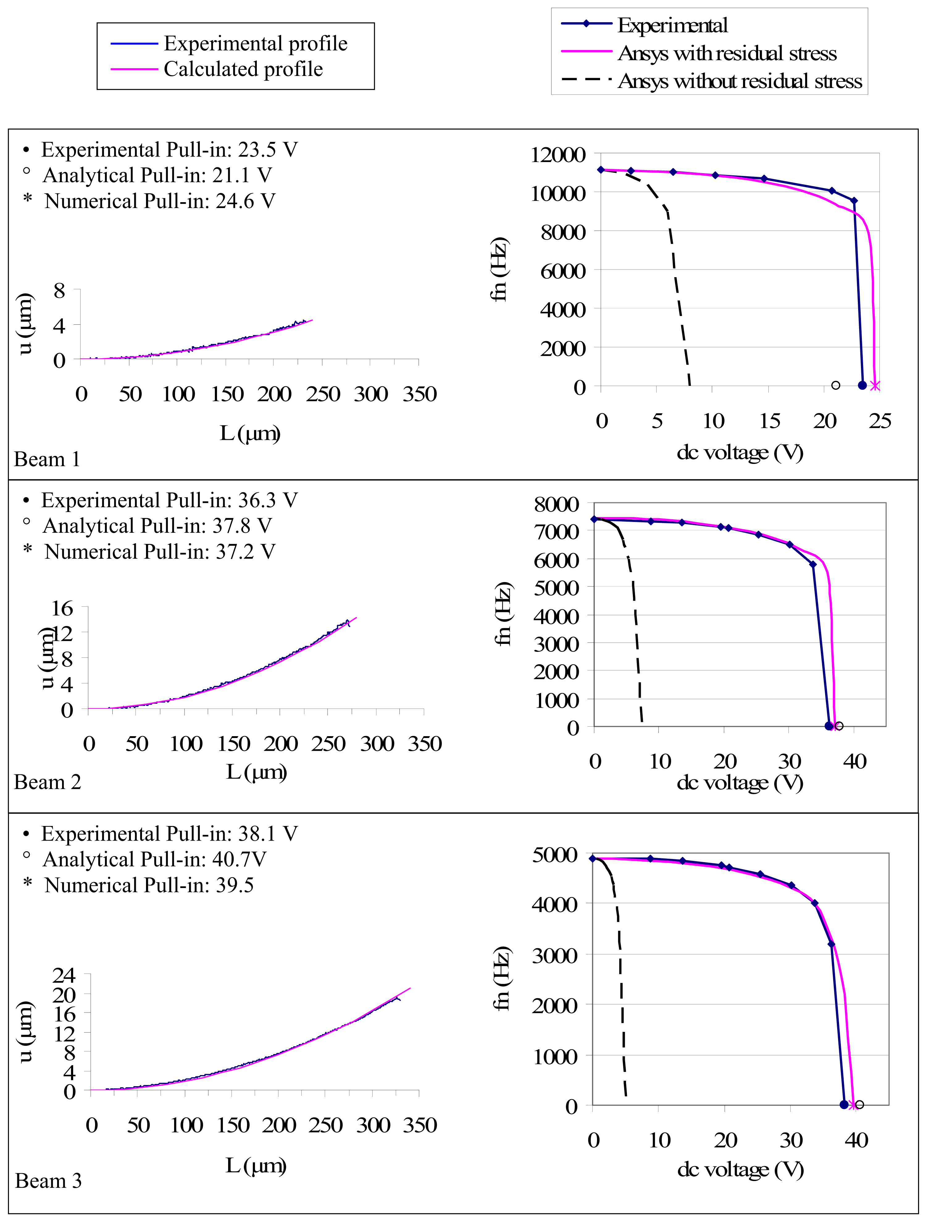
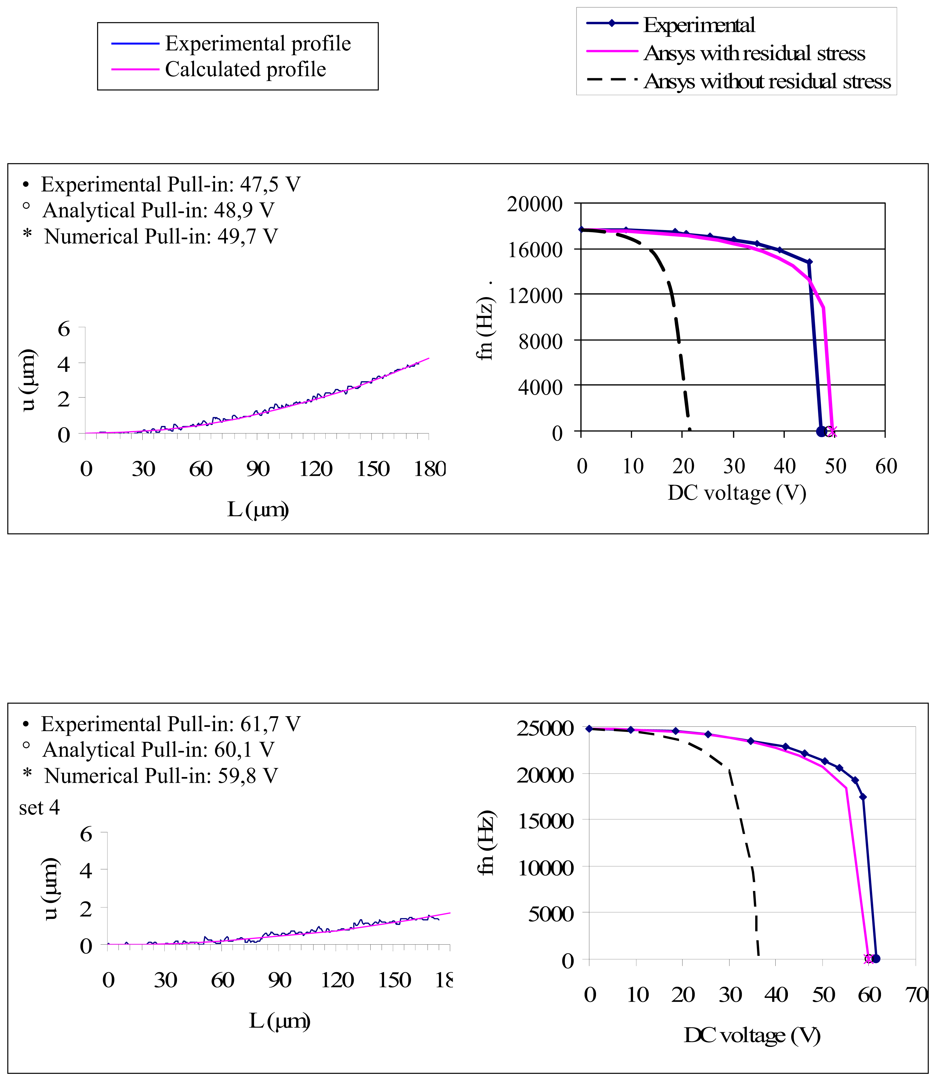
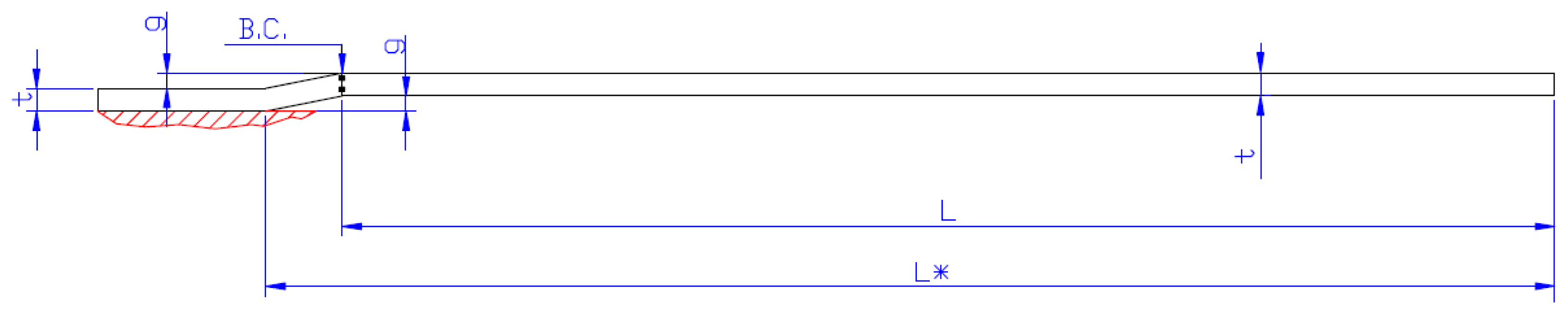
4. Frequency shift: analytical models and residual stress evaluation

4.1. Analytical models

In order to evaluate the effect of residual stresses an analytical formulation was considered: the stress function σ(z) can be written as
σ ( z ) σ 0 + σ z ( z t / 2 )
where z ∈ [−t/2,t/2] is the coordinate along the thickness with origin on the symmetry plane, σ0 is the planar constant stress and σz the coefficient of linear stress variation in z direction. The general uniaxial residual stress field in a thin film is represented by a polynomial; in this first approximation σ0 represents the cumulative effect of all the symmetric polynomial terms and σz represents the influence of the gradient stress anti-symmetric functions [23].
Stress gradient Ω is defined as follows:
Ω = d σ ( z ) d z = σ z t / 2
When a micro-machined cantilever is fabricated by removing the supporting substrate of the film, traction at the film-substrate interface is removed, and the structure becomes free to deform out-of-plane following the relief of the internal stress: σ(z) is released producing a bending moment Mb
M b = t / 2 t / 2 w σ ( z ) zdz = w [ σ 0 z 2 2 + Ω z 3 3 ] t / 2 t / 2 = w Ω t 3 12
On the assumption that the bending angle of cantilever is small, the linear differential equation that relates the bending moment to the vertical deflection u is
M b E I = d 2 u d x 2 = c
where E is the elastic modulus, I inertia moment of beam section, I = wt3/12, c is the curvature. Assuming that Mb is uniform along the x-axis, the integration of Equation (5) with respect to x is
u = M b 2 E I x 2 + A 1 x + A 0
where:
d u d x ( 0 ) = 0 A 1 = 0 u ( 0 ) = 0 A 0 = 0
The first assumption in (7) means to neglect the additional beam deflection induced by planar stress in the anchor point. From the exam of experimental images this hypothesis results acceptable, but it can eventually be removed by collocating A1= A10z) [23].
The deflection of the end of the cantilever uL is obtained using Equation (4) in Equation (6)
u L = L 2 2 E I M b = Ω L 2 2 E
Substituting Equation (4) in Equation (5), a relation between curvature and stress gradient is obtained:
Ω = c E
To obtain an analytical model of the cantilever bending, g(x) is introduced as a variable gap, defined using equations (5) and (6)
g ( x ) = u ( x ) + g 0 = c 2 x 2 + g 0
c = 2 u L 2 is calculated from equations (5) and (10) using experimental data, g0 is the gap in ideally flat conditions, also known from specimen profilometry. In Figures 7 and 8 a comparison between experimental and analytically calculated profiles of the upper side of the microbeams is presented. In Figure 7 specimens of wafer 1 are disposed by increasing length while in Figure 8 specimens of wafer 2 are disposed by increasing thickness.

4.2. Numerical models

Two different 2-D models were implemented with ANSYS™, assuming ideally clamped conditions in the microbeam. The constraint was applied at the beginning of L dimension (B.C. in Figure 2), neglecting the anchoring on the substrate. This assumption is possible due to the high ratio between length and width of the beam [24]. Electrostatic field fringing effect was neglected due to the high ratio between width and air-gap [25], so that implementation of 3-D models was not necessary.
Particular attention to the fringing field effect of MEMS beam has been paid by authors in previous works, in particular extensively modelling and experimental identification of non-linearity of the electrostatic coupling has been done in the case of static behaviour of MEMS cantilevers [20, 21].
The numerical modelling and the results included in the present paper refer only to the structural domain, in this case the dimension of the beam and the experimentally measured Q-factor allow disregarding the effect of dynamic fluid interaction around the structure. Specific investigation of fluid-structure coupling in MEMS using FEM multi-physics models and experimental measurements was carried out by authors in other works [26] in the case of larger plates with holes. In both models 50 BEAM4 elements were used to reproduce the structure while 1-D transducer TRANS126 elements were connected at each structural node. An electro-mechanical coupling was thus realized between a distributed mechanical domain and a lumped electrical domain. (Figure 6). TRANS126 element has up to two degrees of freedom at each node: translation in the nodal x, y or z direction and electric potential. This makes possible to represent the capacitive response of a structure to a movement in one direction [27]. In the presented case indefinite capacitor theory was used since fringing field along the lateral edges of the structure was neglected, and the capacity characteristic of the elements was set as real constant by imposing the value of C0 obtained with the following formula:
C 0 = ε 0 w l n
where n is the number of TRANS126 elements used in the model. A potential difference was imposed to the nodes connected to the positive electrode, and all the degrees of freedom, both translation and voltage, were set to zero for the nodes connected to the ground.
For frequency behaviour simulation, the routine is first to proceed with a static analysis with the pre-stress option turned on and then perform a modal analysis. The included pre-stress is responsible for the effects of the applied voltage on the system frequency characteristic and, in the first model, for the residual stress inclusion. The program outputs are mechanical displacements and eigenfrequencies with incorporated electrostatic effects.
A first model was implemented by applying on the free tip of the cantilever a bending moment derived from Equation (4):
M b = cEI = 2 u L 2 E I
Equation (10) was used in the second model to build a beam with increasing gap: the distance between the two nodes of each TRANS126 element was calculated so that the structure could have a parabolic profile. The adopted Young modulus of gold was 98.5 GPa, while for density the value 19.3 e-15 Kg/μm3 was used [18].
Stress gradients for each single specimen were calculated from Equation (9) and are reported in Tables 1 and 2; from the post-processing of the results of implemented ANSYS™ models, the same value of stress gradient was encountered. Stress gradient appears to increase with length while inverse proportionality can be noticed between thickness and curvature of the beam; in the case of 4.8 thick cantilevers no curvature is detected, this means that stress gradient is very low. A mean value of stress gradient for each available length and thickness was calculated.
In Figures 7 and 8, beside specimen profiles, experimental frequency shift curves are compared with the curves calculated with implemented ANSYS™ models, considering the case of ideally flat beam and the case of curled beam.
From Figure 7 it can be observed that an increase in length doesn’t provide a decrease in pull-in tension in presence of residual stress as would be expected from Senturia-Osterberg formulation (13). The initial curling creates a higher average distance between suspended structure and ground so that pull-in tensions result higher. On the contrary, in the case of flat beam, inverse proportionality between length and pull-in tension is respected. From Figure 8 it can be observed that proportionality between thickness and pull-in tension is respected also in presence of residual stress.
The Senturia-Osterberg formulation [28] was used to analytically calculate pull-in tension in order to evaluate in advance the measurement range of each specimen. This simplified the execution of the experiments and the implementation of the numerical models.
V PI = 4 γ 1 g 0 3 t 3 E ε 0 L 4 γ 2 ( 1 + γ 3 g 0 w )
where γ1, γ2, γ3 are fitting parameters depending on the constraints. In the case of cantilever γ1=0.07, γ2=1,γ3=0.42.
Gupta's work [29] was followed to include the curvature of the beams in pull-in tension calculation: with the finite-difference method a corrective coefficient fc formulation was encountered by stopping at the second term a Taylor series expansion. It's thus possible to pass from Vpi from Equation (13) to Vpi,c as follows
f c = V P I , c V P I 1 + 1 2 ( L 2 g 0 R c )
Where Vpi is the pull-in voltage of a flat cantilever, Vpi,c is the pull-in voltage of a curled cantilever, Rc is curvature radius, calculated as the inverse of curvature c.
The ANSYS™ beam models used for frequency shift calculation were modified to implement an algorithm for the accurate calculation of the pull-in voltage value; the Voltage Iteration Method[30] was adopted. This consists in an iterative approach to the pull-in voltage with decreasing voltage increments. At each iteration the static equilibrium deformation is calculated for the applied voltage. If the deformation calculation converges, it is concluded that the applied voltage is below the pull-in value. On the other hand, if the calculated deformation fails to converge it is concluded that the applied voltage is higher than the pull-in value. The interval between these two limits is continuously decreased until the voltage interval is smaller than a predetermined accuracy [30].
The obtained pull-in values were used to complete the numerical frequency shift curves and were compared with analytical results from formulas (13), (14) and with experimental values (Figures 7, 8). Good adherence was encountered for the majority of specimen in all cases of dimensions and hence of curvature; the effectiveness of the models was hence confirmed.

5. Conclusions

In this study experimental frequency shift curves were obtained through optical interferometric measures on vibrating microcantilevers, the lowering of natural frequency with the increase of electrostatic force was detected.
The experimental results were compared with FEM solutions from reduced order models using a specific capacitive element of ANSYS™ to model the electrostatic field. The residual stress effect on the structures was included in the models being necessary to determine the initial upward curvature and the correct pull-in tension value. The presence of stress gradient strongly influenced the frequency shift curve and the pull-in. The structures tested in this work were produced on two different wafers, in the first one beams of increasing length are grouped in sets. In the second wafer each set is composed by identical beams but thickness varies from one set to the other. The adherence with experimental measures varied from specimen to specimen, the biggest discrepancies appeared near pull-in, due to the high variability of this parameter in measures.
In the studied cases of cantilever beams the stress gradient is taken into account in the FEM model simply by reproducing the measured initial curvature and thus obtaining frequency shift curves in good agreement with the measured curves. The stress gradient revealed by the curvature measurement slightly change in the same wafer due to the cantilever length. In the second wafer the stress gradient revealed by the curvature tends to zero by increasing the cantilever thickness.
In all these different cases the good agreement of the numerical versus experimental frequency shift graph shows how the stress gradient model works successfully. Among the causes of the stress gradient the experimental results of the present work may confirm a combined effect due to both chromium diffusion and the difference in the coefficient of thermal expansion (CTE) between the gold beam and the layer. The latter introduces a stress gradient for any temperature variation during the process that decreases with the thickness increase as confirmed in the frequency shift graph. The method presented in this paper can be useful both for identify the process residual stress gradient and to numerically evaluate the optimal thickness for the process.

Acknowledgments

This work was partially funded by the Italian Ministry of University, under grant PRIN-2005/2005091729. Specimens were built by ITC-IRST research center (Trento, Italy). Authors thank all above involved institutions.

References

  1. Chung, K.; Fang, Y. J.; Cheng, C. M.; Hong, Y. Z.; Wang, C. H. Effect of seed layer stress on the fabrication of monolithic MEMS microstructures. Microsyst. Technol. 2007, 13, 299–304. [Google Scholar]
  2. Stanec, J. R.; Smith, C. H., III; Chasiotis, I.; Barker, N. S. Realization of low-stress Au cantilever beams. J. Micromech. Microeng. 2007, 17, N7–N10. [Google Scholar]
  3. Elbrecht, L.; Storm, U.; Catanescu, R.; Binder, J. Comparison of stress measurement techniques in surface micromaching. J. Micromech. Microeng. 1997, 7, 151–154. [Google Scholar]
  4. Fang, W.; Wickert, J.A. Post buckling of micromaching beams. J. Micromech. Microeng. 1994, 4, 116–122. [Google Scholar]
  5. Fang, W.; Wickert, J.A. Determining mean and gradient residual stresses in thin films using micromachined cantilevers. J. Micromech. Microeng. 1996, 6, 301–309. [Google Scholar]
  6. Chung, C.K.; Lin, C.J.; Wu, L.H.; Fang, Y.J.; Hong, Y.Z. Selection of mold materials for electroforming of monolithic two-layer microstructure. Microsyst. Technol. 2004, 10, 467–471. [Google Scholar]
  7. Kim, J.W.; Yamagata, Y.; Morita, S.; Moriyasu, S.; Ohmori, H.; Higuchi, T. A study on the fabrication of multi-layer microstructure using ELID grinding and the thick photoresist technology. Key Eng. Mater. 2003, 238–239, 19–22. [Google Scholar]
  8. Zhang, L.X.; Zhao, Y.P. Electromechanical model of RF MEMS switches. Microsyst. Technol. 2003, 9, 420–426. [Google Scholar]
  9. Nicu, L.; Temple-Boyer, P.; Bergaud, C.; Scheid, E.; Martinez, A. Energy study of buckled micromachined beams for thin-film stress measurements applied to SiO2. J. Micromech. Microeng. 1999, 9, 414–421. [Google Scholar]
  10. Laconte, J.; Iker, F.; Jorez, S.; Andrè, N.; Proost, J.; Pardoen, T.; Flandre, D.; Raskin, J.P. Thin films stress extraction using micromachined structures and wafer curvature measurements. Microelectron. Eng. 2004, 76, 219–226. [Google Scholar]
  11. Baek, C.W.; Kim, Y.K.; Ahn, Y.; Kim, Y.H. Measurement of the mechanical properties of electroplated gold thin films using micromachined beam structures. Sens. Actuat. A 2005, 117, 17–27. [Google Scholar]
  12. Lee, W. S.; Kim, B. K.; Cho, J. H.; Youn, S. K.; Kwon, K. C. Frequency-shifting analysis of electrostatic tunable micromechanical actuator. J. Model. Simul. Microsyst. 2001, 2, 83–88. [Google Scholar]
  13. Brusa, E.; De Bona, F.; Gugliotta, A.; Somà, A. Modelling and prediction of the dynamic behaviour of microbeams under electrostatic load. Analog Integr. Circ. S. 2004, 40, 155–164. [Google Scholar]
  14. Van Der Poel Filho, C. J.; Gugliotta, A.; Somà, A.; Pavanello, R. Dynamic Identification of MEMS by Eigensensitivity and Newmark Simulation. Analog Integr. Circ. S. 2005, 44, 155–162. [Google Scholar]
  15. Brusa, E.; De Bona, F.; Della Schiava, A.; Somà, A. Model synthesis of structural dynamics for electrostatic microactuators. Presented at European micro and nano systems 2004, Paris, 20-21 October, 2004.
  16. Zhang, Y.; Zhao, Y. An effective method of determining the residual stress gradients in a micro-cantilever. Microsyst. Technol. 2006, 12, 357–364. [Google Scholar]
  17. Subhadeep, K.; Bagolini, A.; Margesin, B.; Zen, M. Stress and resistivity analysis of electrodeposited gold films for MEMS application. Microelectron. J. 2006, 37. [Google Scholar]
  18. Margesin, B.; Bagolini, A.; Guamieri, I.; Giacomozzi, F.; Faes, A. Stress characterization of electroplated gold layers for low temperature surface micromachining. Presented at Symposium on Design Test, Integration & Packaging of MEMS-MOEMS, Mandelieu-La Napoule, France, 5-7 May, 2003.
  19. Zoomsurf 3D User manual Version 1.3; Fogale Nanotech: Nimes, France.
  20. Ballestra, A.; Brusa, E.; Munteanu, M.G.; Somà, A. Experimental characterization of the static behaviour of microcantilevers electrostatically actuated. Presented at Symposium on Design Test, Integration & Packaging of MEMS-MOEMS, Stresa, Italy, 25-27 April 2007.
  21. Collenz, A.; De Bona, F.; Gugliotta, A.; Somà, A. Large deflections of microbeams under electrostatic loads. J. Micromech. Microeng. 2004, 14, 365–37. [Google Scholar]
  22. Petitgrand, S.; Yahiaoui, R.; Danaie, K.; Bosseboeuf, A.; Gilles, J. P. 3D measurement of micromechanical devices vibration mode shapes with a stroboscopic interferometric microscope. Optics and Lasers in Engineering 2001, 36(2), 77–101. [Google Scholar]
  23. Fang, W.; Wickert, J.A. Determining mean and gradient residual stresses in thin films using micromachined cantilevers. J. Micromech. Microeng. 1996, 6. [Google Scholar]
  24. Tibeica, C.; Voicu, R.; Bazu, M.; Ilian, V.E.; Vasilache, D.; Galateanu, L.; Pons, P.; Yacine, K.; Flourens, F. Analytical VS. Computational approach of the pull-in voltage of electrostatically actuated micro-bridges. 0-7803-9214-0/05. IEEE 2005. [Google Scholar]
  25. O’Mahony, C.; Hill, M.; Duane, R.; Mathewson, A. Analysis of electromechanical boundary effects on the pull-in of micromachined fixed-fixed beams. J. Micromech. Microeng. 2003, 13, S75–S80. [Google Scholar]
  26. Somà, A.; De Pasquale, G. Identification of test structures for Reduced Order Modeling of the squeeze film damping in MEMS. Presented at Symposium on design, test, integration and packaging of mems/moems, 2007, Stresa, Italy, 25-27 April, 2007.
  27. .
  28. Osterberg, P.M.; Senturia, S.D. M-Test: a test chip for MEMS material property measurement using electrostatically actuated test structures. J. Microelectromech. Syst. 1997, 6(2). [Google Scholar]
  29. Gupta, K. J. Electrostatic Pull-in Test Structure Design for in-situ Mechanical Property Measurements of Microelectromechanical Systems (MEMS). Ph.D. dissertation, 1998. [Google Scholar]
  30. Nemirovsky, Y.; Bochobza-Degani, O. A methodology and model for the pull-in parameters of electrostatic actuators. J. Microelectromech. Syst. 2001, 10(4). [Google Scholar]

Abbreviations

c
curvature
E
elastic modulus
f
exitation frequency
fc
corrective coefficient for pull-in tension
fn
natural frequency
g
air-gap
g0
initial gap
gm
medium gap
I
inertia moment of beam section
L
effective length
Lc
total length
m
mass
Mb
bending moment
Rc
curvature radius
S
surface
t
thickness
Vac
ac voltage
Vdc
dc voltage
w
width
u
vertical beam deflection
z
vertical coordinate along the thickness
ε0
dielectric constant
σ0
planar constant stress
σz
coefficient of linear stress variation
Ω
stress gradient
Figure 1. The RF Switch (RFS) Surface Micromachining process.
Sensors 08 00767f1
Figure 2. Schematic cantilever beam profile with geometrical dimensional parameters.
Sensors 08 00767f2
Figure 3. Experimental set-up on the Fogale Zoomsurf 3D.
Sensors 08 00767f3
Figure 4. Specimen set: 3D image obtained with the Zoomsurf Fogale 3D profiler.
Sensors 08 00767f4
Figure 5. Experimental frequency spectrum of a microbeam with Vac=4.5V and three different values of DC voltage: 0V: fn=41640 Hz, Q= 43.4; 20V: fn=41230 Hz, Q=38.2; 40V: fn=40110, Q=35.9. Q factor was calculated with the half power method.
Sensors 08 00767f5
Figure 6. Sketch of the Ansys model.
Sensors 08 00767f6
Figure 7. Upper profile and frequency shift variation in cantilever beams of set 3.
Sensors 08 00767f7
Figure 8. Upper profile and frequency shift variation of cantilever beams of set 4 (nominal thickness 1.8 um), set 5 (nominal thickness 3 um) and set 6 (nominal thickness 4.8 um).
Sensors 08 00767f8
Table 1. Experimental measures and stress gradient in first wafer.
g (μm)t (μm)L (μm)u (μm)c (μm-1)Ω (MPa/μm)
specimen1
set13.01.78242.43.811.30E-0412.8
set23.01.68245.05.301.77E-0417.4
set33.01.75240.04.671.62E-0416.0

mean value3.01.73±0.05242.5±2.54.59±0.741.56E-0415.4±2.3

specimen2
set13.01.84288.513.433.23E-0431.8
set23.01.71289.413.613.25E-0432.0
set33.01.72293.312.232.84E-0428.0

mean value3.01.76±0.06290.6±2.713.09±0.693.11E-0430.6±2.0

specimen3
set13.01.91340.119.143.31E-0432.6
set23.01.59343.818.853.19E-0431.4
set33.01.55340.114.112.44E-0424.0

mean value3.01.68±0.18341.3±1.817.37±2.512.98E-0429.3±4.3
Table 2. Experimental measures and stress gradient in second wafer.
g (μm)t (μm)L (μm)u (μm)c (μm-1)Ω (MPa/μm)
specimen1
set43.01.78192.84.162.23E-0422.0
set53.01.77191.44.652.53E-0424.9
set63.01.74189.64.232.35E-0423.1

mean value3.01.76±0.02191.3±1.64.352.37E-0423.3

specimen2
set43.02.41191.92.691.46E-0414.4
set53.02.26192.12.101.14E-0411.2
set63.02,31192.12.551.38E-0413.6

mean value3.02.33±0.07192.0±0.22.451.32E-0413.7

specimen3
set43.04.31189.9000
set53.04.40191.5000
set63.04.37190.5000

mean value3.04.36±0.04190.6±0.8000

