Review

A Review on the Electrochemical Sensors and Biosensors Composed of Nanowires as Sensing Material

Department of Chemical Engineering and Biotechnology, National Taipei University of Technology, No.1, Section 3, Chung-Hsiao East Road , Taipei 106, Taiwan (ROC)
*
Author to whom correspondence should be addressed.
Sensors 2008, 8(1), 290-313; https://doi.org/10.3390/s8010290
Submission received: 29 December 2007 / Accepted: 14 January 2008 / Published: 21 January 2008

Abstract

:
The development and application of nanowires for electrochemical sensors and biosensors are reviewed in this article. Next generation sensor platforms will require significant improvements in sensitivity, specificity and parallelism in order to meet the future needs in variety of fields. Sensors made of nanowires exploit some fundamental nanoscopic effect in order to meet these requirements. Nanowires are new materials, which have the characteristic of low weight with extraordinary mechanical, electrical, thermal and multifunctional properties. The advantages such as size scale, aspect ratio and other properties of nanowires are especially apparent in the use of electrical sensors such as electrochemical sensors and in the use of field-effect transistors. The preparation methods of nanowires and their properties are discussed along with their advantages towards electrochemical sensors and biosensors. Some key results from each article are summarized, relating the concept and mechanism behind each sensor, with experimental conditions as well as their behavior at different conditions.

1. Introduction

Sensors are the devices, which are composed of an active sensing material with a signal transducer. The role of these two important components in sensors is to transmit the signal without any amplification from a selective compound or from a change in a reaction. These devices produce any one of the signals as electrical, thermal or optical output signals which could be converted in to digital signals for further processing. One of the ways of classifying sensors is done based on these output signals. Among these, electrochemical sensors have more advantage over the others because; in these, the electrodes can sense the materials which are present within the host without doing any damage to the host system. On the other hand, sensors can be broadly classified in to two categories as chemical sensors and biosensors. The biosensors can be defined in terms of sensing aspects, where these sensors can sense biochemical compounds such as biological proteins, nucleotides and even tissues [1-3]. Within these sensors, the active sensing material on the electrode should act as a catalyst and catalyze the reaction of the biochemical chemical compounds to obtain the output signals [4,5]. The combination of these two different ways of classifications has given rise to a new type of sensors which are called electrochemical biosensors, where the electrochemical methods are applied for the construction and working of a biosensor [6-8].
The selection and development of an active material is a challenge. The active sensing materials maybe of any kind as whichever acts as a catalyst for sensing a particular analyte or a set of analytes. The recent development in the nanotechnology has paved the way for large number of new materials and devices of desirable properties which have useful functions for numerous electrochemical sensor and biosensor applications [9-13]. Basically by creating nanostructure, it is possible to control the fundamental properties of materials even without changing their chemical composition. In this way the attractive world of low dimensional systems, together with the current tendencies on the fabrication of functional nanostructured arrays could play a key role in the new trends of nanotechnology [14-16]. Further, the nanostructures can be used for both efficient transport of electrons and optical excitation, and these two factors make them critical to the function and integration of nanoscale devices [17-19]. In fact, nanosystems are the smallest dimension structures that can be used for efficient transport of electrons and are thus critical to the function and integration of these nanoscale devices. Because of their high surface-to-volume ratio and tunable electron transport properties due to quantum confinement effect, their electrical properties are strongly influenced by minor perturbations.
Recent studies have shown considerable attraction towards these nanostructures, particularly on nanowires. Generally, these kind of nanostructures could be prepared by two methods, one is by “bottom-up” approach where, the self-assembly of small sized structures form into larger structures. The other is by “top-down” approach where, the reduction of large systems down into smaller sizes to produce multifunctional nanoscale structures [20-22]. When used in biosensing devices, these nanowires have two main advantages over carbon nanotubes (CNTs). Firstly, the material properties can be more precisely controlled by manipulating the conditions during synthesis and using well-developed doping techniques. Secondly, the native oxide layer that forms on the outside of nanowires allows the use of a broad class of already well developed functionalization and blocking chemistries. In the literature, electrochemical sensor device designing, selection of suitable sensing material for suitable analyte and their wide applications are already abundant [23,24]. Among these, application of nanowires in biosensors shows the most interesting studies [25-32]. In this review, we especially interested in reporting about the biosensor devices made of nanowires as an active sensing material.

2. Synthesis of Nanowires

A good method for generating any kind of nanostructures should enable simultaneous control of the dimensions, properties, and morphology. In general, nanostructures are synthesized by promoting the crystallization of solid-state structures along one direction by various mechanisms which includes, the use of templates with nanostructure morphologies to direct the formation of nanostructures; the use of intrinsically anisotropic crystallographic structure of a solid to achieve nanowires growth; the use of a liquid/solid interface to reduce the symmetry of a seed and the use of appropriate capping agents to kinetically control the growth rates of various facets of a seed [33]. Among these, highly successful methods to obtain nanowires and nanowire arrays are by using the synthesis on templates and self assembly or self-organization processes. These processes can be further explained by means of self assembly of one material in the roughness or relief present on the solid surface; self-organization within the channels and cavities of porous material and the formation of inorganic mesoscopic material by self-assembled on surfactants organic molecules [9]. The first and most important process of this strategy is the creation of a desirable surface structure on which the nanowires growth should take place; for this goal several top-down techniques like molecular beam epitaxy, electron beam evaporation, phase-shift optical lithography and sputtering have been used [34-36].
Generally, anodization techniques are being increasingly used to create the ordered nanoporous structures which in turn being used as templates to grow functional nanowires of different species by mainly self-assembling process and electroplating techniques. By means of both anodization and electrodeposition processes, it could be possible to take control on, ordering degree, i.e., the size of crystalline single domains (up to several square micrometers); the single one dimensional structure diameter (from 15 to 200 nm) and length (from tens to thousands of nanometers); the lattice parameter of ordered arrays (between 65 and 500 nm) [9]. Brief explanations about the various template and nanowires synthesis methods and properties are given in the following sections.

2.1. Anodic Alumina Membranes (AAM)

The most interesting characteristics of these membranes is the growth of arrays of well ordered hexagonal cells with central pores parallel to each other and with a symmetry axis perpendicularly oriented to the substrate surfaces [37], allowing the highest yield of diffusion processes for those applications in which this phenomenon could be the determinant. Taking advantage of this particular property, the electrochemical growth technique either galvanostatic, potenciostatic, or a mix of both methods have been the most used procedure to obtain functionalized AAM [38-41]. Thus, AAM has become an important material in nanotechnology development within research fields such as, optoelectronic, high density magnetic storage devices and biotechnology. In these the main attention has been focused to the use of AAM as templates for self-assembly processes of very varied species for pre-determined functionality [42-45]. Recently, great advancement has been achieved in the fabrication of single crystalline nanopore arrays of AAM by using a combination of nano-imprint and lithographic techniques with a subsequent anodization process of aluminium metal and other metallic or semiconductor substrates [46,47].

2.2. AAM on Silicon Substrates

Generally, in this approach aluminium thin films are deposited on silicon wafers by using electron beam evaporation or sputtering magnetron techniques. In these cases it has been shown about the great dependence of the nanoporous alumina film morphological features on the grain size distribution of the starting aluminium thin film and on the anodization time. With an accurate control of the anodization time it could be possible to obtain the AAM on Silicon as two well defined phases, separated by a barrier layer, or replicate of the AAM nanoporous structure on the silicon surface. The advantages of this approach are the integration with silicon based electronic devices, high control of the growth processes and the possibility of getting high control on the lengths of semiconductors grown within the AAM. Other interesting advantages of this approach are the purity that can be obtained in the synthesized products and also the possibility of transferring the alumina nanoporous structure into the silicon substrate [48].

2.3. Nanoporous Anodic Titania Films

Nanoporous titania are mainly interesting for their semiconducting, sensing and biocompatible properties [49-51]. Although the experimental setup for Al and Ti anodization are practically the same, the anodization parameters such as the temperature, the electrolytes used and the efficiency of the processes for growing nanoporous titanium dioxide thin films are notably different from those used in the growth of nanoporous alumina. In addition, nanoporous alumina obtained by this process is, in general, amorphous whereas, a synthesized nanoporous titanium dioxide could undergo crystalline phases transformation by mean of single thermal treatment [52].

3. Electrical Properties of Nanowires

Electron transport properties of nanowires are very important for electrical and electronic applications as well as for understanding the unique one-dimensional carrier transport mechanism. It has been noticed that the wire diameter, wire surface condition, crystal structure and its quality, chemical composition, crystallographic orientation along the wire axis etc are important parameters, all of which influence the electron transport mechanism of nanowires. For example, the I-V characteristic studies of the Cu nanowires both at room temperature and at 4.2 K showed the linear ohmic behavior [53]. However, by oxidation when the metallic Cu nanowires has been transformed into semiconducting Cu2O nanowires and placed between two electrodes, it forms two Schottky diodes in series and in turn produces a double diode like I–V characteristic curve. It has been reported that quasi one-dimensional nanowires exhibit both ballistic and diffusive type electron transport mechanism, which depends upon the wire length and diameter. Ballistic type transport phenomena is associated with predominant carrier flow without scattering which is due to the fact that the carrier mean free path is longer than that of the wire length. Ballistic type transport mechanism is normally observed at the contact junction of nanowire and other external circuits [54,55], where the conductance is quantized into an integral multiple of 2e2/h, called the universal conductance unit (e is the electronic charge and h the Plank's constant) [53,56,57]. In the case of ballistic type transport in metallic nanowires, the conductance quantization phenomena takes place because of the fact that the nanowire diameter becomes comparable to the electron Fermi wavelength of that metal [58]. As compared to the ballistic transport mechanism, in diffusive type conduction mechanism, the carrier mean free path is smaller than that of the wire length. Therefore, various types of scattering affect the carriers and the carrier transport mechanism of nanowires becomes quite similar to that of bulk counterpart.
It is found that the conductance of nanowires strongly depends on their crystalline structure. For example, in the case of perfect crystalline Si nanowires having four atoms per unit cell, generally three conductance channels are found [59]. One- or two-atom defect, either by addition or removal of one or two atoms may disrupt the number of such conductance channel and may cause variation in the conductance. It has been observed that change in the surface conditions of the nanowires can cause remarkable change in the transport behaviour. This has been reported as the change in electrical conductivity which has been caused by the variation of the surface scattering phenomena of carriers in nanowires. This happens when the diameters of the nanowires are changed. It has also been reported that the redox molecules like cobalt phthalocyanine layer coating on the n-InP nanowires change their conductance remarkably [60]. Other reports have shown that the resistance of Pd nanowires changes by an order of magnitude due to the adsorption of hydrogen gas molecules on the wire surface.

4. Nanowires for Hydrogen and Ethanol Sensors

Various types of nanowire modified electrodes have been reported for hydrogen. However, for ethanol only one type of nanowire (ZnO) modified electrode has been reported. In the following sections, we will discuss each study in detail.

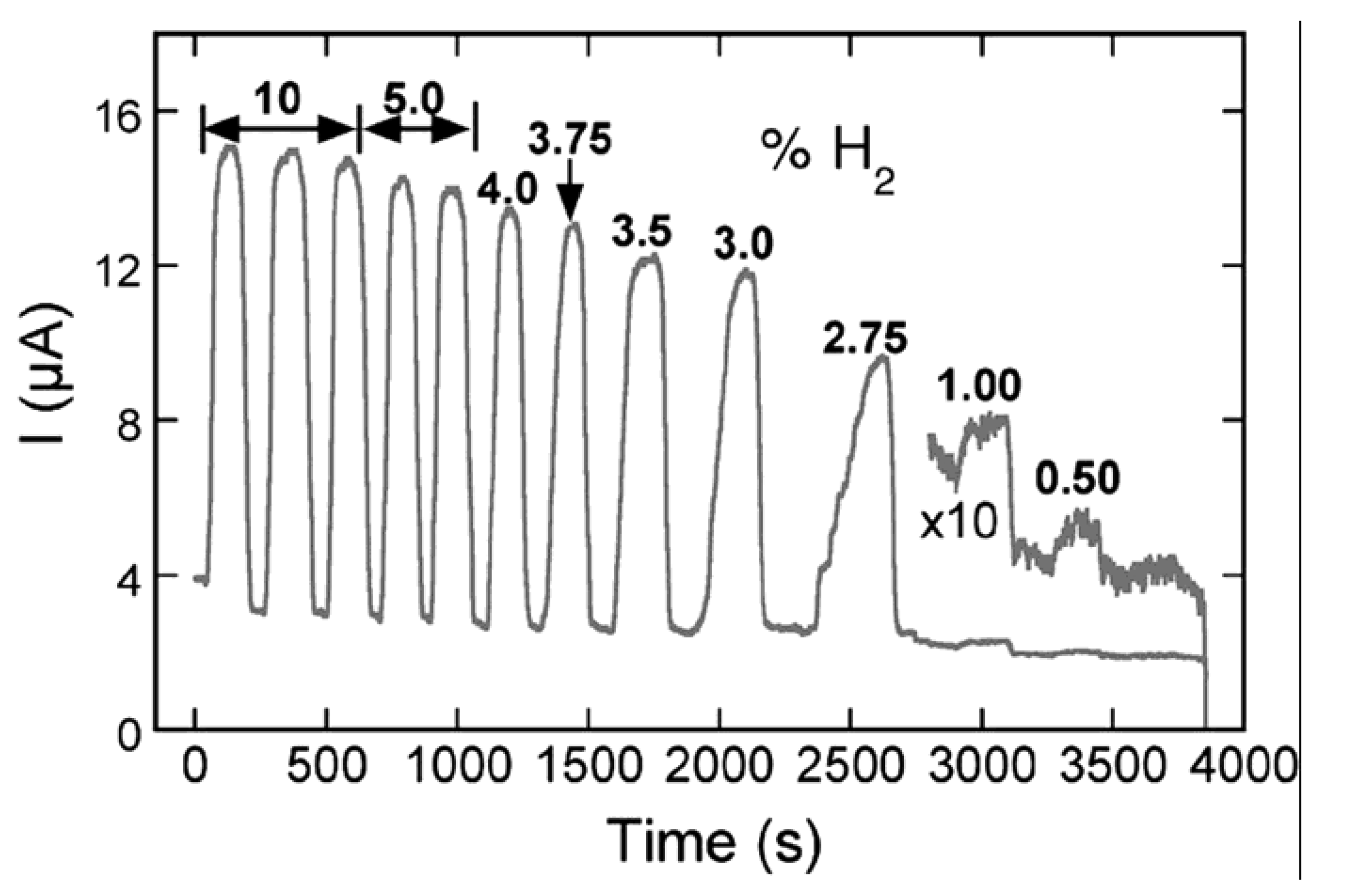
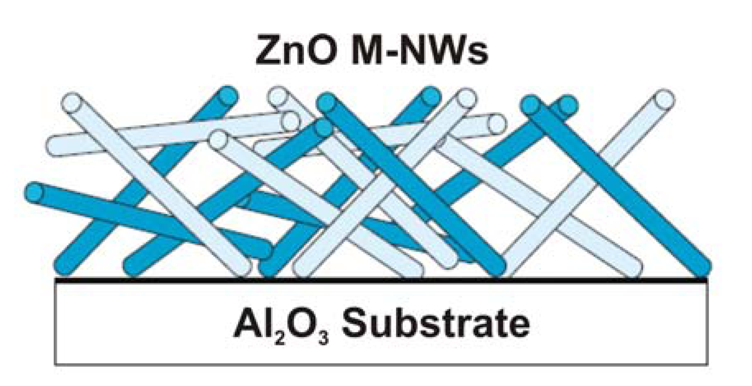
4.1. ZnO Nanowires, Nanorods and Nanotubes

Comparitive studies of ZnO nanowires, rods and tubes in presence and absence of Pt have been reported in detail by Rout et al. [61]. For their experiments, ZnO nanowire arrays have been prepared by electrophoretic deposition in AAM templates with 20 nm pores. In which, the alumina template was dissolved in 0.6 M NaOH to obtain nanowire bundles. To prepare ZnO nanotubes, Zn nanowires produced by nebulized spray pyrolysis were oxidized by heating in air at 450 °C at a rate of 5 °C min−1 for 4 h. The ZnO nanorods were synthesized by two procedures. In the first procedure the nanorods (designated as nanorods-1) were prepared by adding triethanolamine (0.07 mol) to a fine powder of Zn(CH3COO)2 .2H2O and grinding the mixture with NaOH (0.02 mol) for 30 min. The product was washed several times in an ultrasonic bath with distilled water and alcohol, followed by drying in air at 80 °C for 2 h. The second procedure was based on oriented attachment of preformed quasi-spherical ZnO nanoparticles. These nanorods (designated as nanorods-2) were prepared as follows; Zn(CH3COO)2 .2H2O was dissolved in methanol under vigorous stirring at 60 °C and 0.03 M KOH in methanol added drop wise to this solution. The resulting solution was refluxed for 24 h to obtain the product, which was washed with alcohol and dried. Finally, these nanowires, nanorods and nanotubes were dipped in a solution of 0.08 M chloroplatinic acid to obtain a coating of Pt.
From scanning electron microscopy (SEM) and tunneling electron microscopy (TEM) images as shown in Fig. 1, it is learnt that the average diameter of the nanorods-1 and 2 is in the 30-40 nm range with the length in the 600-800 nm range. The diameter of the nanowires is in the 20-30 nm range and 1-2 micron in length. The diameter of the ZnO nanotubes was in the range of 60–100 nm. The sensing characteristics of these nanostructures have been investigated before and after impregnating them with 1% Pt. The nanowires exhibit excellent hydrogen sensing characteristics at relatively low temperatures (less than 150 °C) especially when impregnated with Pt. One type of nanorods shows a satisfactory dependence of sensitivity on the hydrogen concentration, along with short recovery and response times. The nanorods and nanowires impregnated with Pt also show high sensitivity for 1000 ppm of ethanol at or below 150 °C, with short recovery and response times.
Similar report on Pt coated ZnO nanowires by sputtering are shown to selectively detect hydrogen at room temperature [62]. In this report, authors claim that there are no differences in the current-voltage characteristics for measurement in air, N2, or vacuum. The single nanowires operate at extremely low power levels of ∼15-30 μW, which is approximately a factor of 25 lower than multiple ZnO nanowires operated under the same conditions. The addition of the Pt coatings increased the detection sensitivity of the nanowires for 500 ppm H2 in N2 by approximately an order of magnitude, which is about a factor of two improvements over the similar case for multiple nanowires. Pt coated single ZnO nanowires showed relative responses of ∼20% and 50%, respectively, after 10 or 20 min exposure, respectively, to 500 ppm H2 in N2.
In another report, a variety of different metal catalyst coatings (Pt, Pd, Au, Ag, Ti and Ni) deposited on multiple ZnO nanorods have been compared for their effectiveness in enhancing sensitivity for detecting hydrogen at room temperature [63]. During the device designing, contacts to the multiple nanorods were formed using a shadow mask and sputtering of A1/Ti/Au electrodes. The separation of the electrodes was @30 μm. The resulting sensor is shown in Scheme 1, where the Au wires were bonded to the contact pad for current-voltage (I–V) measurements performed at 25 °C in a range of different ambients (N2, O2 or 10-500 ppm H2 in N2). Authors noted that no currents were measured through the discontinuous Au islands and no thin film of ZnO on the sapphire substrate was observed with the growth condition for the nanorods. Therefore, they report that the measured currents are due to transport through the nanorods themselves. In their sensing studies, the Pt-coated nanorods showed a relative response of up to 8% in room temperature resistance upon exposure to a hydrogen concentration in N2 of 500 ppm. This is a factor of two larger than that obtained with Pd and more than an order of magnitude larger than that achieved with the remaining metals. The power levels for these sensors were low, ∼0.4 mW for the responses noted above. Pt coated ZnO nanorods easily detected hydrogen down to 100 ppm, with a relative response of 4% at this concentration after 10 min exposure. The nanorods show a return to their initial conductance upon switching back to a pure-air ambient with time constants of the order of a few minutes at room temperature. This slow response at room temperature is a drawback in some applications, but the sensors do offer low-power operation and ppm detection sensitivity.

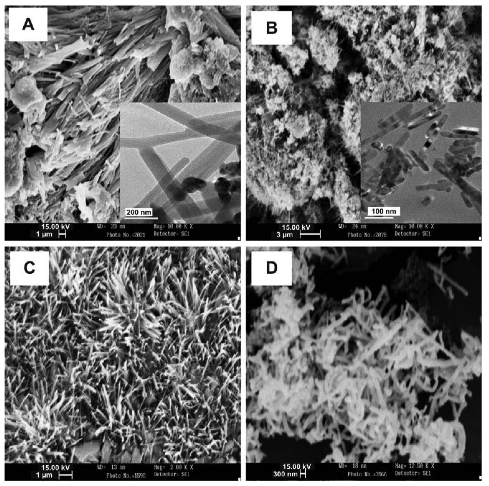
4.2. Beaded Metal Nanowires (Pd, Cd, Mo, Au, Ag, Cu)

Walter et al. reported the preparation of nanowires of different metals by using electrodeposition at step edges present on a graphite surface [64]. For beaded nanowires, nickel, gold and palladium particles were first electrodeposited from aqueous solution of Ni2+, Au2+ or Pd2+, respectively. In the second step, nanowires of molybdenum oxide (MoOx) or palladium were then grown from MoO42− or Pd2+ solutions, respectively. Briefly, the process involves a freshly cleaved graphite surface on which a nucleation pulse was first applied for a few milliseconds at a potential well negative of the reversible potential for metal deposition. After this nucleation pulse, the growth of particles or wires was carried out for durations from a few tens of seconds to a couple of hours using lower overpotentials.
As authors estimated by the SEM measurements, for both particles and wires, diameters were ranged from 50 nm up to 1 mm depending on the particular metals. This “slow-growth” method yielded dispersions of particles ranging in diameter from 50 nm to 5 mm having a relative standard deviation as low as 7%. Using the same method, metal nanowires (Mo and Pd) prepared in the range of diameter from 50 nm up to 1 mm (dispersity of about 10%) with millimeter lengths. Among these various metals beaded nanowires, palladium nanowires have been used as hydrogen sensors. As shown in Fig. 2, the resistance of the sensor decreased in presence of H2. This decrease was related to H2 concentration. After a first series of exposure to hydrogen, this sensor acted as a hydrogen-activated switch; in absence of H2, the resistance became infinite. Under hydrogen, the switch closed and a device resistivity became measurable. These sensors were insensitive to various gases other than H2 (or D2) including Ar, He, N2, water or poisoning gases like O2, CO or CH4. A response time of 75 ms at 5% H2 has been observed.

4.3. Mo and Pd Metal Nanowires

Based on the electronic conductivity behavior of Mo and Pd nanowires, they have been used in analytical applications as sensors. As we discussed earlier, Walter et al. presented similar electrochemical method for synthesizing Mo and Pd metal nanowires with beads ranging in diameter from a few tens of nanometres up to one micrometre, with millimetre lengths [65]. Briefly, these nanowires have been prepared by the electrodeposition of metal at step edges present on a graphite surface. These nanowires have been used to connect metal nanoparticles (Ni, Au, etc.). Finally, by transferring these nanowires in a polymer cast, they fabricated sensors. Using these nanowires, H2 sensors have been constructed and operated by applying a constant voltage of 5 or 10 mV between the silver contacts and measuring the corresponding 1-20 μA current. The resistance of the sensor decreased in the presence of H2. This decrease was related to H2 concentration, with a limit of detection at 0.5% H2 in N2. The response was fast even at room temperature with diminutive power requirements of <100 nw and a chemical resistance to the usual poisoning gases. They have reported also that the performance of these nanowire array-based sensors challenges the existing H2 sensing technologies.

5. Nanowires for Hydrogen Peroxide and Glucose Sensors

Almost all the following studies in this section used noble metal nanowires with enzyme modified electrodes for H2O2 and glucose sensing. In the following sections, we will discuss each sensor's preparation and their applications in detail.

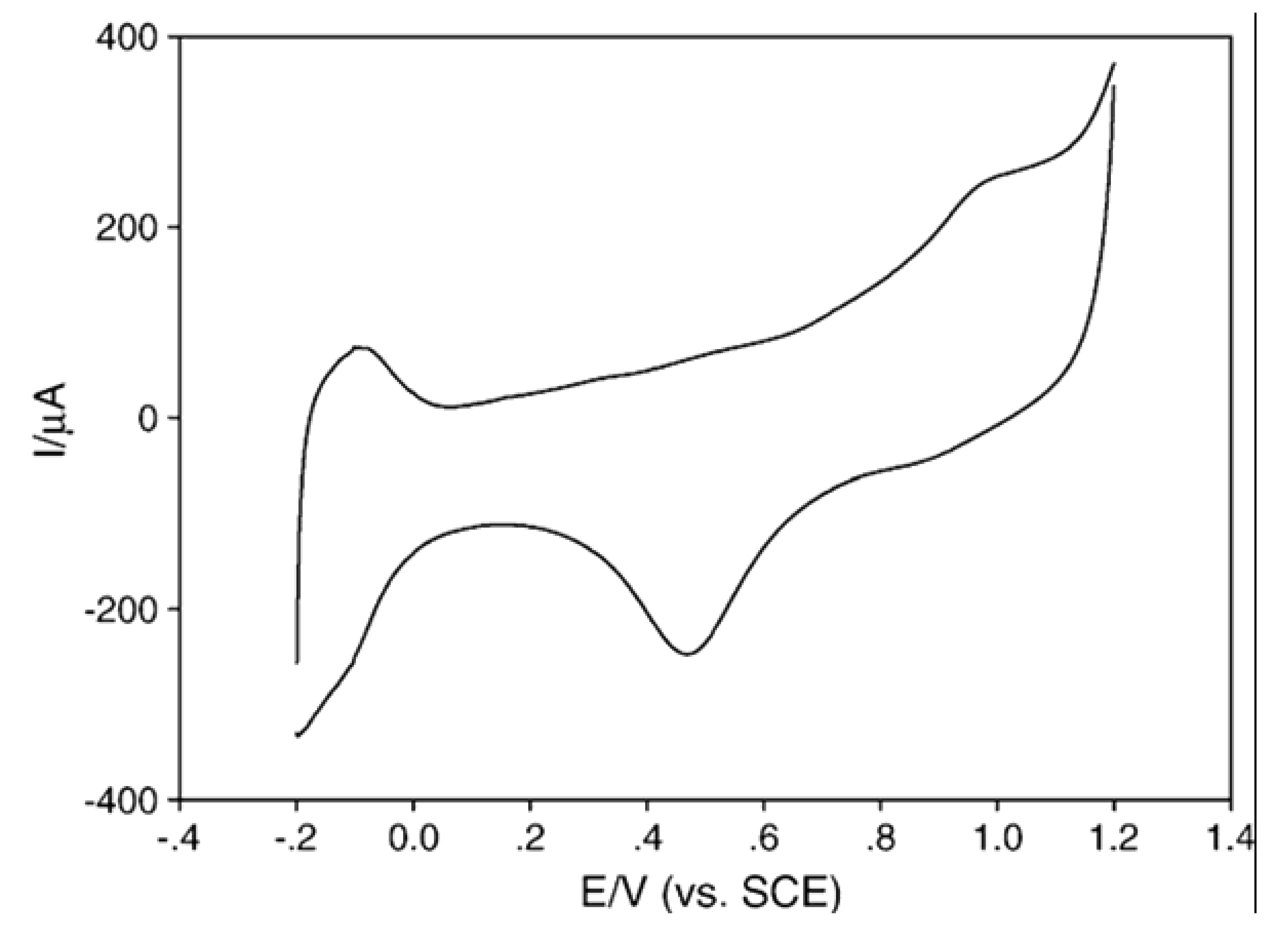
5.1. Gold Nanowires with Chitosan and Glucose Oxidase (GOx)

The Synthesis of Au nanowires in this study has been done by electrodeposition process [66]. In the preparation process prior to the electrodeposition, an ultra thin Au film (30 nm) was first sputtered onto one side of the polycarbonate membrane to make the template conductive. The Au-sputtered membrane, which linked with a brass wire using high purity silver paint, served as a working electrode. Meanwhile, the three electrodes have been immersed into HAuCl4 solution (w/w 1%) containing 0.5 M HClO4, and electrodepositions were performed using chronoamperometry under a constant potential (0.18 V) at room temperature. The whole procedure accompanied continued stirring with a magnetic stirrer. After 15 min of deposition, the polycarbonate (PC) template was dissolved away by immersing in the solution of CHCl3 at 4 °C for 2 h to liberate gold nanowires. The gold nanowire modified electrodes were done by dispersing the prepared gold nanowires within chitosan solutions with the concentration of 2 mg mL−1 by using a short 15 min sonication. After that, 10 μL of the mixture was coated onto the surface of electrode to fabricate gold nanowire modified electrode. Under room temperature, the evaporation of water resulted in a uniform and thin modified film. Further, the prepared gold nanowires modified electrode has been immobilized with enzyme. This enzyme functionalization of gold nanowires were done by immersing the gold nanowires in the GOx solution (10 mg mL−1) overnight at 4 °C in fridge. The functionalized gold nanowires were then dispersed in chitosan solutions under bath sonication for 15 min. The fabrication procedure for enzyme adsorbed gold nanowire modified electrode was similar to the one mentioned above. In brief, the sensor was modified by casting 10 μL of the mixture onto the surface of electrode and dried overnight at 4 °C in fridge to form an infrangible film.
The SEM micrograph of the gold nanowires confirmed the formation of nanowires and it grew well within the pores of PC template and displays a highly regular and uniform pattern with an average diameter of about 250 nm. Estimation of the active surface area of the gold nanowire modified electrode using Fe(CN)64−/3− redox system and Randles–Sevcik equation, showed that the electroactive surface area of the gold nanowire modified electrode is about 2.5 times larger than the bare glassy carbon electrode (GCE). Cyclic voltammetry (CV) studies exhibit the characteristic features expected for metal nanostructure modified electrode as shown in Fig. 3. The well-defined peaks also indicate that the films are highly homogeneous. The electrochemical response of Au nanowire modified electrode toward H2O2 had been examined form its amperometric response toward H2O2. High response current was observed in the range of 0.3 to -0.4 V. The response is higher than in the positive range, indicating the reduction of H2O2 is easier than its oxidation. In this study, the potential of -0.2 V was selected. At such a low applied potential, the background current decreased, the responses of common interference species can be minimized, and the oxygen reduction current can be limited. The sensitivity of the gold nanowire modified electrode is about 30 times higher than conventional gold electrode. Electrochemical performance of the glucose biosensor fabricated by functionalized gold nanowires showed excellent electrocatalytic activity of the modified electrode toward H2O2 which means that the electrode can be served as a new biosensing platform that provides operational access to a great deal of oxidase. Moreover, the good biocompatibility and large specific surface area of gold nanowires made it ideal for the adsorption of enzymes. The amperometric responses of the GOx modified biosensor for successive addition of 0.5 mM glucose at -0.2 V were presented. The resulting glucose biosensor exhibited sensitive response, with a short response time (<8 s), a linear range of 10−5-2×10⁻² M and detection limit of 5×10⁻⁶ M.
Interference from electroactive species, such as ascorbic acid (AA), uric acid (UA) and acetaminophen, which are existing in physiological samples were also studied. The level of endogenous ascorbic and uric acid is about 0.125 and 0.33 mM, respectively, whereas about 0.13 mM acetaminophen has been detected from blood samples. At this level, the glucose biosensor exhibited negligible response to such electroactive interfering species. The authors reported that the relative standard deviation (RSD) values were obtained through three determinations of recovery tests which were low, and it means that the GOx are stably absorbed onto the electrode surface and can be used for practical application. The stability studies show that in the first two weeks, little change of the response current was observed. One month later, there is a slight decrease of the response current, and still 85% of the response can be obtained.

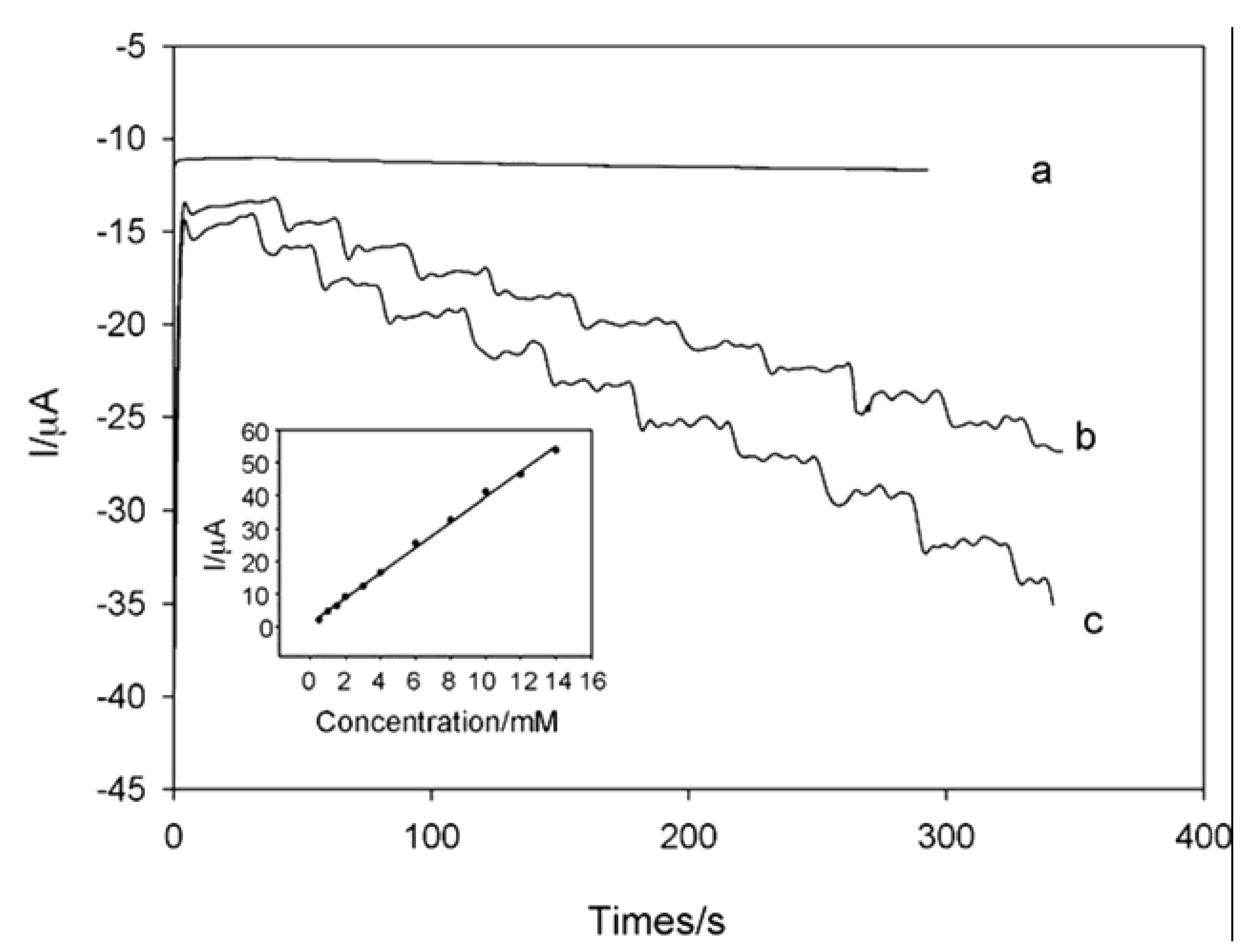
5.2. Platinum Nanowires with CNTs, Chitosan and GOx

The preparation of Pt nanowires were done using a thin gold film (30 nm) sputtered onto one side of the porous anodic aluminum oxide (AAO) template with a nominal pore diameter of 200 nm [67]. Then a copper wire (5 cm) was combined with the porous AAO template sputtered with thin gold film using high purity silver paint. The preparation of AAO template was completed when the silver paint air dried in room temperature. The H2PtCl6 solution of 1% (w/w) containing 1.5 M HClO4 was prepared for the deposition. Then, the potentiostatic electrodeposition with a deposition time of 30 min at the potential of -0.35V was employed. The alumina template with a black layer was washed with double distilled water then immersed into a 8% phosphoric acid at 4 °C for 12 h to liberate the Pt nanowires (PtNW). After the template was dissolved, the resulting nanowires were washed repeatedly using ethanol and double distilled water. The preparation of PtNW-CNT-chitosan film modified electrodes was done by casting 10 μL of PtNW-CNT-chitosan mixture on the surface of GCE. For immobilization of enzymes, the above film modified electrode was immersed into 0.25% glutaric dialdehyde solution for 1 h, after washed with water and dried, 10 μL of GOx solution (20 mg mL−1) was dropped onto the electrode surface and dried at 4 °C.
The authors reported SEM and TEM characterization, which shows that the high-density and well-aligned PtNWs present a comparatively even distribution of diameters of 250 nm with the RSD of 2.3%. The average length of the nanowires is 5μm with the RSD of 7.2%. Films of CNT-chitosan, PtNW-chitosan and PtNW-CNT-chitosan were studied by CV. The CVs suggests that the introduction of CNTs did not affect the electron-transfer process between the PtNWs and the electrode support. In fact, the introduction of CNTs in the biopolymer amplified the peak current of PtNWs by @2 times which revealed the presence of synergistic effects in PtNW-CNT-chitosan film leading to improved redox of PtNWs. The average value of the electroactive surface area for PtNW-CNT-chitosan modified electrode was reported as (0.52±0.3) cm2 (n = 6) compared to (0.38±0.2) cm2 (n=6) for the PtNW-chitosan modified electrode and (0.21±0.2) cm2 (n = 6) for the CNT-chitosan electrode. The detection of H2O2 was studied, which shows an obvious increase of the cathodic current, indicating PtNW-CNT-chitosan film exhibited excellent electrocatalytic activity. The PtNW-CNT-chitosan film modified electrode offered a significant decrease in the overvoltage for the H2O2 and showed to be excellent amperometric sensors for H2O2 at -0.1 V over a wide range of concentrations, and the sensitivity is reported as 260 μA mM−1 cm−2.
As an application example, by linking GOx, an amplified biosensor toward glucose was reported in this same work as shown in Fig. 4. The glucose biosensor exhibits a selective determination of glucose at -0.1 V with a linear response range of 5×10⁻⁶ to 1.5×10⁻² M with a correlation coefficient of 0.997, and response time <10 s. The high sensitivity of the glucose biosensor is up to 30 μA mM−1 cm−2 and the detection limit was 3 μM. The biosensor displayed rapid response and expanded linear response range, and excellent repeatability and stability. The interference test of the glucose biosensor was also carried out at -0.1V in the presence of 0.1 mM AA, 0.1 mM UA, and 1 mM acetaminophen. Compared to the responses of glucose, the current generated due to the interfering species are negligible, indicating high selectivity of the biosensor. In addition authors also report that the choline and ethanol did not cause any observable interference. The recovery of glucose in urine samples was also testified. The results showed that the PtNW-CNT-chitosan/GOx glucose biosensor could be used for the determination of glucose, with satisfactory recoveries of 95.28-105.6%.

5.3. GoldNanowires/MPA/MPE with GOx

The preparation and characterization of gold nanowires in these studies are similar to the section 5.1. The formation of self assembled monolayer (SAM) was accomplished by adsorption of the thiols on the nanostructured gold surface; where the substrates were immersed for 17 h in 2 × 10⁻³ M of 3-mercaptopropionic acid (MPA) or 2-mercaptoethylamine (MPE) using ethanol as a solvent. The samples were then rinsed with ethanol and dried under a nitrogen stream [68]. The terminal carboxylic acid groups of MPA modified gold surfaces were activated by immersion in a pH 3.5 MES buffer solution containing 2 mM l-ethyl-3-(3-dimethylaminopropyl) carbodiimide hydrochloride and 5 mM N-hydroxysuccinimide for 2 h. The surface was rinsed with the buffer solution and immediately placed in a solution of GOx in a phosphate buffer of 0.1 M. Electrodes were incubated for 2 h in 1 mg ml−1 GOx solution. Further, they have reported that the self-assembled cysteamine monolayers were soaked for 2 h in a solution of glutaraldehyde (commercial solution diluted 100 times in phosphate buffer) at room temperature. Again, the resulting monolayers were rinsed with buffer and placed for 2 h in a solution of GOx in phosphate buffer. Enzyme electrodes were rinsed with phosphate buffer and used immediately or stored at 4 °C in buffer solution.
The formation of SAMs on electroless has been qualitatively assessed by measurements of contact angles of water. For bare electroless gold, a contact angle of 75±8 ° was found. This value decreases to 32±3° for gold nanowire/MPE and to less than 10° for gold nanowire/MPA. This modification of the contact angles is therefore a useful proof of the presence of hydrophilic at the surface of electroless gold. In the electrochemical characterization, the values of the peak current for nanostructured and non-nanostructured systems show that, ratio between the peak current in the presence and in the absence of the nanostructured film ranging from 9.79 up to 15.23, which indicates an increase of the electrochemical response using the nanowired system. Further, the authors conducted experiments for chemical and morphological characterization, which have been done by X-ray Photoelectron Spectroscopy (XPS) and AFM, which revealed the presence of the gold nanowires, oriented mostly perpendicularly to the surface, also the values of average roughness increase from 45.4 to 65.6 nm after the enzyme immobilization. Finally, they reported about the electrochemical detection of glucose, where the high response could be due to the higher roughness of the nanostructured surface compared to a flat gold electrode and to the tubular nature of the electrode, both leading to an increased surface area of the electrode for the same geometric area.

6. Nanowires for Cholesterol Sensor

Gold nanowires with cholesterol oxidase (COx) and cholesterol esterase (CE) possess excellent properties for the cholesterol detection. In the following sections, we will discuss two different sensor's preparation and studies in detail.

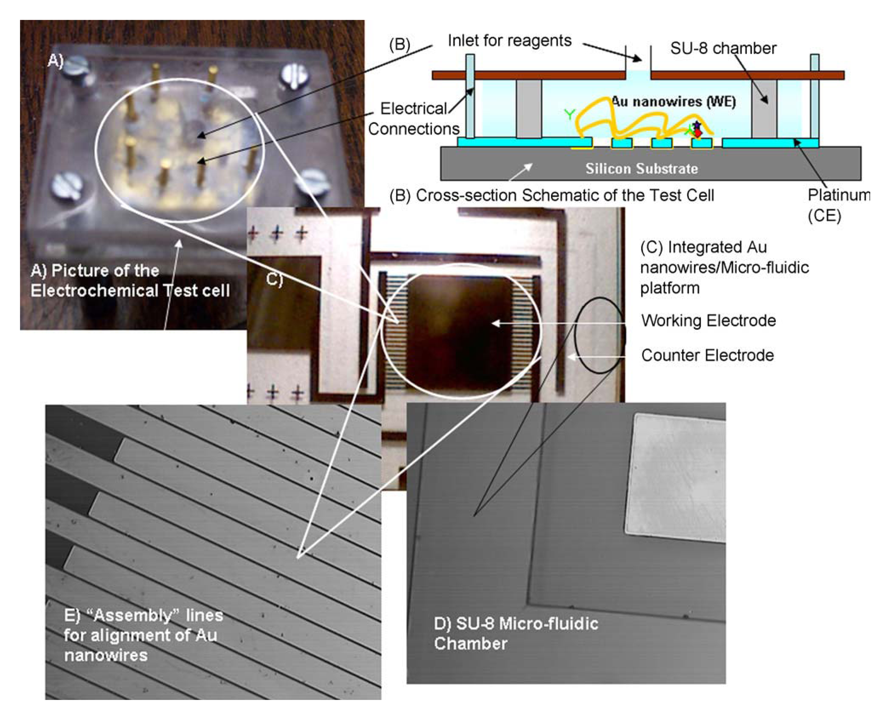
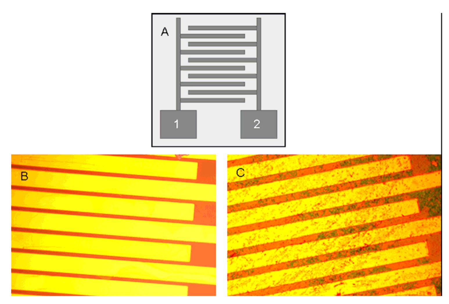
6.1. MEMS Micro-Fluidic Platform Modified with Gold Nanowires

The principle of this biosensor is based on the amperometric detection of H2O2, which is generated during the course of the enzymatic oxidation of cholesterol by dissolved oxygen. Square wave voltammogram technique was used to study the electrochemical behavior. Aravamudhan et al. [69] fabricated gold nanowires for the preparation of nanowire micro-fluidic platform by electroplating inside the 200 nm pores of commercial alumina template. The aluminium layer was evaporated on one side of the alumina template to act as an electrode for electroplating. The electroplating was performed at a current density of 2.5 to 4 mA cm−2 and 55 °C. Platinum mesh acted as anode and alumina template (with one side coated with aluminium) acted as cathode. After electroplating for about 1 h, the sample was thoroughly rinsed in deionized water. Then, to liberate the gold nanowires, alumina template with aluminium on one side was dissolved in warm 45% KOH with periodic agitation. This resulted in release of Au nanowires in solution. Then, the gold nanowires were collected from KOH by centrifugation at 7000-9000 RPM. The supernatant was decanted and replaced with clean methanol. The nanowires were sonicated for 1 min and this protocol of collection-solvent addition-sonication was repeated three times to completely wash the nanowires.
The micro-fluidic platform (Fig. 5A and B) was fabricated in a (1 0 0) silicon substrate (2.5 × 2.5 mm) using photolithography, subsequent e-beam evaporation and lift-off of Ti/Pt electrodes. Ti acts as adhesion layer for Pt. Two sets of Pt electrodes namely (1) “assembly lines” for nanowire alignment and (2) counter electrode were fabricated on the substrate. This was followed by fabrication of 60 μm tall micro-fluidic chamber by hard baked at 180 °C for 3 min to prevent any out-gassing or contamination. The integration of Au nanowires into the micro-fluidic platform (Fig. 5D) was achieved utilizing dielectrophoresis/electric-field-assisted technique. Dilute suspensions (200 μL, approximately 107 wires mL−1) of the nanowires were dispensed on to the “assembly” lines/chamber; alternating voltage ranging from 10 to 50 Vrms was applied for about 15 to 45 seconds between the lines. This resulted in movement of nanowires towards regions of highest field intensity, and subsequent alignment of the nanowires bridging the “assembly” lines.
Before using the sensor, the working electrode was modified by surface functionalization. The functionalization process involves the cleaning of gold nanowires in piranha solution (1:3 H2O2 and H2SO4) and then, rinsed in excess deionized water. Then, the gold nanowires were activated with 2% (w/w) thioctic acid in absolute ethanol with shaking. The nanowires were then rinsed in ethanol twice and dried. Then, the gold nanowires were immobilized using carboxyl-terminated chemistry. Finally, 250 μg mL−1 of streptavidin in phosphate buffer was specifically immobilized on the gold surface and incubated at 4 °C overnight. Twenty five microlitres of 0.1 M COx was immobilized on the integrated gold nanowire/micro fluidic platform. Then, 25 μL of 0.1 M CE in 0.1 M PBS and 2 μL of Triton X-100 was immobilized on the sensor surface. Finally, the gold nanowire/micro-fluidic platform was incubated for 24 h at 4 °C and thoroughly rinsed in phosphate buffer before measurements.
The SEM analysis clearly showed immobilization of biotin-streptavidin linkage on the gold nanowires. AFM image shows globules of COx/CE molecules on the electrode surface. The size of the globules is much larger than that of one molecule because of non-spherical shape of the globules after adsorption. FTIR spectra, further confirmed the functionalization of COx/CE on gold nanowires. The calibration plot for determination of total cholesterol was created by taking the peak current values of each curve and plotting this current for each cholesterol level. These results showed that the sensor is more efficient. Further, authors reported stability analysis, where twenty runs at 4 mM cholesterol concentration yielded a very stable response that changed an indiscernible amount. The storage stability was tested by measuring the current response for the modified electrode, which was stored dry at 4 °C at different time intervals. In all, the storage stability studies prove the suitability of such modified gold nanowires as disposable sensors. Finally, the interferences studies were done by two methods namely (1) at normal level of interferences and (2) at higher level of interferences were performed. Normal level of interferences such as AA (2 μM), UA (10 μM), and glucose (20 μM) found usually in blood serum had no significant effect on the electrochemical current response. The response from higher level of interferences and the square wave voltammogram response for two cholesterol levels (3 and 5 mM) with 50 μM of urea, 100 μM of glucose and 4 μM of AA were conducted. Interestingly, the current response was within the error range of ± 4% implying no significant contribution. The modified gold nanowire sensor showed a stable calibration line and a quasi-linear relationship between cholesterol level and current response in the range of 1-6 mM (in steps of 1 mM over the baseline blood serum). The sensitivity of the modified electrode was found to be about 69 nA mM−1 with good storage and interference stability.

6.2. Gold Nanowires with COx and CE

This work [70] is almost similar to the above mentioned report in section 6.1. The device designing and the gold nanowires preparation were done by using micro-fluidic platform for sensitive and selective estimation of targeted species, such as cholesterol in blood. The aligned gold nanowires were modified with specific enzymes COx and CE, using covalent chemistry to act as the working electrode. Fig. 6 illustrates the alignment of Au nanowires on the Pt lines, achieved using dielectrophoresis (DEP) technique. The biosensor showed a linear relationship between cholesterol level (10-60 μM) and current response, with a sensitivity of 0.85 nA μM−1, which are different from the above mentioned result. Further, studies performed with higher level of interfering species usually found in blood showed a stable and selective electrochemical response.

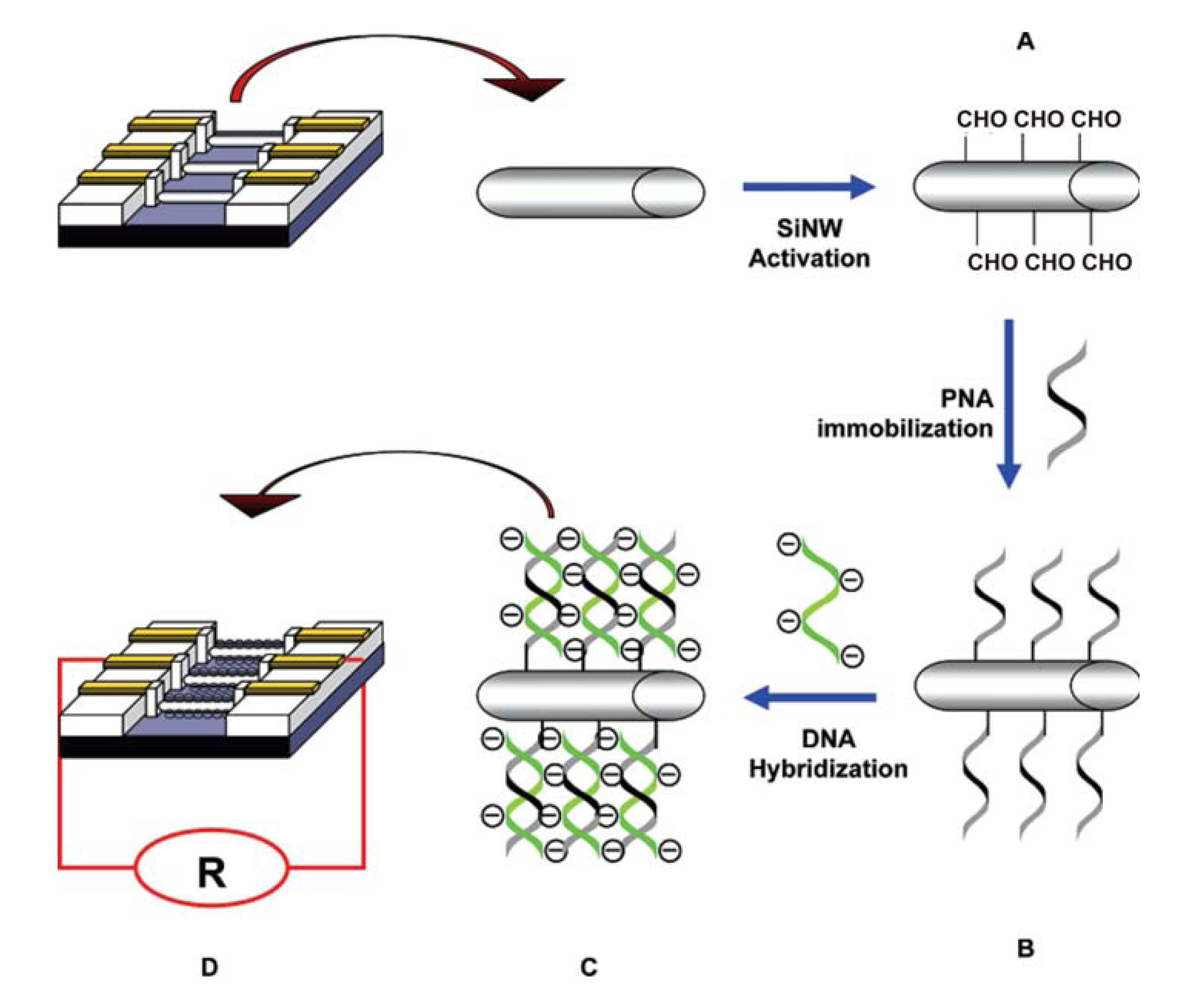
7. Nanowires for DNA Sensor

Silicon nanowires and DNA modified gold nanowires have been used for the DNA sensors. In one of the literature [71], arrays of highly ordered n-type silicon nanowires (SiNW) are fabricated using complementary metal-oxide semiconductor compatible technology as shown in Scheme 2. Peptide nucleic acid (PNA) capture probe-functionalized SiNW arrays show a concentration dependent resistance change upon hybridization to complementary target DNA that is linear over a large dynamic range with a detection limit of 10 fM. As with other SiNW biosensing devices, the sensing mechanism can be understood in terms of the change in charge density at the SiNW surface after hybridization, the so-called “field effect”. The SiNW array biosensor discriminates satisfactorily against mismatched target DNA. It is also able to monitor directly the DNA hybridization event in situ and in real time. The SiNW array biosensor described here is ultrasensitive, non-radioactive, and more importantly, label-free, and is of particular importance to the development of gene expression profiling tools and point-of-care applications.
Similarly, arrayed gold nanowires were used for electrochemical DNA detection [72]. Pilot studies testing the use of these template structures with an electrocatalytic reporter system revealed that very low detection thresholds for target DNA sequences only can be obtained. One factor contributing to the heightened sensitivity is the high signal-to-noise ratio achieved with the large electrocatalytic signals observed at DNA-modified nanowires. Here, the authors explained the improved sensitivity with evidence illustrating that electrocatalysis at DNA-modified nanostructures generates amplified signals that are significantly larger than those observed at bulk gold surfaces. The results presented strongly suggest that the three dimensional architectures of the nanowires facilitate the electrocatalytic reaction because of enhanced diffusion occurring around these structures. Effects unique to the nanoscale are shown to underlie the utility of nanowires for DNA biosensing.

8. Nanowires for Other Chemical Sensors and Biosensors

Other than the above discussed sensors, in the literature, other types of nanowire modified electrodes for different types of sensors have been reported. In the following sections, we will briefly discuss these sensors.

8.1. La(OH)3 Nanowires Modified Carbon Paste Electrode (CPE) for Inosine Sensor

La(OH)3 nanowires (LNWs) with an average diameter of 15-20 nm were prepared by hydro-thermal method [73], and were directly used without further treatment. The LNW/CPE was prepared by hand-mixing 0.98 g graphite power, 0.02 g LNWs and 0.2 mL paraffin oil. The CNT modified carbon paste electrode (CNT/CPE) was also prepared in a similar manner by mixing 0.98 g graphite power, 0.02 g CNT and 0.2 mL paraffin oil. The surfaces of all the modified and unmodified CPEs were carefully smoothed on weighing paper and rinsed with water prior to each measurement. Unmodified CPE was prepared by mixing 1.0 g graphite powers and 0.2 mL paraffin oil adequately in agate mortar. A portion of the resulting paste was then packed firmly into the electrode cavity (2.6 mm diameter) of a PTFE sleeve. Electrical contact was established via a copper wire. For electrocatalysis experiments, a 10 mL of 0.1 mol L−1 phosphate buffer (pH 6.7) containing appropriate inosine, 6.0×10⁻⁶ mol L−1 Cu(II) ion and 6.0×10⁻⁶ mol L−1 K2S2O8 solution was mixed. After 35 min, the obtained solution was transferred into a voltammetric cell for various studies.
The voltammetric behaviors of inosine at LNW modified CPE in the presence of Cu(II) ion and K2S2O8 were investigated. The oxidation peak at 0.20 V was attributed to inosine oxidation in the formed inosine-Cu(II) complex, while the reduction peak at -0.20 V was attributed to Cu(II) ion reduction in the complex. The electrochemical oxidation potential of inosine was reduced, and the analytical sensitivity and selectivity was improved. From these results, a novel sensing system for monitoring inosine was proposed by the authors. The oxidation peak current at 0.20 V was rectilinear with inosine concentration in the range of 4.0×10⁻⁹ to 2.0×10⁻⁸ mol L−1, with a detection limit of 8.3×10⁻¹⁰ mol L−1. The proposed system was also applied to inosine determination in both pharmaceutical preparations and human serum.

8.2. Gold Nanowires with Glycoconjugate (Antibody) for Bacterial Detection and Octadecanethiol Sensor

Two types of sensors are explained in this section which is composed of gold nanowires. Among these two, one sensor is made of gold nanowires with glycoconjugate (antibody) which is used for bacterial detection [74]. The authors report that, they developed a rapid method for UTI detection in very low bacteria concentration, applying current knowledge of nano technology. Experiments have been designed for the development of biosensors using nanowired structures coated with elements such as gold that have affinity for biomolecules. The basic principle for the detection procedure of the infection is partly based on the enzyme-linked immunosorbent assay system. Anti-E. coli antibody-bound gold nanowire arrays prepared on anodized porous alumina template is used for the primary step followed by binding of the bacteria containing specimen. An alkaline phosphatase-conjugated second antibody is then added to the system and the resultant binding determined by both electrochemical and optical measurements. Various kinds of gold nanowires array templates were used in order to determine the one with the best affinity for antibody binding. In addition, an efficient method for enhanced antibody binding has been developed with the covalent immobilization of an organic linker dithiobissuccinimidylundecanoate on the gold nanowires array surface. Studies have also been conducted to optimize the antibody-binding conditions to the linker-attached gold nanowires array surfaces for their ability to detect bacteria in clinical concentrations.
Another application of gold nanowires is reported by Liu et al. for octadecanethiol sensor [75]. They reported the fabrication of single nanoporous gold nanowires and demonstrate that adsorption of an alkanethiol can be monitored in real time. Single nanowire devices were fabricated by in situetching of Au 0.18 Ag 0.82 alloy nanowires in dilute nitric acid. The evolution of the porous structure was characterized by monitoring the resistance change and comparing to cross-sectional images. The feature size of about 10 nm is less than the mean free path for electrons in bulk gold, and hence the resistance is dominated by surface scattering. Adsorption of a monolayer of octadecanethiol onto the nanoporous gold nanowire results in a resistance change of about 3%. The sensitivity factor of 1.0 × 10⁻¹⁶ cm2 is comparable to values reported for adsorption at ultrathin films.

8.3. Silica Nanowires for the Detection of Cancer Biomarkers Exemplified by Interleukin-10 and Osteopontin

Ramgir et al. reported real-time voltammetric detection of potential lung cancer biomarkers, namely, interleukin-10 (IL-10) and osteopontin (OPN), using localized silica nanowires as templates, through an electrochemical alkaline phosphatase (AP) based assay [76]. The high surface to volume ratio associated with nanowires enhances the loading of a specific capture antibody toward a particular cancer antigen. An AP enzyme attached to the cancer antigens (IL-10 and OPN) via detector antibodies hydolyses (dephosphorylates) the p-nitrophenyl phosphate substrate to a yellow, water-soluble product, p-nitrophenol (pNP). This was detected in a small test volume of 3 μL, using a microelectrode cell fabricated in Au. The electro-oxidation of pNP occurs between 0.85 and 0.9 V with anodic peak current showing linear dependence with the capture antibody and antigen concentrations, respectively. The detection of IL-10 down to 1 fg mL−1 in ideal pure solution and 1 pg mL−1 in clinically relevant samples was achieved reproducibly. Moreover, both the concentration of the capture antibody and the cancer antigen were found to have a strong influence on the anodic peak current, as demonstrated considering specific example of OPN.

8.4. Silver Mesowires for Amine Vapor Sensor

Silver mesowires with diameters ranging from 150 to 950 nm and lengths of 100 μm or more were prepared by electrochemical step edge decoration [77]. Upon exposure to ammonia (NH3) vapor, ensembles of these mesowires showed a resistance increase, ΔR/Ro, that was large (up to 10,000%), fast (<5 s), and reversible. The vapor of liquid amines, including pyridine and trimethylamine, produced a similar but slower (1 min) response. Hydrogen sulfide caused a large, irreversible resistance increase and carbon monoxide, dioxygen, hydrocarbons, argon, and water, caused no change in resistance for exposures of up to 10 seconds. Exposure to NH3 also induced unexpectedly large resistance increases for mesowires of copper and platinum but metal films showed a maximum ΔR/Ro of < 5%, just as reported previously. Atomic force microscopy analysis of individual silver wires suggests that the increased resistance induced by NH3 exposure was concentrated at a minority (<10%) of the interparticle boundaries present along the axes of these wires.

9. Conclusions

The unique properties of nanowires such as mechanical stability, light weight, enhancement in the current, reduction in potential are very helpful for the development of efficient electrochemical sensors and biosensors. Functional nanowire arrays constitute one of the most fascinating current issues in the nanotechnology field. Given that most of the applications described above are concerned with pushing the limits of how few molecules can be detected in a given volume of solution. Nanowire sensors are inherently useful so long as the entire platforms are designed in such a way that the entire sample volume can be interrogated by the sensor. Also, their electrical, thermal, magnetic and optical properties are excellent. However, the real value of sensors lies in their detection limit range, sensitivity, etc., and all these are enhanced by the nanowire modified electrodes in the sensors. These overall properties provide additional benefits, which enable development of sensors made of multifunctional, structural materials. In a few more years nanowire sensors will become prominent among researchers and in market. They will be small in size and high in sensitivity.

Acknowledgments

National Taipei University of Technology assisted in meeting the publication costs of this article.

References

  1. Wilson, G.S.; Gifford, R. Biosensors for real-time in vivo measurements. Biosens. Bioelectron. 2005, 20, 2388–2403. [Google Scholar] [CrossRef]
  2. Sakaguchi, T.; Morioka, Y.; Yamasaki, M.; Iwanaga, J.; Beppu, K.; Maeda, H.; Morita, Y.; Tamiya, E. Rapid and onsite BOD sensing system using luminous bacterial cells-immobilized chip. Biosens. Bioelectron. 2007, 22, 1345–1350. [Google Scholar] [CrossRef]
  3. Chen, S.M.; Chzo, W.Y. Simultaneous voltammetric detection of dopamine and ascorbic acid using didodecyldimethylammonium bromide (DDAB) film-modified electrodes. J. Electroanal. Chem. 2006, 587, 226–234. [Google Scholar] [CrossRef]
  4. Vasantha, V.S.; Chen, S.M. Electrocatalysis and simultaneous detection of dopamine and ascorbic acid using poly(3,4-ethylenedioxy)thiophene film modified electrodes. J. Electroanal. Chem. 2006, 592, 77–87. [Google Scholar] [CrossRef]
  5. Simoyi, M.F.; Falkenstein, E.; Dyke, K.V.; Blemings, K.P.; Klandorf, H. Allantoin the oxidation product of uric acid is present in chicken and turkey plasma. Comparative Biochemistry and Physiology Part B 2003, 135, 325–335. [Google Scholar] [CrossRef]
  6. Balasubramanian, K.; Burghard, M. Biosensors based on carbon nanotubes. Anal. Bioanal. Chem. 2006, 385, 452–468. [Google Scholar] [CrossRef]
  7. Zhang, S.; Wang, N.; Niu, Y.; Sun, C. Immobilization of glucose oxidase on gold nanoparticles modified Au electrode for the construction of biosensor. Sens. Act. B. 2005, 109, 367–374. [Google Scholar] [CrossRef]
  8. Wang, J.; Musameh, M.; Lin, Y. Solubilization of carbon nanotubes by nafion toward the preparation of amperometric biosensors. J. Am. Chem. Soc. 2003, 125, 2408–2409. [Google Scholar] [CrossRef]
  9. Yogeswaran, U.; Thiagarajan, S.; Chen, S.M. Nanocomposite of functionalized multiwall carbon nanotubes with nafion, nano platinum, and nano gold biosensing film for simultaneous determination of ascorbic acid, epinephrine, and uric acid. Anal. Biochem. 2007, 365, 122–131. [Google Scholar] [CrossRef]
  10. Yogeswaran, U.; Chen, S.M. Separation and concentration effect of f-MWCNTs on electrocatalytic responses of ascorbic acid, dopamine and uric acid at f-MWCNTs incorporated with poly (neutral red) composite films. Electrochim. Acta. 2007, 52, 5985–5996. [Google Scholar] [CrossRef]
  11. Hubalek, J.; Hradecky, J.; Adam, V.; Krystofova, O.; Huska, D.; Masarik, M.; Trnkova, L.; Horna, A.; Klosova, K.; Adamek, M.; Zehnalek, J.; Kizek, R. Spectrometric and voltammetric analysis of urease – nickel nanoelectrode as an electrochemical sensor. Sensors 2007, 7, 1238–1255. [Google Scholar]
  12. Yogeswaran, U.; Thiagarajan, S.; Chen, S.M. Pinecone shape hydroxypropyl-β-cyclodextrin on a film of multi-walled carbon nanotubes coated with gold particles for the simultaneous determination of tyrosine, guanine, adenine and thymine. Carbon 2007, 45, 2783–2796. [Google Scholar] [CrossRef]
  13. Yogeswaran, U.; Chen, S.M. Electrocatalytic properties of electrodes which are functionalized with composite films of f-MWCNTs incorporated with poly(neutral red). J. Electrochem. Soc. 2007, 154, E178–E186. [Google Scholar]
  14. Kim, I.J.; Han, S.D.; Han, C.H.; Gwak, J.; Lee, H.D.; Wang, J.S. Micro semiconductor CO sensors based on indium-doped tin dioxide nanocrystalline powders. Sensors 2006, 6, 526–535. [Google Scholar]
  15. Lyons, M.E.G.; Keeley, G.P. The redox behaviour of randomly dispersed single walled carbon nanotubes both in the absence and in the presence of adsorbed glucose oxidase. Sensors 2006, 6, 1791–1826. [Google Scholar]
  16. Liang, W.; Zhuobin, Y. Direct electrochemistry of glucose oxidase at a gold electrode modified with single-wall carbon nanotubes. Sensors 2003, 3, 544–554. [Google Scholar]
  17. Hernandez-Velez, M. Nanowires and 1D arrays fabrication: An overview. Thin Solid Films. 2006, 495, 51–63. [Google Scholar] [CrossRef]
  18. Yogeswaran, U.; Chen, S.M. Multi-walled carbon nanotubes with poly(methylene blue) composite film for the enhancement and separation of electroanalytical responses of catecholamine and ascorbic acid. Sens. Act. B 2008, 128. in press. [Google Scholar] [CrossRef]
  19. Shie, J.W.; Yogeswaran, U.; Chen, S.M. Electroanalytical properties of cytochrome c by direct electrochemistry on multi-walled carbon nanotubes incorporated with DNA biocomposite film. Talanta 2008, 74, 1659–1669. [Google Scholar]
  20. Li, S.; He, P.; Dong, J.; Guo, Z.; Dai, L. DNA-directed self-assembling of carbon nanotubes. J. Am. Chem. Soc. 2005, 127, 14–15. [Google Scholar] [CrossRef]
  21. Vaseashta, A.; Dimova-Malinovska, D. Nanostructured and nanoscale devices, sensors and detectors. Sci. Tech. Adv. Mat. 2005, 6, 312–318. [Google Scholar]
  22. Zhang, X.L.; Wang, J.X.; Wang, Z.; Wang, S.C. Improvement of amperometric sensor used for determination of nitrate with polypyrrole nanowires modified electrode. Sensors 2005, 5, 580–593. [Google Scholar]
  23. Qian, L.; Yang, X. Composite film of carbon nanotubes and chitosan for preparation of amperometric hydrogen peroxide biosensor. Talanta 2006, 68, 721–727. [Google Scholar] [CrossRef]
  24. Wang, J.; Chen, G.; Chatrathi, M.P.; Musameh, M. Capillary electrophoresis microchip with a carbon nanotube-modified electrochemical detector. Anal. Chem. 2004, 76, 298–302. [Google Scholar] [CrossRef]
  25. Curreli, M.; Li, C.; Sun, Y.; Lei, B.; Gundersen, M.A.; Thompson, M.E.; Zhou, C. Selective functionalization of In2O3 nanowire mat devices for biosensing applications. J. Am. Chem. Soc. 2005, 127, 6922–6923. [Google Scholar] [CrossRef]
  26. Roberts, M.A.; Kelley, S.O. Ultrasensitive detection of enzymatic activity with nanowires electrodes. J. Am. Chem. Soc. 2007, 129, 11356–11357. [Google Scholar] [CrossRef]
  27. Shi, L.; Yu, C.; Zhou, J. Thermal characterization and sensor applications of one-dimensional nanostructures employing microelectromechanical systems. J. Phys. Chem. B. 2005, 109, 22102–22111. [Google Scholar] [CrossRef]
  28. Laocharoensuk, R.; Bulbarello, A.; Hocevar, S.B.; Mannino, S.; Ogorevc, B.; Wang, J. On-demand protection of electrochemical sensors based on adaptive nanowires. J. Am. Chem. Soc. 2007, 129, 7774–7775. [Google Scholar] [CrossRef]
  29. Lee, E.P.; Peng, Z.; Cate, D.M.; Yang, H.; Campbell, C.T.; Xia, Y. Growing Pt nanowires as a densely packed array on metal gauze. J. Am. Chem. Soc. 2007, 129, 10634–10635. [Google Scholar] [CrossRef]
  30. Zhu, N.; Chang, Z.; He, P.; Fang, Y. Electrochemically fabricated polyaniline nanowires-modified electrode for voltammetric detection of DNA hybridization. Electrochim. Acta. 2006, 51, 3758–3762. [Google Scholar] [CrossRef]
  31. Tian, Y.; Wang, J.; Wang, Z.; Wang, S. Electroreduction of nitrite at an electrode modified with polypyrrole nanowires. Synthetic Metals. 2004, 143, 309–313. [Google Scholar] [CrossRef]
  32. Hultgren, A.; Tanase, M.; Felton, E.J.; Bhadriraju, K.; Salem, A.K.; Chen, C.S.; Reich, D.H. Optimization of yield in magnetic cell separations using nickel nanowires of different lengths. Biotechnol. Prog. 2005, 21, 509–515. [Google Scholar] [CrossRef]
  33. Wanekaya, A.K.; Chen, W.; Myung, N.V.; Mulchandani, A. Nanowire-based electrochemical biosensors. Electroanalysis. 2006, 18, 533–550. [Google Scholar] [CrossRef]
  34. Müller, T.; Heining, K.H.; Schmidt, B. Formation of Ge nanowires in oxidized silicon V-grooves by ion beam synthesis. Nucl. Instrum. Methods Phys. Res. 2001, 175, 468–473. [Google Scholar]
  35. Sun, Y.; Khang, D.Y.; Hua, F.; Hurley, K.; Nuzzo, R.G.; Rogers, J.A. Photolithographic route to the fabrication of micro/nanowires of III-V semiconductors. Adv. Funct. Mater. 2005, 15, 30–40. [Google Scholar] [CrossRef]
  36. Cheng, F.L.; Zhang, M.L.; Wang, H. Fabrication of polypyrrole nanowire and nanotube arrays. Sensors 2005, 5, 245–249. [Google Scholar]
  37. Penumetcha, S.S.; Kona, R.; Hardin, J.L.; Molder, A.L.; Steinle, E.D. Monitoring transport across modified nanoporous alumina membranes. Sensors 2007, 7, 2942–2952. [Google Scholar]
  38. Martin, C.R. Membrane-based synthesis of nanomaterials. Chem. Mater. 1996, 8, 1739–1746. [Google Scholar] [CrossRef]
  39. Müller, F.; Birner, A.; Schilling, J.; Li, A.P.; Nielsch, K.; Gösele, U.; Lehmann, V. High aspect ratio microstructures based on anisotropic porous materials. Microsyst. Technol. 2002, 8, 7–9. [Google Scholar] [CrossRef]
  40. Choi, J.; Nielsch, K.; Reiche, M.; Wehrspohn, R.B.; Gösele, U. Fabrication of monodomain alumina pore arrays with an interpore distance smaller than the lattice constant of the imprint stamp. J. Vac. Sci. Technol. B. 2003, 21, 763–766. [Google Scholar] [CrossRef]
  41. Masuda, H.; Abe, A.; Nakao, M.; Yokoo, A.; Tamamura, T.; Nishio, K. Ordered mosaic nanocomposites in anodic porous alumina. Adv. Mater. 2003, 15, 161–164. [Google Scholar] [CrossRef]
  42. Masuda, H.; Ohya, M.; Asoh, H.; Nishio, K. Photonic band gap in naturally occurring ordered anodic porous alumina. Jpn. J. Appl. Phys. 2001, 40, L1217–L1219. [Google Scholar]
  43. Bae, E.J.; Choi, W.B.; Jeong, K.S.; Chu, J.U.; Park, G.S.; Song, S.; Yoo, I.K. Selective growth of carbon nanotubes on pre-patterned porous anodic aluminum oxide. Adv. Mater. 2002, 14, 277–279. [Google Scholar] [CrossRef]
  44. Martín, A.; Martínez, F.; Calvo, J.I.; Prádanos, P.; Palacios, L.; Hernández, A. Protein adsorption onto an inorganic microfiltration membrane: Solute-solid interactions and surface coverage. J. Membr. Sci. 2002, 207, 199–207. [Google Scholar] [CrossRef]
  45. Dickey, E.C.; Varghese, O.K.; Ong, K.G.; Gong, D.; Paulose, M.; Grimes, C.A. Room temperature ammonia and humidity sensing using highly ordered nanoporous alumina films. Sensors 2002, 2, 91–110. [Google Scholar]
  46. Asoh, H.; Ono, S.; Hirose, T.; Nakao, M.; Masuda, H. Growth of anodic porous alumina with square cells. Electrochim. Acta. 2003, 48, 3171–3174. [Google Scholar] [CrossRef]
  47. Choi, J.; Wehrspohn, R.; Gösele, U. Moiré pattern formation on porous alumina arrays using nanoimprint lithography. Adv. Mater. 2003, 15, 1531–1534. [Google Scholar] [CrossRef]
  48. Asoh, H.; Matsuo, M.; Yoshihama, M.; Ono, S. Transfer of nanoporous pattern of anodic porous alumina into Si substrate. Appl. Phys. Lett. 2003, 83, 4408–4410. [Google Scholar] [CrossRef]
  49. Hoyer, P. Formation of a titanium dioxide nanotube array. Langmuir 1996, 12, 1411–1413. [Google Scholar] [CrossRef]
  50. Sander, M.S.; Coté, M.J.; Gu, W.; Kile, B.M.; Tripp, C.P. Template-assisted fabrication of dense, aligned arrays of titania nanotubes with well-controlled dimensions on substrates. Adv. Mater. 2004, 16, 2052–2057. [Google Scholar] [CrossRef]
  51. Zhang, R.; Tejedor, M.I.; Anderson, M.A.; Paulose, M.; Grimes, C.A. Ethylene detection using nanoporous PtTiO2 coatings applied to magnetoelastic thick films. Sensors 2002, 2, 331–338. [Google Scholar]
  52. Varghese, O.K.; Paulose, M.; Grimes, C.A.; Dickey, E.C. Crystallization and high-temperature structural stability of titanium oxide nanotube arrays. J. Mater. Res. 2003, 18, 156–165. [Google Scholar]
  53. Sarkar, J.; Khan, G.G.; Basumalick, A. Nanowires: properties, applications and synthesis via porous anodic aluminium oxide template. Bull. Mater. Sci. 2007, 30, 271–290. [Google Scholar] [CrossRef]
  54. Muller, C.J.; van Ruitenbeek, J.M.; de Jongh, L.J. Conductance and supercurrent discontinuities in atomic-scale metallic constrictions of variable width. Phys. Rev. Lett. 1992, 69, 140–143. [Google Scholar] [CrossRef]
  55. Muller, C.J.; Krans, J.M.; Todorov, T.N.; Reed, M.A. Quantization effects in the conductance of metallic contacts at room temperature. Phys. Rev. B. 1996, 53, 1022–1025. [Google Scholar] [CrossRef]
  56. van Wees, B.J.; van Houten, H.; Beenakker, C.W.J.; Williamson, J.G.; Kouvenhoven, L.P.; van der Marel, D.; Foxon, C.T. Quantized conductance of point contacts in a two-dimensional electron gas. Phys. Rev. Lett. 1988, 60, 848–850. [Google Scholar] [CrossRef]
  57. Wharam, D.A.; Thornton, T.J.; Newbury, R.; Pepper, M.; Ahmed, H.; Frost, J.E.F.; Hasko, D.G.; Peacock, D.C.; Ritchie, D.A.; Jones, G.A.C. One-dimensional transport and the quantisation of the ballistic resistance. J. Phys. C: Solid State Phys. 1988, 21, L209–L214. [Google Scholar]
  58. Costa-Krämer, J.L.; Garcia, N.; Olin, H. Conductance quantization in bismuth nanowires at 4 K. Phys. Rev. Lett. 1997, 78, 4990–4993. [Google Scholar] [CrossRef]
  59. Zhao, J.; Buia, C.; Han, J.; Lu, J.P. Quantum transport properties of ultrathin silver nanowires. Nanotechnology 2003, 14, 501–504. [Google Scholar] [CrossRef]
  60. Duan, X.; Huang, Y.; Lieber, C.M. Nonvolatile memory and programmable logic from moleculegated nanowires. Nano. Lett. 2002, 2, 487–490. [Google Scholar] [CrossRef]
  61. Rout, C.S.; Krishna, S.H.; Vivekchand, S.R.C.; Govindaraj, A.; Rao, C.N.R. Hydrogen and ethanol sensors based on ZnO nanorods, nanowires and nanotubes. Chem. Phy. Lett. 2006, 418, 586–590. [Google Scholar] [CrossRef]
  62. Tien, L.C.; Wang, H.T.; Kang, B.S.; Ren, F.; Sadik, P.W.; Norton, D.P.; Pearton, S.J.; Linc, J. Room-Temperature Hydrogen-Selective Sensing Using Single Pt-Coated ZnO Nanowires at Microwatt Power Levels. Electrochem. Solid-State Lett. 2005, 8, G230–G232. [Google Scholar] [CrossRef]
  63. Wang, H.T.; Kang, B.S.; Ren, F.; Tien, L.C.; Sadik, P.W.; Norton, D.P.; Pearton, S.J.; Lin, J. Detection of hydrogen at room temperature with catalyst-coated multiple ZnO nanorods. Appl. Phys. A. 2005, 81, 1117–1119. [Google Scholar] [CrossRef]
  64. Walter, E.C.; Ng, K.; Zach, M.P.; Penner, R.M.; Favier, F. lectronic devices from electrodeposited metal nanowires. Microelectronic Eng. 2002, 61-62, 555–561. [Google Scholar]
  65. Walter, E.C.; Penner, R.M.; Liu, H.; Ng, K.H.; Zach, M.P.; Favier, F. Sensors from electrodeposited metal nanowires. Surf. Interface Anal. 2002, 34, 409–412. [Google Scholar] [CrossRef]
  66. Lu, Y.; Yang, M.; Qu, F. Enzyme-functionalized gold nanowires for the fabrication of biosensors. Bioelectrochem. 2007, 71, 211–216. [Google Scholar] [CrossRef]
  67. Qu, F.; Yang, M.; Shen, G.; Yu, R. Electrochemical biosensing utilizing synergic action of carbon nanotubes and platinum nanowires prepared by template synthesis. Biosen. Bioelectron. 2007, 22, 1749–1755. [Google Scholar] [CrossRef]
  68. Cusmà, A.; Curulli, A.; Zane, D.; Kaciulis, S.; Padeletti, G. Feasibility of enzyme biosensors based on gold nanowires. Mat. Sci. Eng. C. 2007, 27, 1158–1161. [Google Scholar] [CrossRef]
  69. Aravamudhan, S.; Kumar, A.; Mohapatra, S.; Bhansali, S. Sensitive estimation of total cholesterol in blood using Au nanowires based micro-fluidic platform. Biosen. Bioelectron. 2007, 22, 2289–2294. [Google Scholar] [CrossRef]
  70. Aravamudhan, S.; Ramgir, N.S.; Bhansali, S. Electrochemical biosensor for targeted detection in blood using aligned Au nanowires. Sensors and Actuators B. 2007, 127, 29–35. [Google Scholar] [CrossRef]
  71. Gao, Z.; Agarwal, A.; Trigg, A.D.; Singh, N.; Fang, C.; Tung, C.H.; Fan, Y.; Buddharaju, K.D.; Kong, J. Silicon nanowire arrays for label-free detection of DNA. Anal. Chem. 2007, 79, 3291–3297. [Google Scholar] [CrossRef]
  72. Lapierre-Devlin, M.A.; Asher, C.L.; Taft, B.J.; Gasparac, R.; Roberts, M.A.; Kelley, S.O. Amplified electrocatalysis at DNA-modified nanowires. Nano Lett. 2005, 5, 1051–1055. [Google Scholar] [CrossRef]
  73. Liu, L.; Song, J.F.; Yu, P.F.; Cui, B. A novel electrochemical sensing system for inosine and its application for inosine determination in pharmaceuticals and human serum. Electrochem. Comm. 2006, 8, 1521–1526. [Google Scholar] [CrossRef]
  74. Basu, M.; Seggerson, S.; Henshaw, J.; Jiang, J.; Cordona, R.D.A.; Lefave, C.; Boyle, P.J.; Miller, A.; Pugia, M.; Basu, S. Nano-biosensor development for bacterial detection during human kidney infection: Use of glycoconjugate-specific antibody-bound gold NanoWire arrays (GNWA). Glycoconjugate Journal. 2004, 21, 487–496. [Google Scholar] [CrossRef]
  75. Liu, Z.; Searson, P.C. Single nanoporous gold nanowire sensors. J. Phys. Chem. B. 2006, 110, 4318–4322. [Google Scholar] [CrossRef]
  76. Ramgir, N.S.; Zajac, A.; Sekhar, P.K.; Lee, L.; Zhukov, T.A.; Bhansali, S. Voltammetric detection of cancer biomarkers exemplified by interleukin-10 and osteopontin with silica nanowires. J. Phys. Chem. C. 2007, 111, 13981–13987. [Google Scholar] [CrossRef]
  77. Murray, B.J.; Walter, E.C.; Penner, R.M. Amine vapor sensing with silver mesowires. Nano Lett. 2004, 4, 665–670. [Google Scholar] [CrossRef]
Figure 1. (A) SEM image of ZnO nanorods-1 with the inset showing a TEM image of the nanorods, (B) SEM image of ZnO nanorods-2 with the inset showing a TEM image, (C) SEM image of ZnO nanowires and (D) SEM image of ZnO nanotubes. (Reproduced with permission from Rout, C.S.; Krishna, S.H.; Vivekchand, S.R.C.; Govindaraj, A.; Rao, C.N.R. Chem. Phy. Lett. 2006, 418, 586-590).
Sensors 08 00290f1
Figure 2. Current response of a palladium nanowire-based H2 sensor to hydrogen/nitrogen mixture (concentration of H2 as shown) (Reproduced with permission from Walter, E.C; Ng, K; Zach, M.P; Penner, R.M; Favier, F. Microelectronic Eng. 2002, 61-62, 555-561).
Sensors 08 00290f2
Figure 3. CVs of the gold nanowire modified electrode in H2SO4 (0.5 M) (Reproduced with permission from Lu, Y.; Yang, M.; Qu, F.; Shen G.; Yu, R. Bioelectrochem. 2007, 71, 211-216).
Sensors 08 00290f3
Figure 4. Amperometric responses of the CNT-chitosan/GOx (a), PtNW-chitosan/GOx (b) and PtNW-CNT-chitosan/GOx (c) glucose biosensors to subsequent additions of 0.5 mM glucose in buffer at -0.1 V and the calibration curve of the PtNW-CNT-chitosan/GOx biosensor (inset) (Reproduced with permission from Qu, F.; Yang, M.; Shen, G.; Yu, R. Biosen. Bioelectron. 2007, 22, 1749-1755).
Sensors 08 00290f4
Figure 5. (A) Picture of the electrochemical test set up, shown with the silicon chip, inlet for reagents and electrical connections. (B) Cross-sectional schematic of the test cell, with nanowires aligned on the platinum “assembly lines” for dielectrophoresis. (C) Actual image of the micro-fluidic platform in silicon with electrodes/gold nanowires and SU-8 chamber. (D) Image of the platinum “assembly” lines for nanowire alignment. (E) Image of the hard-baked SU-8 micro-fluidic chamber (Reproduced with permission from Aravamudhan, S.; Kumar, A.; Mohapatra, S.; Bhansali, S. Biosen. Bioelectron. 2007, 22, 2289-2294).
Sensors 08 00290f5
Figure 6. (A) Schematic top view of the interdigitated Pt lines used for dielectrophoresis of Au nanowires. AC voltage of 30 Vrms at frequency of 20 KHz is applied on electrode 1 relative to grounded electrode 2. (B) Image of interdigitated Pt lines (50 μm width and 10 μm spacing) before dielectrophoresis process and (C) image of interdigitated Pt lines with random alignment of Au nanowires after dielectrophoresis for 20 s. (Reproduced with permission from Aravamudhan, S; Ramgir, N.S; Bhansali, S. Sensors and Actuators B 2007, 127, 29-35).
Sensors 08 00290f6
Scheme 1. Contact geometry for multiple nanowire gas sensor.
Sensors 08 00290f7
Scheme 2. Schematic representation of the principle of the SiNW array biosensor for DNA (Reproduced with permission from Gao, Z; Agarwal, A; Trigg, A.D; Singh, N; Fang, C; Tung, C.H; Fan, Y; Buddharaju, K.D; Kong, J. Anal. Chem. 2007, 79, 3291-3297).
Sensors 08 00290f8

