1. Introduction
Metal oxide thin films have become the focus of many studies in recent years in view of their electrical properties, stability at high temperature and durability. Many researchers have studied metal oxide thin films as electronic materials due to their structural simplicity and low cost [
1]. However, in order to improve such devices the surface defects and the characteristics of thin films prevailing in film fabrication processes need to be carefully understood.
WO
3 as a wide band gap n-type semiconductor was considered to be the best candidate in its thin film form and attracted much interest as conductance type gas sensor especially to detect H
2S, NO
x, and organophospate compounds [
2,
3]. The sensitivity of the WO
3 thin films is known to be improved by the accurate control of film microstructure and stoichiometry [
4-
7]. WO
3 thin films used as sensing materials are typically amorphous or polycrystalline, and are usually treated by post deposited annealing [
8]. The effect of annealing causes stoichiometry or microstructural changes that typically lead to a decrease in film conductivity [
9]. In our earlier studies we have reported the microstructure control and electrical properties of thick film WO
3 as a function of NiO doping, partial pressure of oxygen and concentration of NO
2 [
10]. In this paper, we report the surface characteristics of WO
3 and NiO-WO
3 thin films deposited by thermal evaporation and their growing mechanism as a function of amount of NiO (mol%) and WO
3 thin film thickness in order to control the surface morphology and microstructure and to improve the sensing property.
2. Experimental
WO3 and NiO-WO3 thin films were deposited on an n-type silicon (100) single crystal substrate by high vacuum thermal evaporation. Al2O3 was deposited about 200nm thickness as an insulation layer between the substrate and WO3 films by electron-beam evaporator. During deposition, 3 sccm of oxygen flow rate at 7.23 KW of E-beam power and 70 mA of electric current was maintained. And a base pressure of 2.3×10⁻⁵ Torr and working pressure of 1.7×10⁻⁴ Torr was applied. The voltages of WO3 and NiO were maintained at 3.0 V and 4.5 V and the chamber vacuum was 5×10⁻⁵ Torr. WO3 (Aldrich, 99.99%) and NiO (Kanto chemical, 99.99%) powders were used as deposition materials. To measure the sensing property, two Au electrodes were designed 1mm apart from each other and were printed on Al2O3/Si-substrate by screen printing method.
Fig. 1 illustrates the deposition scheme of WO
3 and NiO-WO
3 thin films. Different weights of WO
3 powders (0.25, 0.5, 0.75 and 1.0g) were deposited onto the Al
2O
3-Si substrates and consequently obtained respective 100, 120, 150 and 200nm thickness WO
3 films. Initially, a fixed amount of NiO (0.0009g or 0.33mol%) was deposited onto the different thickness WO
3 thin films. Further, various mol% of NiO was deposited on a fixed 0.75 g or 150nm thickness WO
3 film. Finally, the sequence of deposition process of WO
3 and NiO was altered and studied based on the surface morphology of the thin films. Following the deposition, all the films were annealed at 500°C for 30 minutes in air in order to improve the layer crystallanity.
The crystallanity and crystal structure of the films was analyzed by X-ray diffraction (Rigaku, D/Max-3C, CuK=1.5405Å) and the microstructure of the films was investigated by Scanning electron microscopy (FE-SEM- Hitachi S-4700).
3. Results and discussion
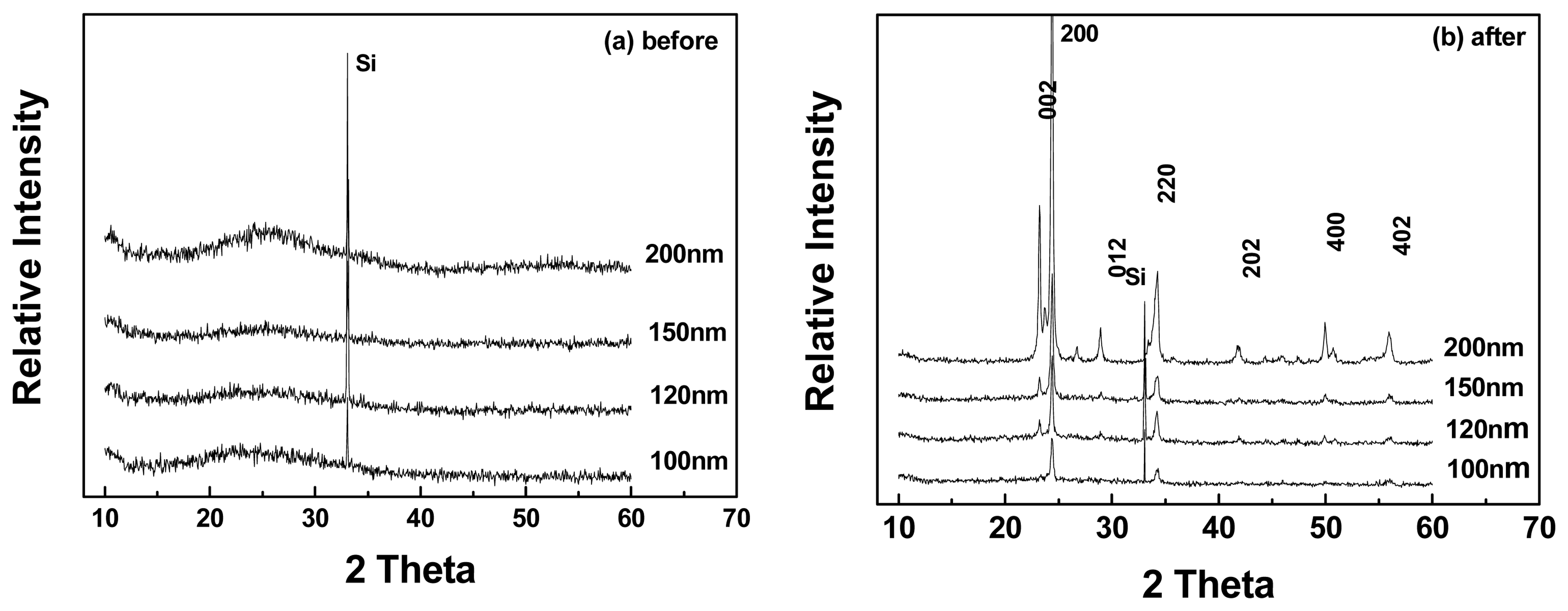
Fig. 2 (a) and (b) shows the X-ray diffraction pattern of various thickness deposited WO
3 thin films before and after heat treatment at 500°C for 30minuts in air. Regardless of thickness, the as-deposited WO
3 thin films were existed in an amorphous phase and no other peaks except a Si(100) peak at 33° (2θ) and a broad peak between 20-30° (2θ) were observed. After annealing, WO
3 phase was grown into polycrystalline with increasing intensity, indicating a major peak (200) and other minor peaks in various directions. The obtained XRD peaks were in accordance with JCPDS data card No.83-0951 of WO
3. Similar results of XRD were obtained when different mol% of NiO was deposited onto the WO
3 films. It was difficult to distinguish NiO-WO
3 thin film structure except the (002) peak tended stronger. The NiO phase was not detected by XRD since the amount of NiO is less and below the detection limit of the instrument.
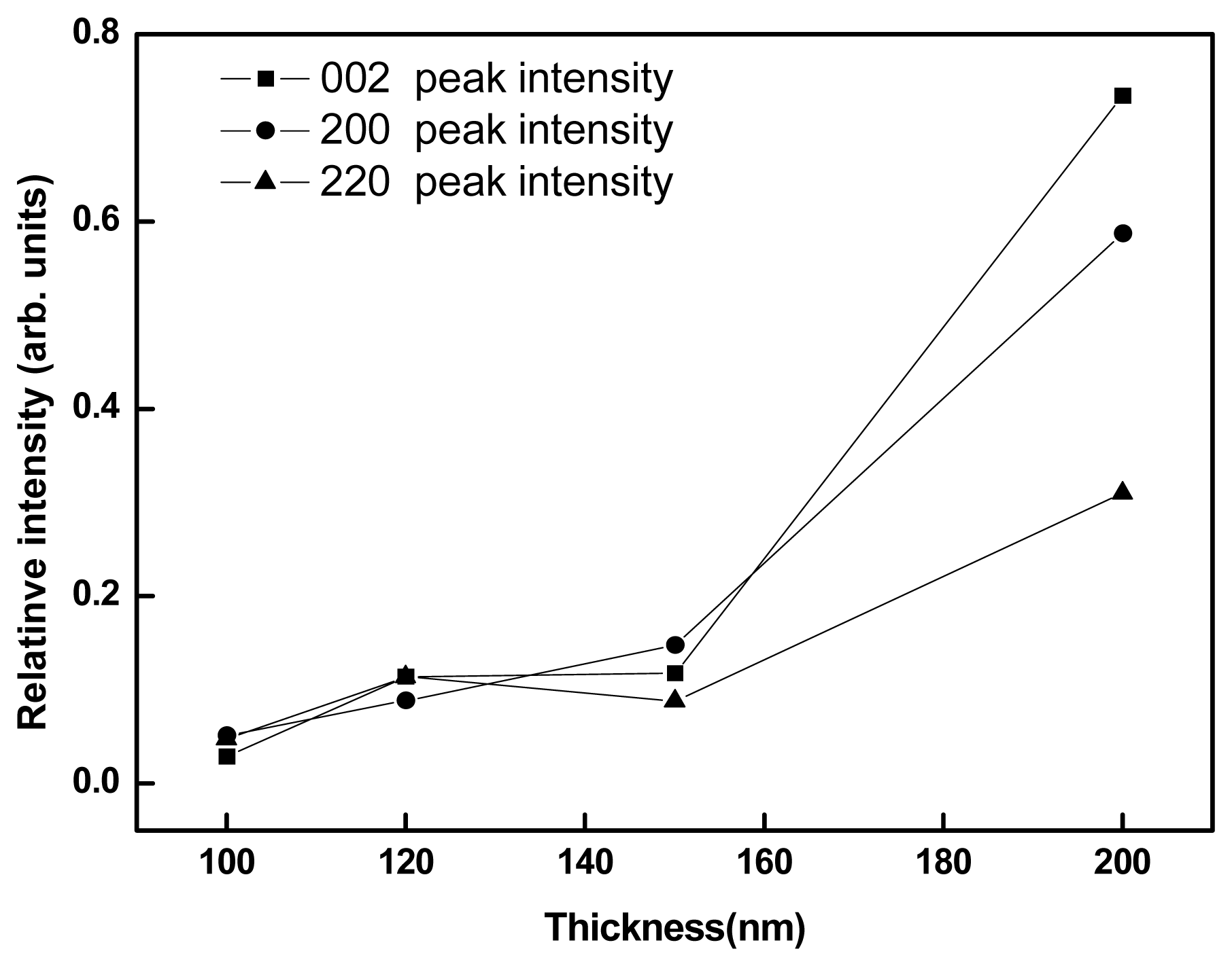
Fig. 3 shows the variation of XRD peak intensities as a function of thickness for pure WO
3 films after annealing. The major peak intensities were almost equal up to 150 nm WO
3 thickness, however, between 150-200 nm thickness the intensities of (220), (200) and (002) peaks were steeply increased. Similar effect was observed after NiO addition also.
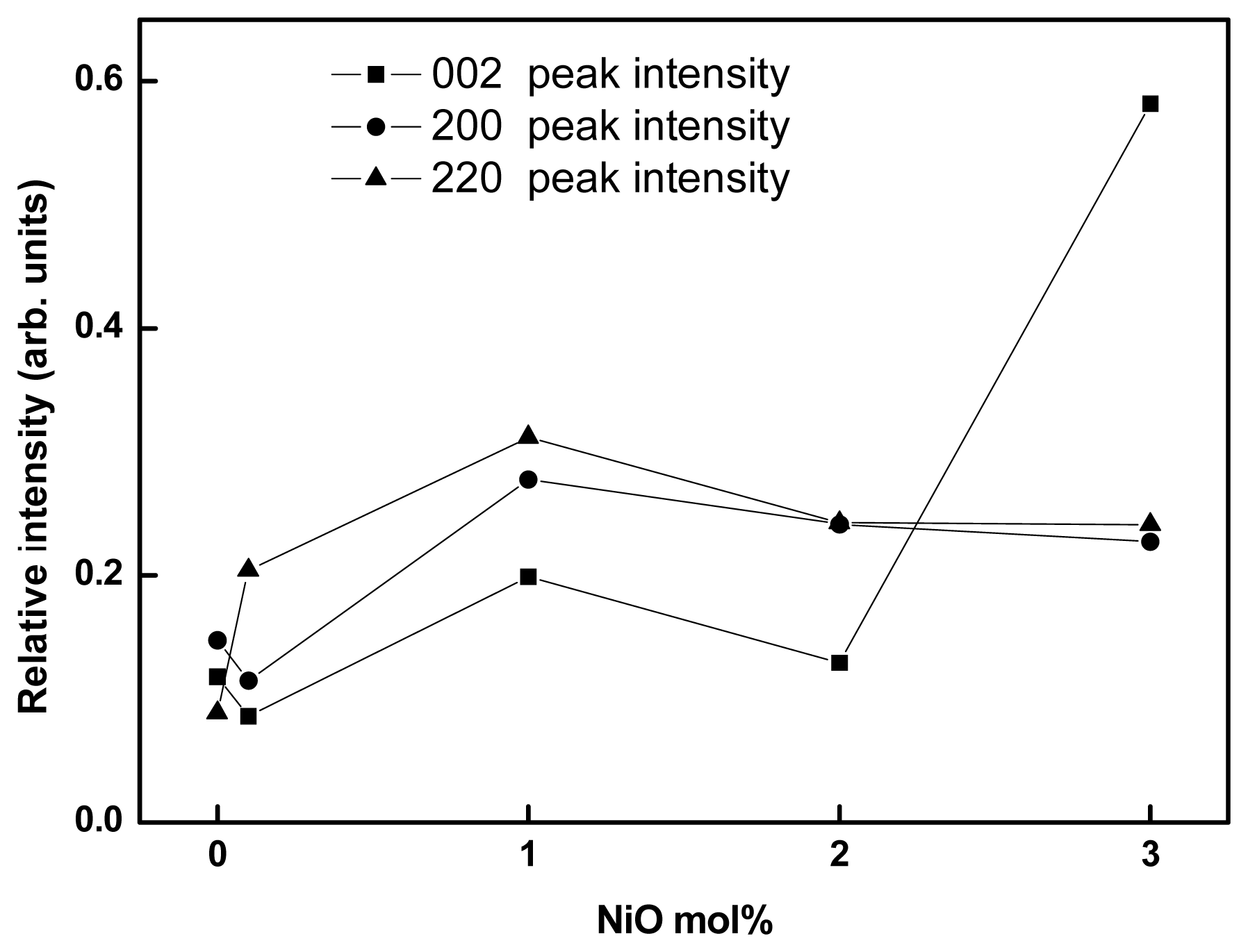
Fig. 4 shows the variation of peaks intensity as a function of NiO addition (mol%) on 150nm WO
3 film. Though there was no major change observed in peak intensities up to 2 mol% NiO addition, the intensity of (002) major peak was steeply increased with above 2 mol% of NiO addition, remaining the intensities of other peaks unchanged. The sudden increase in the peak intensity indicates a change in microstructure and film properties. The change in relative intensity was calculated as the ratio of the particular peak intensity to the sum of all intensities of the film according to
equation (1).
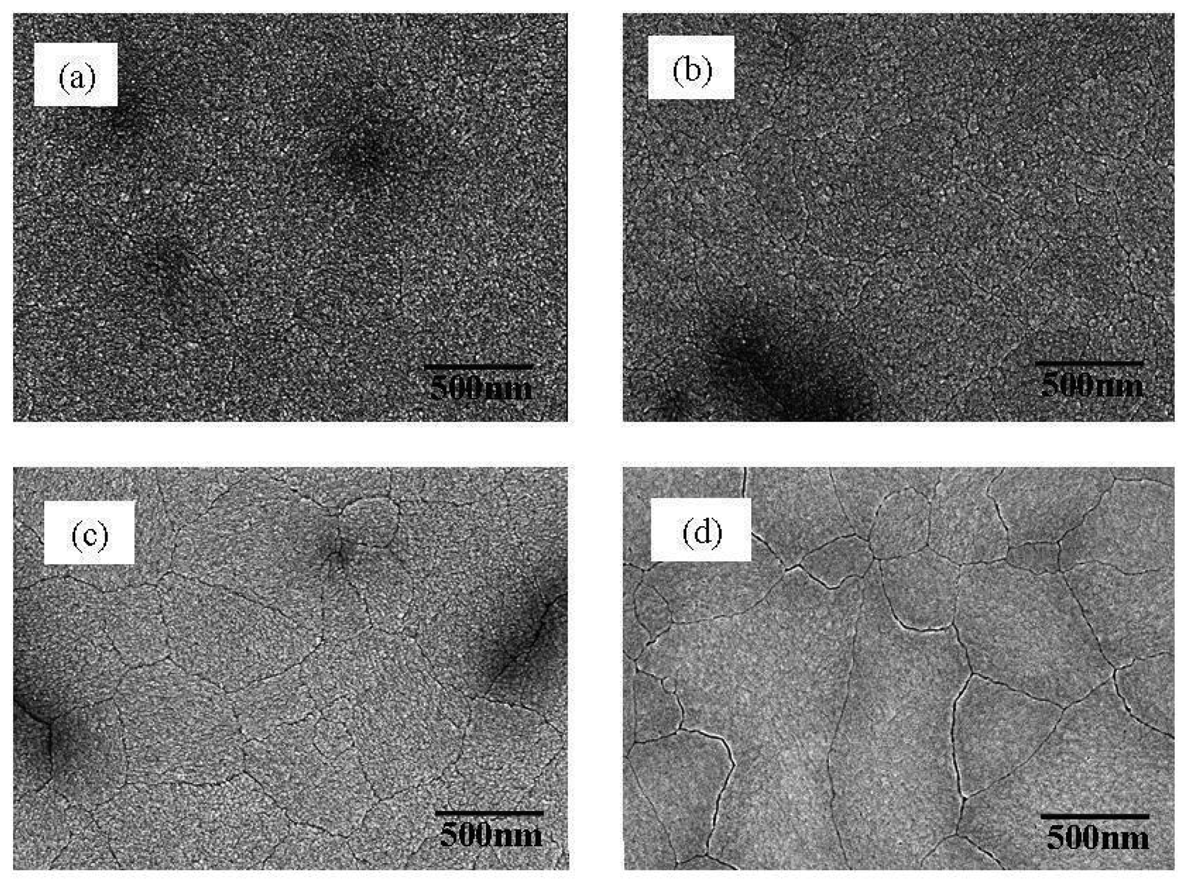
Fig. 5 shows the SEM micrographs of surface morphology and cross section of WO
3 thin films deposited for (a) 100 (b) 120 (c) 150 and (d) 200 nm thickness after annealing. The surface morphology is generally similar except with increased thickness. The average grain size of these films is about 0.5 μm. However, large polycrystalline grains were formed by the necking or merging of small grains during the annealing process. The cracks between the large grains could be formed as the small grains became closer and agglomerated at the annealing temperature, and got shrinkage while undergoing the cooling process. Large grains or crack gaps cause to decrease the surface area and connectivity of films and to deteriorate film properties of electronic materials. It can be observed that crack gaps were increased with increasing film thickness.
The grain growth was effectively inhibited by depositing NiO on WO
3 thin film surfaces.
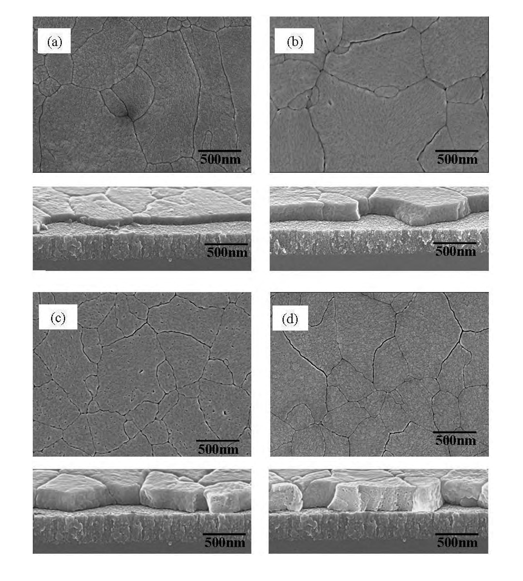
Fig. 6 (a-d) shows the surface morphology after a fixed amount of NiO (0.0009g, equivalent to 1.0, 0.75, 0.5 and 0.25 mol%) was deposited onto the respective films of 100, 120, 150 and 200nm (0.25, 0.5, 0.75, 1.0g weight) WO
3 films. NiO deposition was found to be inhibited the grain growth in only 100 and 120 nm films (
a, b), but not in 150 and 200nm WO
3 films (
c, d) as observed in the figure. Moreover, the crack gap was increased with WO
3 thickness above 120nm. It means that 1.0-0.75mol% NiO addition could effectively able to control the surface cracks of 100-120nm thickness WO
3 films, and below or above this critical range of NiO and WO
3 thickness, surface cracks were not inhibited as seen in
Figs. 6 (c) and (d). Thus, this is one limitation of inhibition of grain growth in NiO deposited WO
3 thin films.
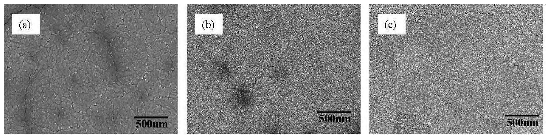
Similarly, by fixing WO
3 thickness, NiO content was varied. 1-3 mol% of NiO was deposited on 150nm WO
3 thin films and observed SEM surface morphologies as in
Fig. 7 (a-c). It is observed that 1-2 mol% NiO added films contain small and uniform grain size (
Fig. a, b) but 3 mol% NiO added surface (
Fig. c) depicts indistinct large grains. This is because, 1-2 mol% NiO is forming small island like structures penetrating the inter-granules of WO
3 and suppress the formation of large grains. But in case of 3mol%, NiO is becoming excess and forming like a thin continuous layer over WO
3 surface and could not penetrate into the inter-granules of WO
3.
It can be deduced from the above two results that, the grain growth was not inhibited in 150nm thickness WO
3 films if the content of NiO is less than 0.75 mol% and more than 2 mol% as seen in
Figs. 6 (c) and
Fig. 7 (c). It can only be controlled if the addition of NiO is between 1-2 mol% as shown in
Fig. 7(a) and (b). Hence, the inhibition is limited to a certain thickness of WO
3 (100-150 nm) and NiO content (0.75-2 mol%) of inclusion, and below or above this limitation the cracks could not be suppressed. This inference is in quite coincidence with the XRD peak intensity patterns observed in
Fig.3 and
Fig.4.
Further, the deposition sequence of NiO on WO3 is also having an effect on the surface properties as shown in
Fig. 8. The deposition of NiO beneath WO3 film (
Fig.8a) could not inhibit any grain growth. Whereas NiO deposition on both sides of the WO3 film (
Fig.8b) could control the cracks to some extent by forming island like structures on WO
3 surface as observed from the figure. Hence, it can be implied that an optimum NiO deposition above WO
3 film is only the most effective process to suppress the grain growth of WO
3 films.
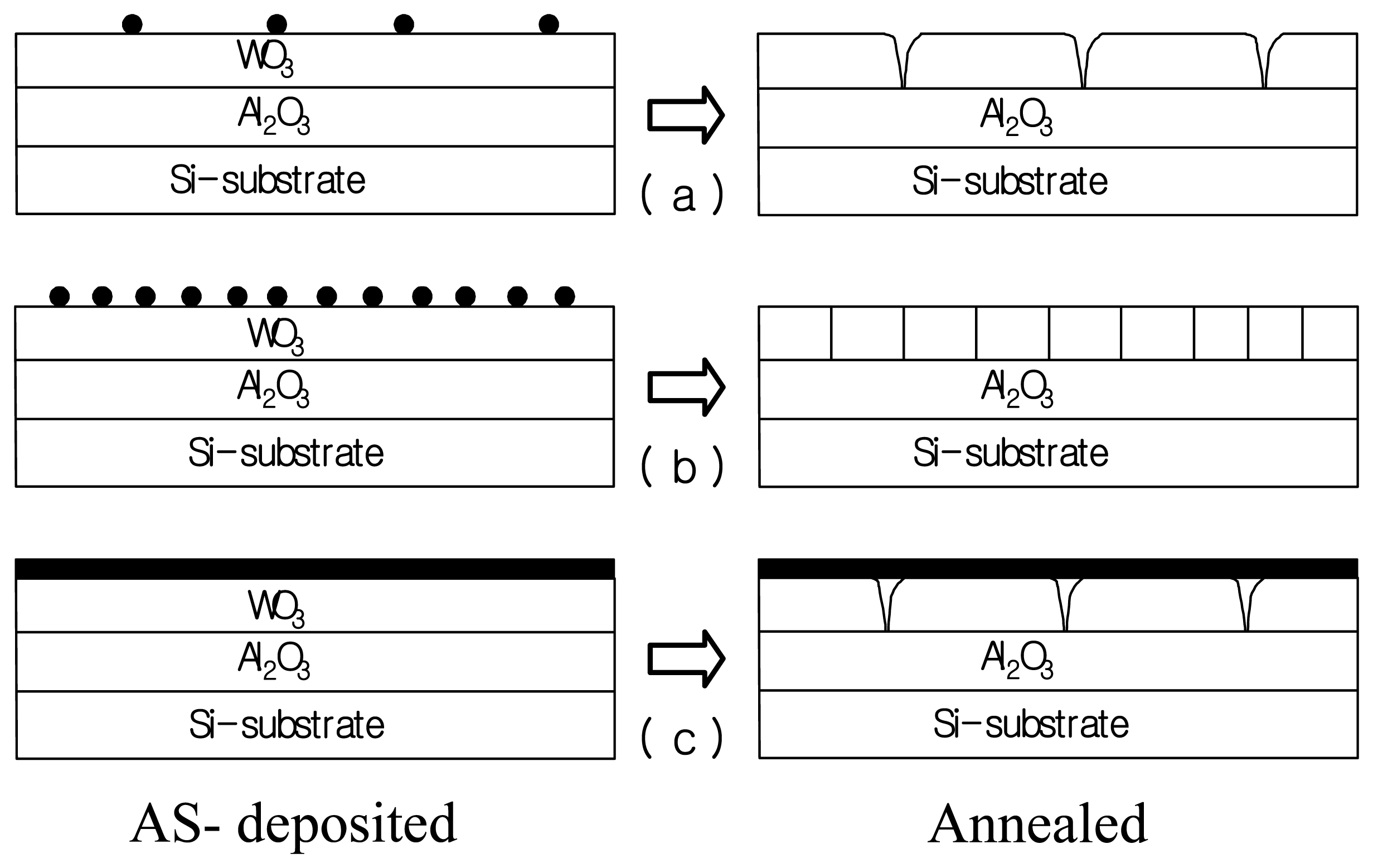
The mechanism involved in inhibition of grain growths by deposition of NiO on the WO
3 thin film surface is illustrated in
Fig. 9. During normal course of annealing large grains will be forming on WO
3 surface due to material diffusion and merging effects. However, less amount of NiO deposition can not control the grain growth as they are widely dispersed and insufficient on WO
3 surface (
Fig. a). Similarly, excess amount of NiO leads to the formation of a thin continuous layer over WO
3 surface leaving them uncontrolled underneath (
Fig. c). But an optimum amount of NiO in proportion to the WO
3 film thickness could only suppress the grain growth by interfering into the inter-granules with sufficient NiO-WO
3 correlation (
Fig. b).
WO
3 thin films were found to be one of the best candidates to detect NO
x gas. However, the sensitivity to NO
x gas was comparatively not so high.
Fig. 10 shows the change in resistances with time when 5 ppm NO
2 gas was passed onto the various surface of (a) pure WO
3 (150nm) (b) NiO(1mol%):WO
3 (150nm) (c) NiO(0.5mol%):WO
3(150nm) and (d) NiO(3mol%):WO
3(150nm) thin films. 150nm pure WO
3 thin film was able to detect a change of 40×10
6ohms in resistance at 250°C operating temperature. Whereas NiO(1mol%) deposited WO
3 thin film has shown a change more than that of one order of the pure WO
3 film at the same NO
2 concentration. This reflects the improvement in sensitivity of the 1 mol % NiO:WO
3 thin film as NO
2 sensor. On the other hand, the fast response and recovery characteristics of the sensor were also be observed from
Fig. 10 (b).
Similarly, the change of resistance of the NO
2 sensor when the NiO addition is less or more of the critical limit was depicted in
Fig. 10 (c) and (d). In both the cases the sensing property was much deteriorated due to the surface defects as compared to that of
Fig. 10 (b).
