Development of Gentle Slope Light Guide Structure in a 3.4 μm Pixel Pitch Global Shutter CMOS Image Sensor with Multiple Accumulation Shutter Technology †

 , ,
, ,
Abstract
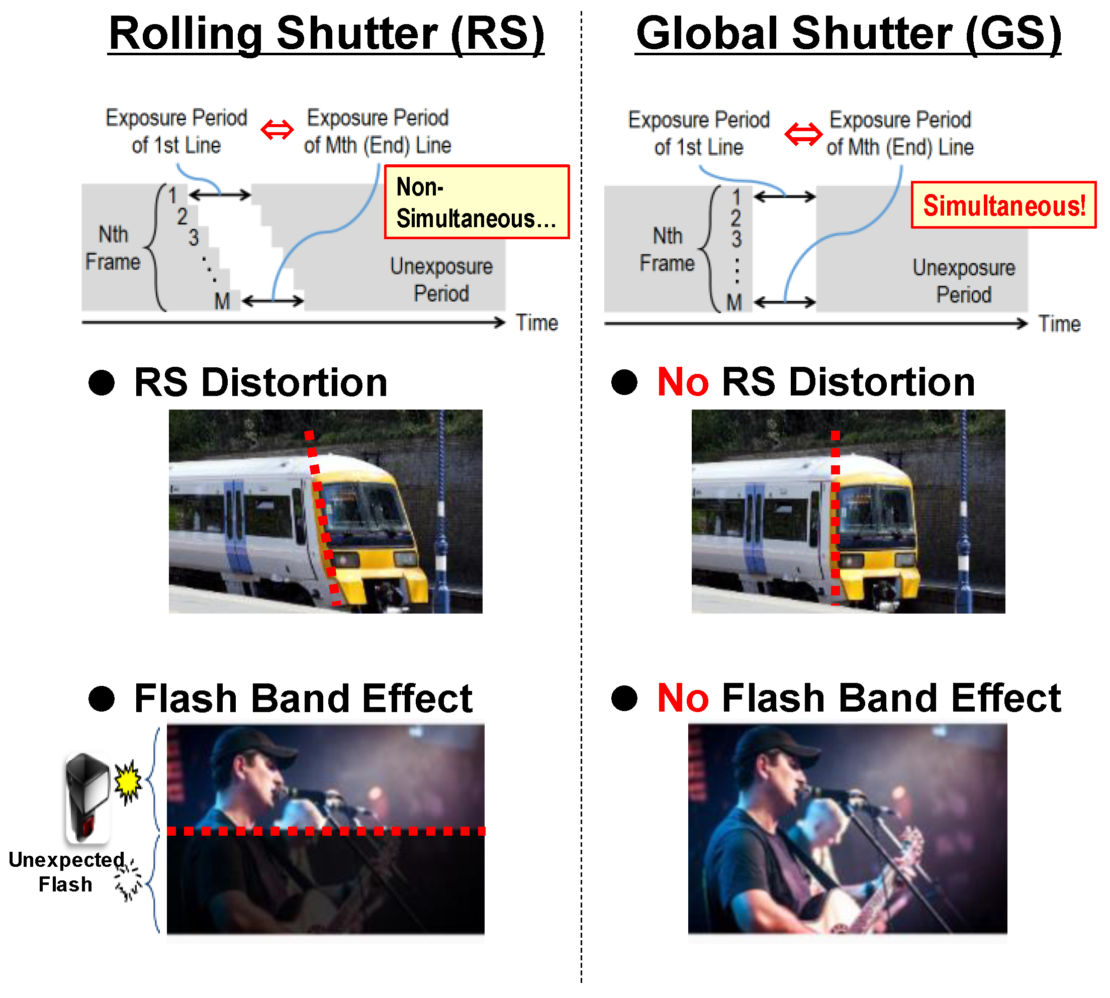
:1. Introduction
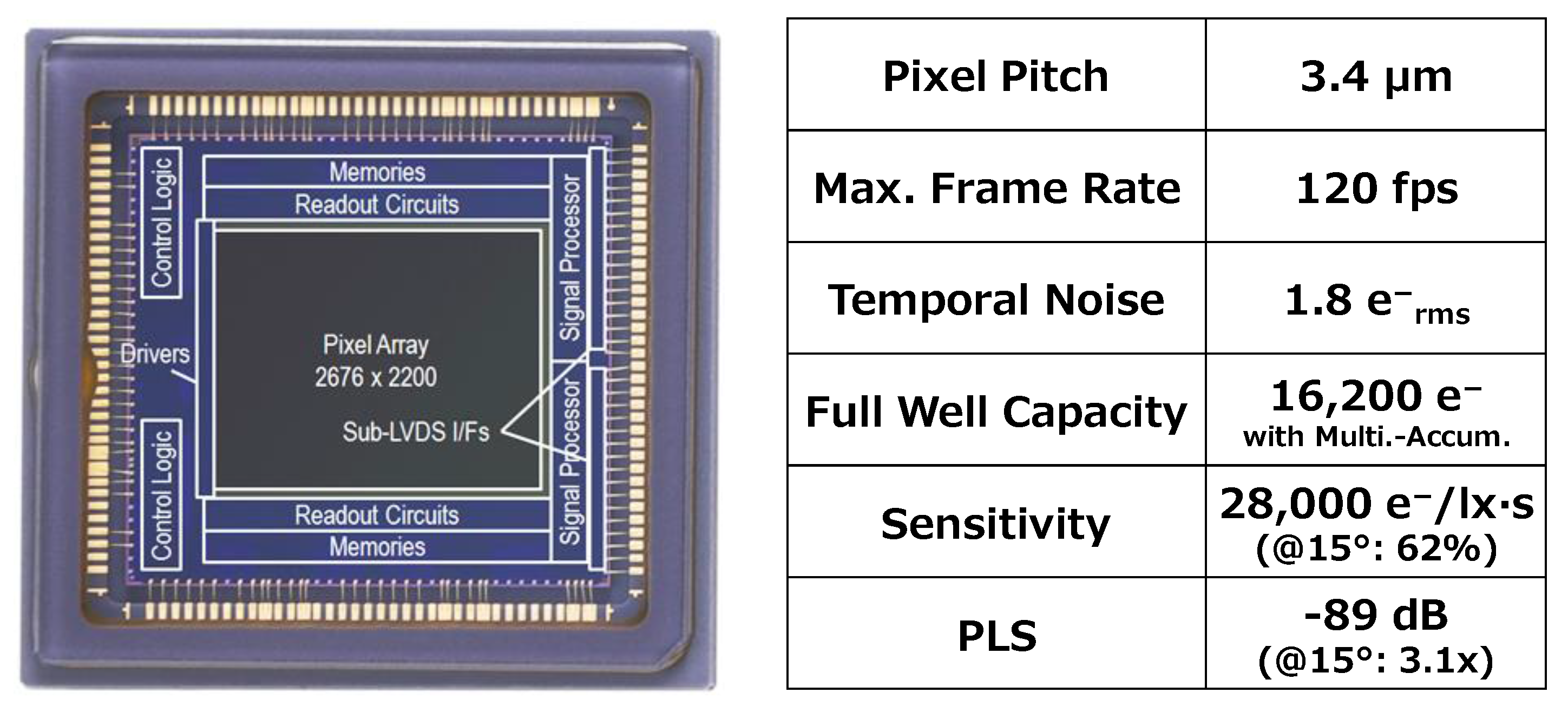
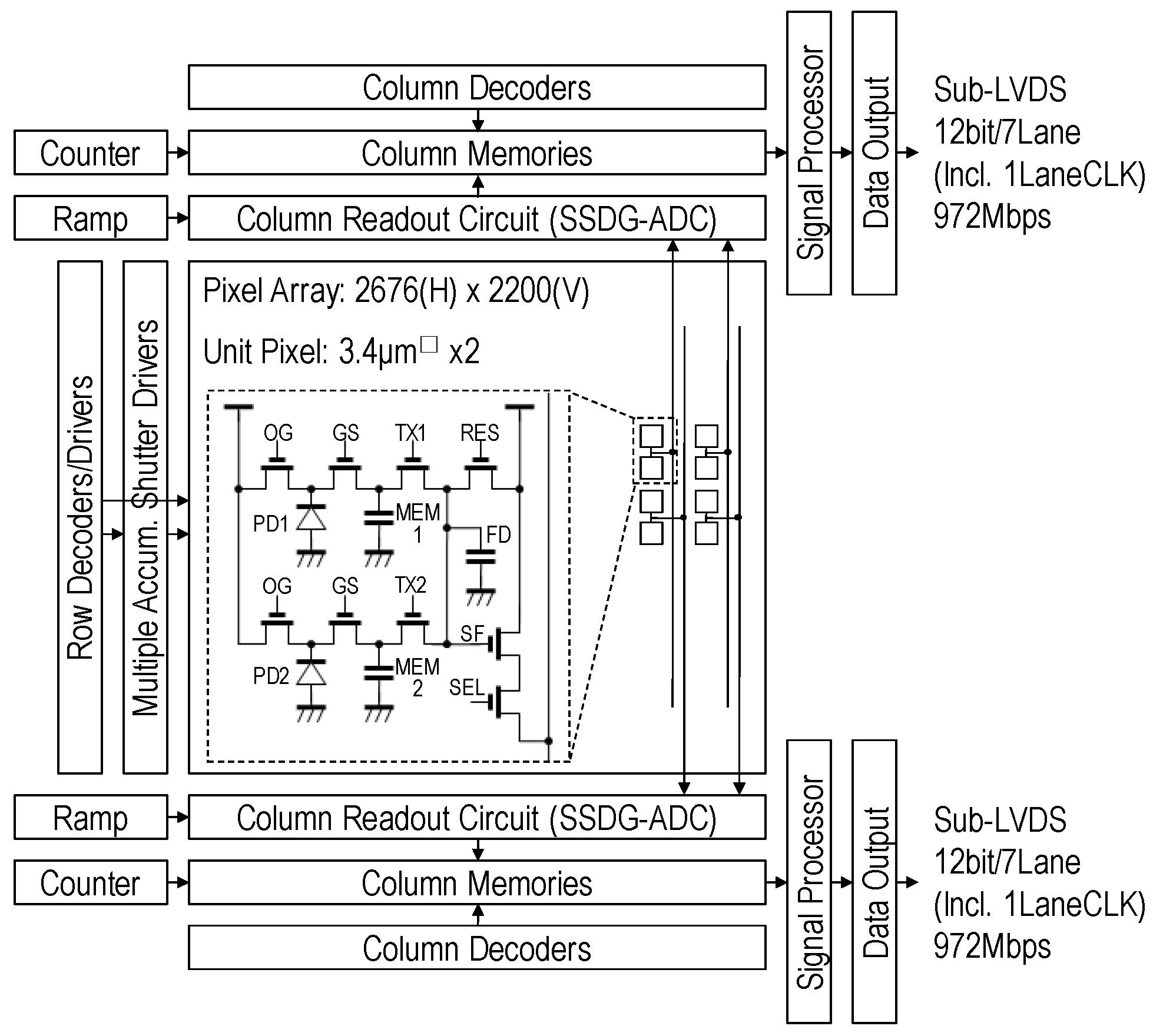
2. Sensor Architecture
3. Our Technology
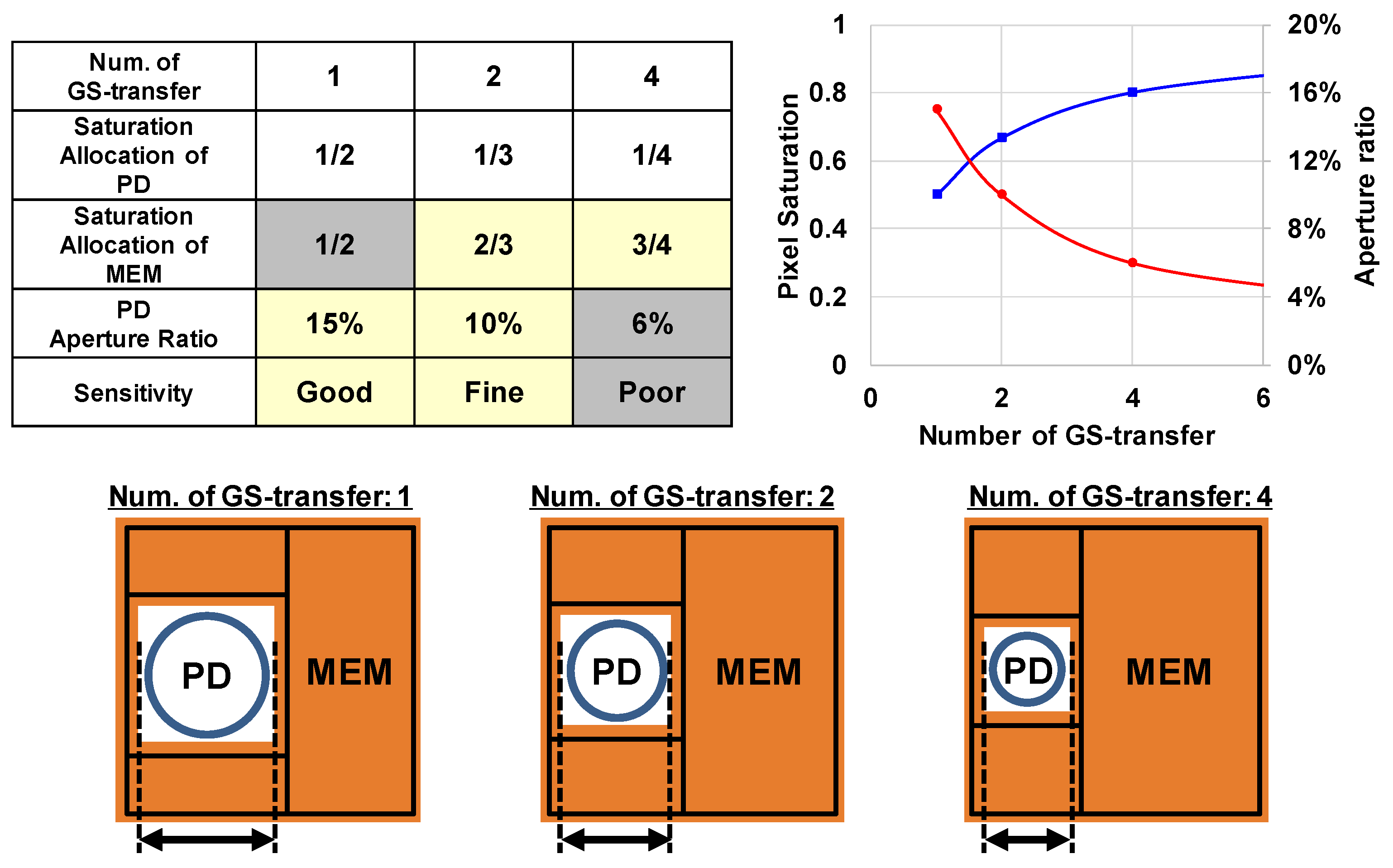
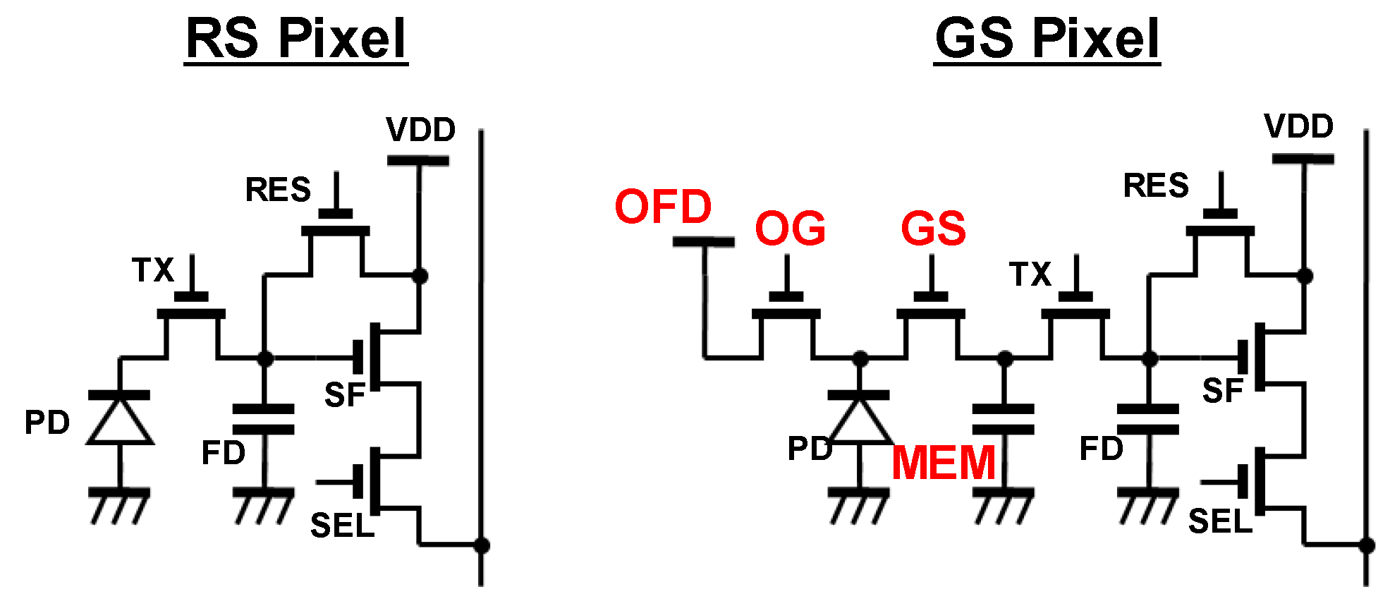
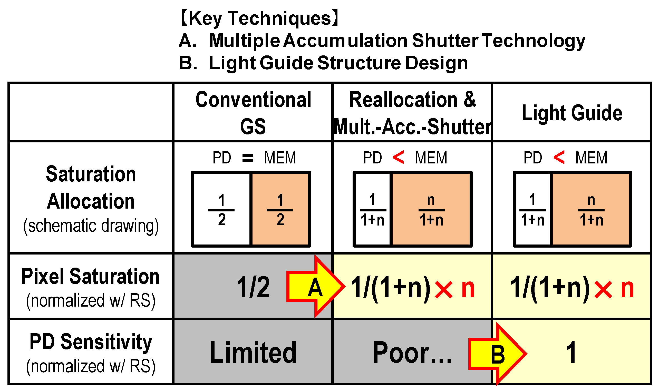
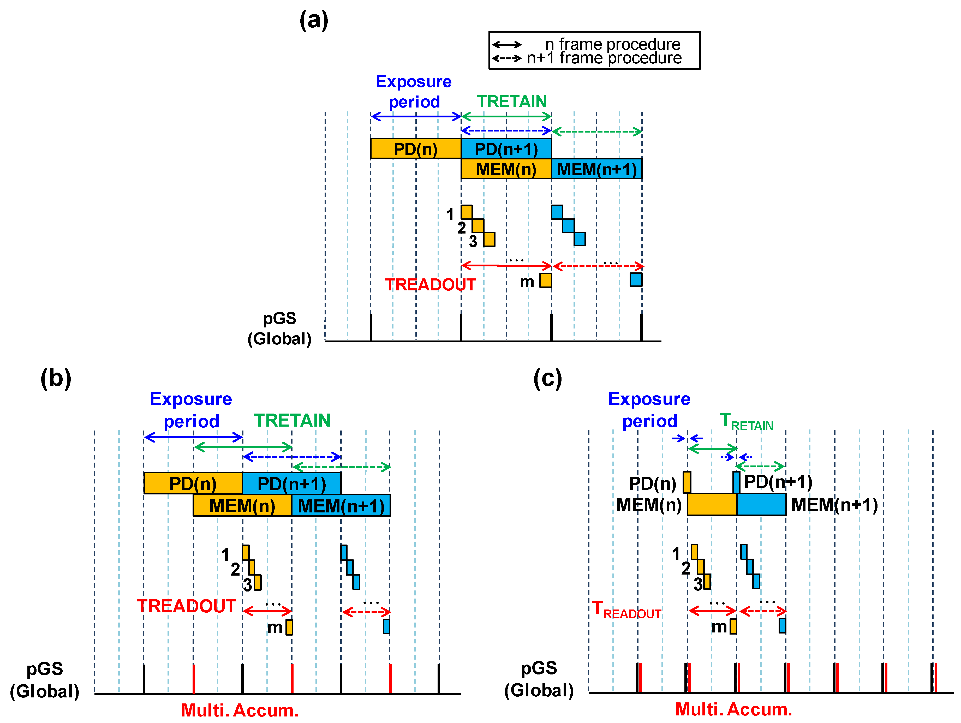
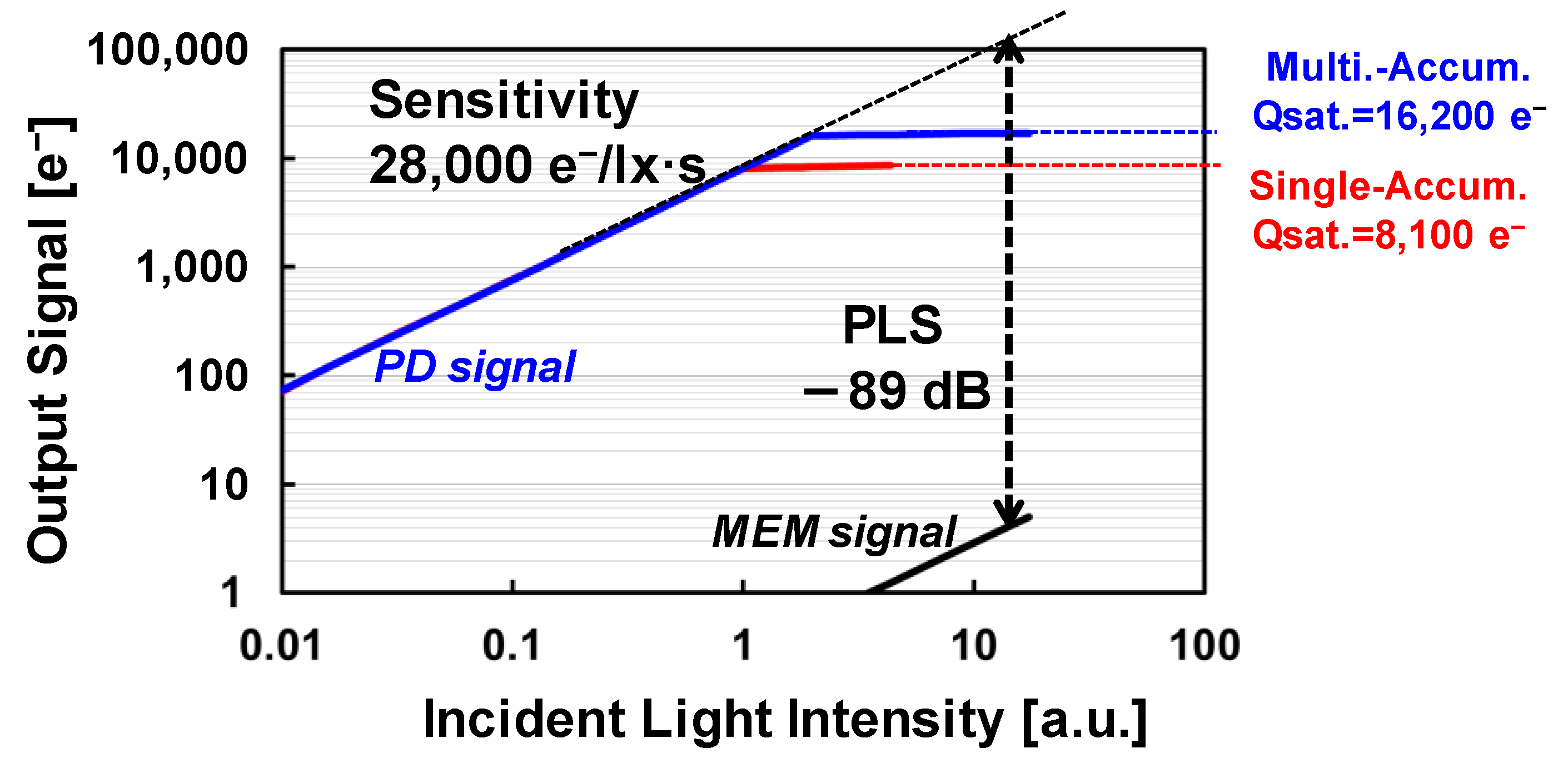
3.1. Multiple Accumulation Shutter Technology
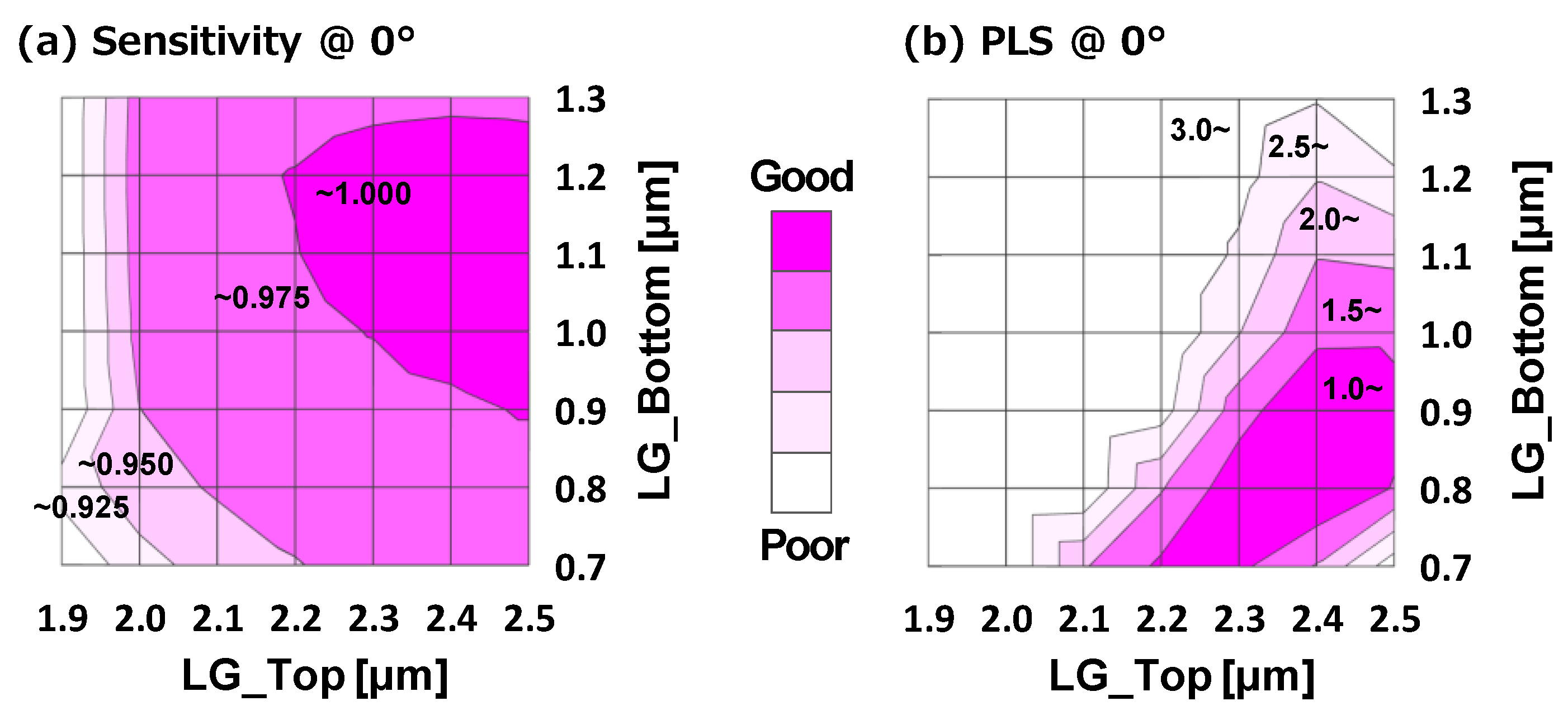
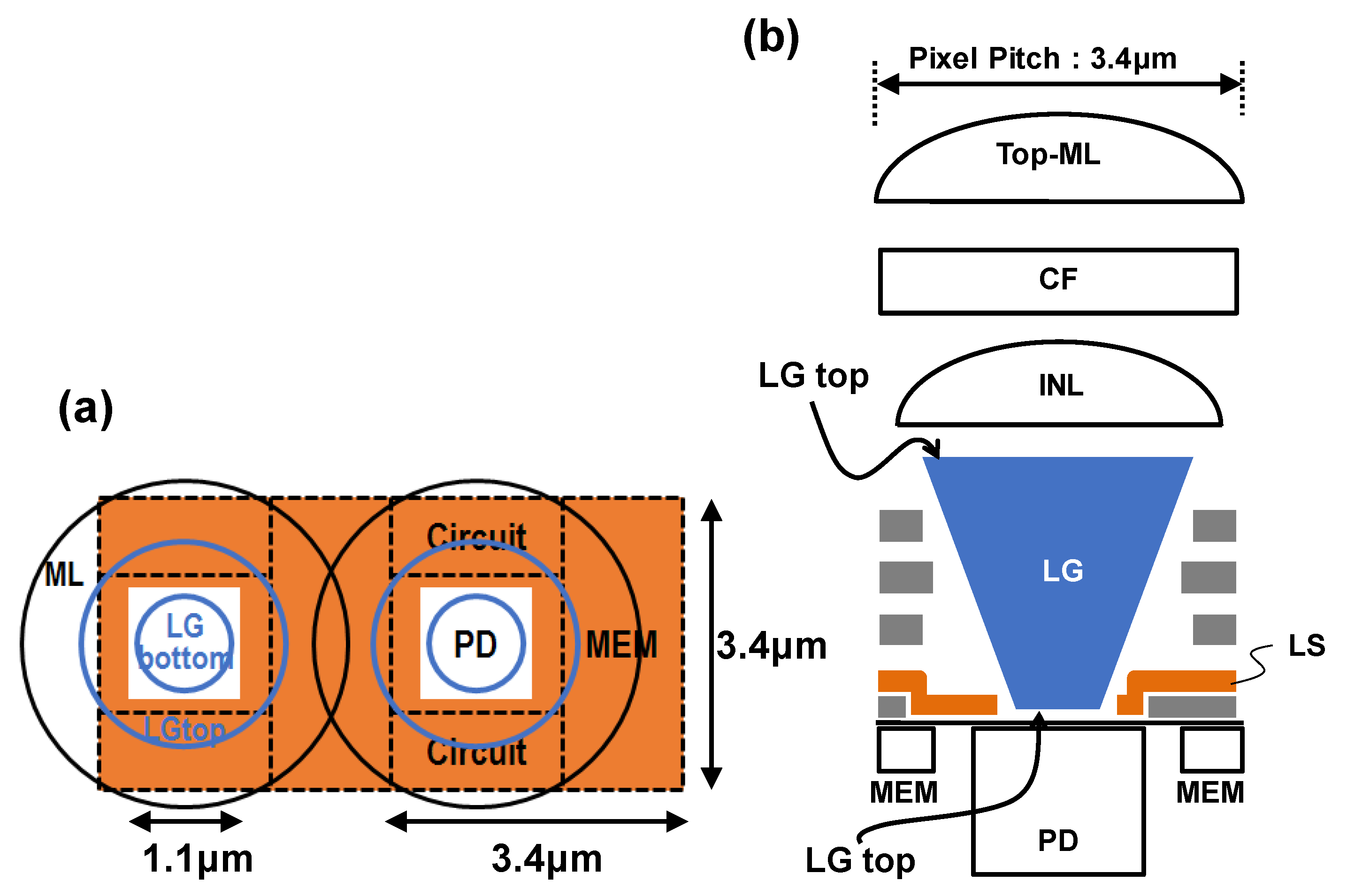
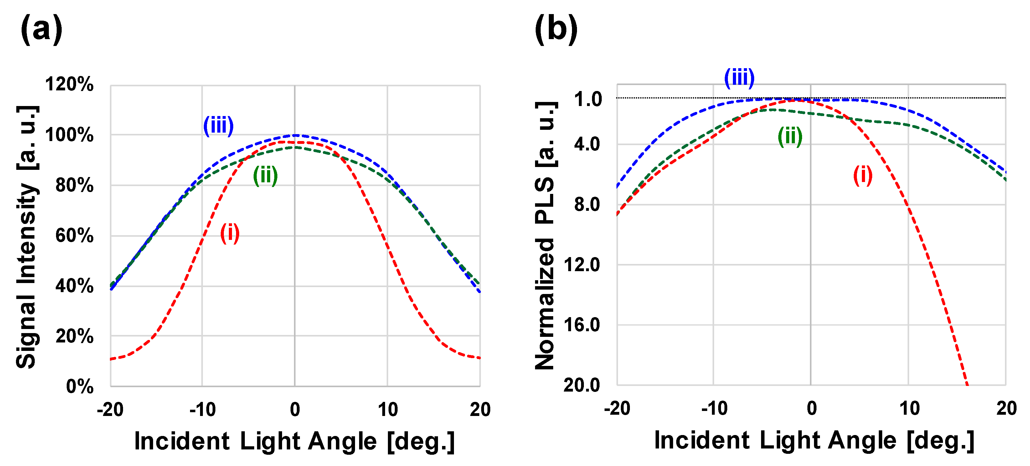
3.2. Light Guide Structure Design
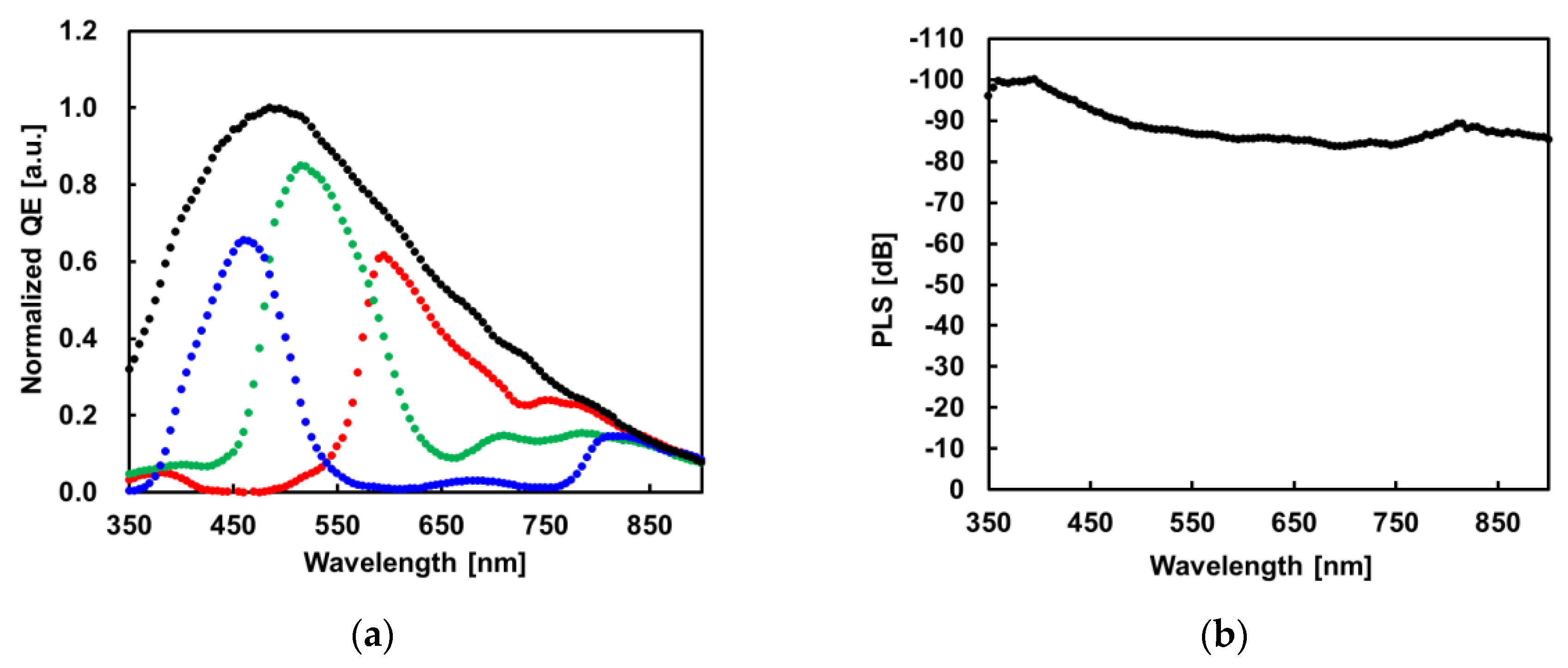
4. Experimental Results
5. Conclusions
Acknowledgments
Author Contributions
Conflicts of Interest
References
- Yasutomi, K.; Seo, M.W.; Kamoto, M.; Teranishi, N.; Kawahito, S. A 0.61 E-Noise Global Shutter CMOS Image Sensor with Two-Stage Charge Transfer Pixels. In Proceedings of the 2017 Symposium on VLSI Circuits, Kyoto, Japan, 5–8 June 2017. [Google Scholar] [CrossRef]
- Sakano, Y.; Sakai, S.; Tashiro, Y.; Kato, Y.; Akiyama, K.; Honda, K.; Sato, M.; Sakakibara, M.; Taura, T.; Azami, K.; et al. 224-ke Saturation Signal Global Shutter CMOS Image Sensor with In-Pixel Pinned Storage and Lateral Overflow Integration Capacitor. In Proceedings of the 2017 Symposium on VLSI Circuits, Kyoto, Japan, 5–8 June 2017. [Google Scholar] [CrossRef]
- Velichko, S.; Agranov, G.; Hynecek, J.; Johnson, S.; Komori, H.; Bai, J.; Karasev, I.; Mauritzson, R.; Yi, X.; Lenchenkov, V.; et al. Low Noise High Efficiency 3.75 μm and 2.8 μm Global Shutter CMOS Pixel Arrays. In Proceedings of the 2013 International Image Sensor Workshop (IISW), Sandy, UT, USA, 12–16 June 2013. [Google Scholar]
- Yokoyama, T.; Suzuki, M.; Nishi1, Y.; Mizuno, I.; Lahav, A. Design of Double micro lens structure for 2.8 µm Global Shutter Pixel. In Proceedings of the 2017 International Image Sensor Workshop (IISW), Hiroshima, Japan, 30 May–2 June 2017; pp. 398–401. [Google Scholar]
- Kawabata, K.; Kobayashi, M.; Onuki, Y.; Sekine, H.; Tsuboi, T.; Matsuno, Y.; Takahashi, H.; Inoue, S.; Ichikawa, T. A 1.8e− Temporal Noise Over 90 dB Dynamic Range 4k2k Super 35 mm format Seamless Global Shutter CMOS Image Sensor with Multiple Accumulation Shutter Technology. In Proceedings of the IEEE International Electron Devices Meeting (IEDM), San Francisco, CA, USA, 3–7 December 2016; pp. 216–218. [Google Scholar]
- Kobayashi, M.; Onuki, Y.; Kawabata, K.; Sekine, H.; Tsuboi, T.; Matsuno, Y.; Takahashi, H.; Koizumi, T.; Sakurai, K.; Yuzurihara, H.; et al. A 1.8erms− Temporal Noise Over 110dB Dynamic Range 3.4μm Pixel Pitch Global Shutter CMOS Image Sensor with Dual-Gain Amplifiers SS-ADC and Multiple Accumulation Shutter. In Proceedings of the IEEE International Solid-State Circuits Conference (ISSCC), San Francisco, CA, USA, 5–9 February 2017; pp. 74–75. [Google Scholar]
- Sekine, H.; Kobayashi, M.; Onuki, Y.; Kawabata, K.; Tsuboi, T.; Matsuno, Y.; Takahashi, H.; Inoue, S.; Ichikawa, T. A High Optical Performance 3.4 μm Pixel Pitch Global Shutter CMOS Image Sensor with Light Guide Structure. In Proceedings of the 2017 International Image Sensor Workshop (IISW), Hiroshima, Japan, 30 May–2 June 2017; pp. 394–397. [Google Scholar]
- Totsuka, H.; Tsuboi, T.; Muto, T.; Yoshida, D.; Matsuno, Y.; Ohmura, M.; Takahashi, H.; Sakurai, K.; Ichikawa, T.; Yuzurihara, H.; et al. An APS-H size 250 Mpixel CMOS Image Sensor using Column Single Slope ADCs with Dual Gain Amplifiers. In Proceedings of the IEEE International Solid-State Circuits Conference (ISSCC), San Francisco, CA, USA, 31 January–4 February 2016; pp. 116–117. [Google Scholar]
- Oike, Y.; Akiyama, K.; Hung, L.D.; Niitsuma, W.; Kato, A.; Sato, M.; Kato, Y.; Nakamura, W.; Shiroshita, H.; Sakano, Y.; et al. An 8.3 M-pixel 480 fps Global-Shutter CMOS Image Sensor with Gain-Adaptive Column ADCs and 2-on-1 Stacked Device Structure. In Proceedings of the IEEE Symposium on VLSI Circuits (VLSI-Circuits), Honolulu, HI, USA, 15–17 June 2016; pp. 222–223. [Google Scholar]
- Centen, P.; Lehr, S.; Roth, S.; Rotte, J.; Heizmann, F.; Momin, A.; Dohmen, R.; Schaaf, K.; Damstra, J.; Ree, R.; et al. A 4e-noise 2/3-inch Global Shutter 1920x1080P120 CMOS-Imager. In Proceedings of the 2013 International Image Sensor Workshop (IISW), Sandy, UT, USA, 12–16 June 2013. [Google Scholar]


| (i) Non-LG | (ii) Steep LG | (iii) Gentle LG | ||
|---|---|---|---|---|
| Top diameter | - | 2.0 | 2.4 | |
| Bottom diameter | - | 0.8 | 0.8 | |
| Taper | - | Steep | Gentle | |
| Signal Intensity | @ 0° | 98% | 97% | 100% |
| @ 15° | 21% | 62% | 62% | |
| Normalized PLS | @ 0° | 1.2× | 2.7× | 1.0× |
| @ 15° | 16.7× | 4.0× | 3.1× | |
| Unit | This work | [5] IEDM 2016 | [9] VLSI 2016 | [10] IISW 2013 | |||
|---|---|---|---|---|---|---|---|
| Shutter Function | - | GS | GS | GS | GS | ||
| Pixel Pitch | μm | 3.4 | 6.4 | 5.86 | 5.0 | ||
| Number of Effective Pixels | - | 2592 × 2054 | 4046 × 2496 | 3840 × 2164 | 1920 × 1080 | ||
| Maximum Frame Rate | fps | 120 | 30 | 60 | 90 | 480 | 240 |
| Full Well Capacity | e− | 1620 | 70,000 | 38,000 | 19,000 | 30,450 | 15,000 |
| e−/µm2 | 1380 | 1700 | 930 | 460 | 890 | 600 | |
| Sensitivity | e−/lx·s | 28,000 | 80,000 | 17,500 | 54,250 | ||
| e−/lx·s/um2 | 2420 | 1950 | 510 | 2170 | |||
| Temporal Noise | e−rms | 1.8 | 1.8 | 4.6 | 4.0 | ||
| Dynamic Range | dB | 79.0 | 92.0 | 86.0 | 80.0 | 76.3 | 71.5 |
| Parasitic Light Sensitivity | dB | −89 | −78 | −100 | −70 | ||
| Power Consumption | W | 0.45 | 1.5 | 5.23 | 1.1 | ||
| Figure of Merit 1 | e−·nJ | 1.27 | 8.91 | 4.46 | 2.23 | 6.04 | 8.84 |
| Figure of Merit 2 | e−·nJ | 0.14 | 0.23 | 0.21 | 0.21 | 0.92 | 2.36 |
© 2017 by the authors. Licensee MDPI, Basel, Switzerland. This article is an open access article distributed under the terms and conditions of the Creative Commons Attribution (CC BY) license (http://creativecommons.org/licenses/by/4.0/).
Share and Cite
Sekine, H.; Kobayashi, M.; Onuki, Y.; Kawabata, K.; Tsuboi, T.; Matsuno, Y.; Takahashi, H.; Inoue, S.; Ichikawa, T. Development of Gentle Slope Light Guide Structure in a 3.4 μm Pixel Pitch Global Shutter CMOS Image Sensor with Multiple Accumulation Shutter Technology. Sensors 2017, 17, 2860. https://doi.org/10.3390/s17122860
Sekine H, Kobayashi M, Onuki Y, Kawabata K, Tsuboi T, Matsuno Y, Takahashi H, Inoue S, Ichikawa T. Development of Gentle Slope Light Guide Structure in a 3.4 μm Pixel Pitch Global Shutter CMOS Image Sensor with Multiple Accumulation Shutter Technology. Sensors. 2017; 17(12):2860. https://doi.org/10.3390/s17122860
Chicago/Turabian StyleSekine, Hiroshi, Masahiro Kobayashi, Yusuke Onuki, Kazunari Kawabata, Toshiki Tsuboi, Yasushi Matsuno, Hidekazu Takahashi, Shunsuke Inoue, and Takeshi Ichikawa. 2017. "Development of Gentle Slope Light Guide Structure in a 3.4 μm Pixel Pitch Global Shutter CMOS Image Sensor with Multiple Accumulation Shutter Technology" Sensors 17, no. 12: 2860. https://doi.org/10.3390/s17122860