
A Flexible Arrayed Eddy Current Sensor for Inspection of Hollow Axle Inner Surfaces

Abstract
:1. Introduction
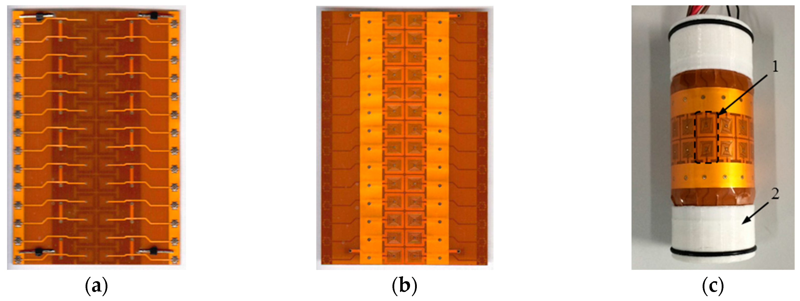
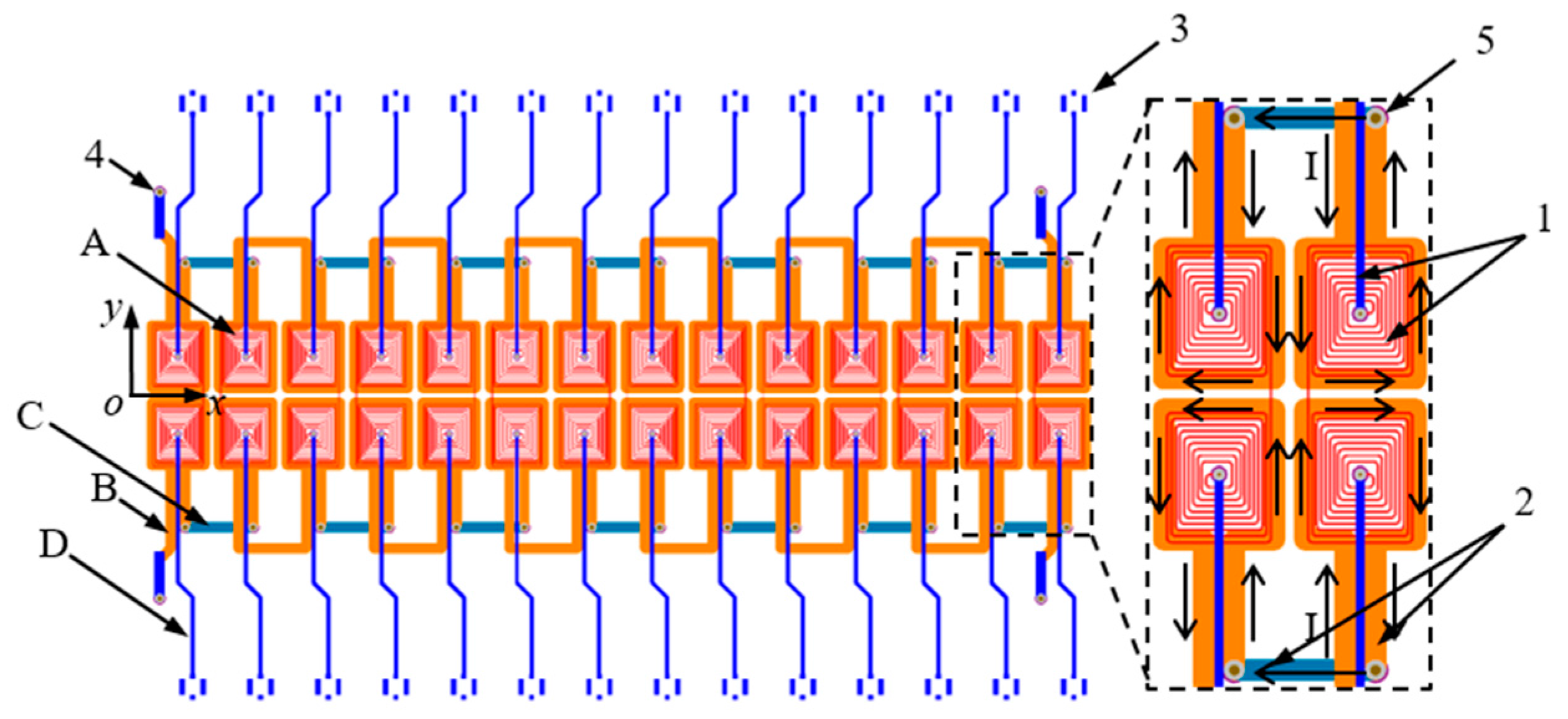
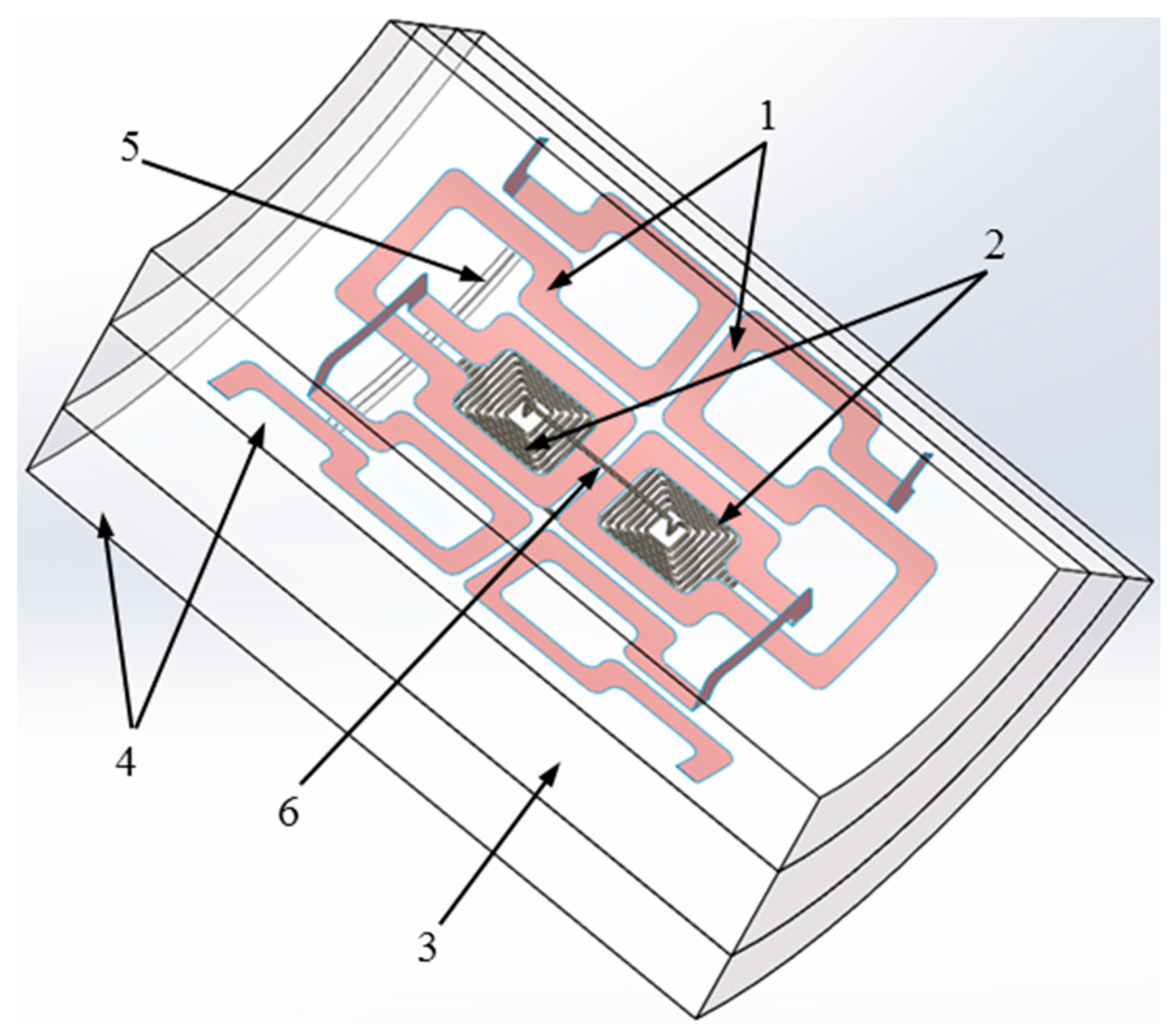
2. Sensor Design
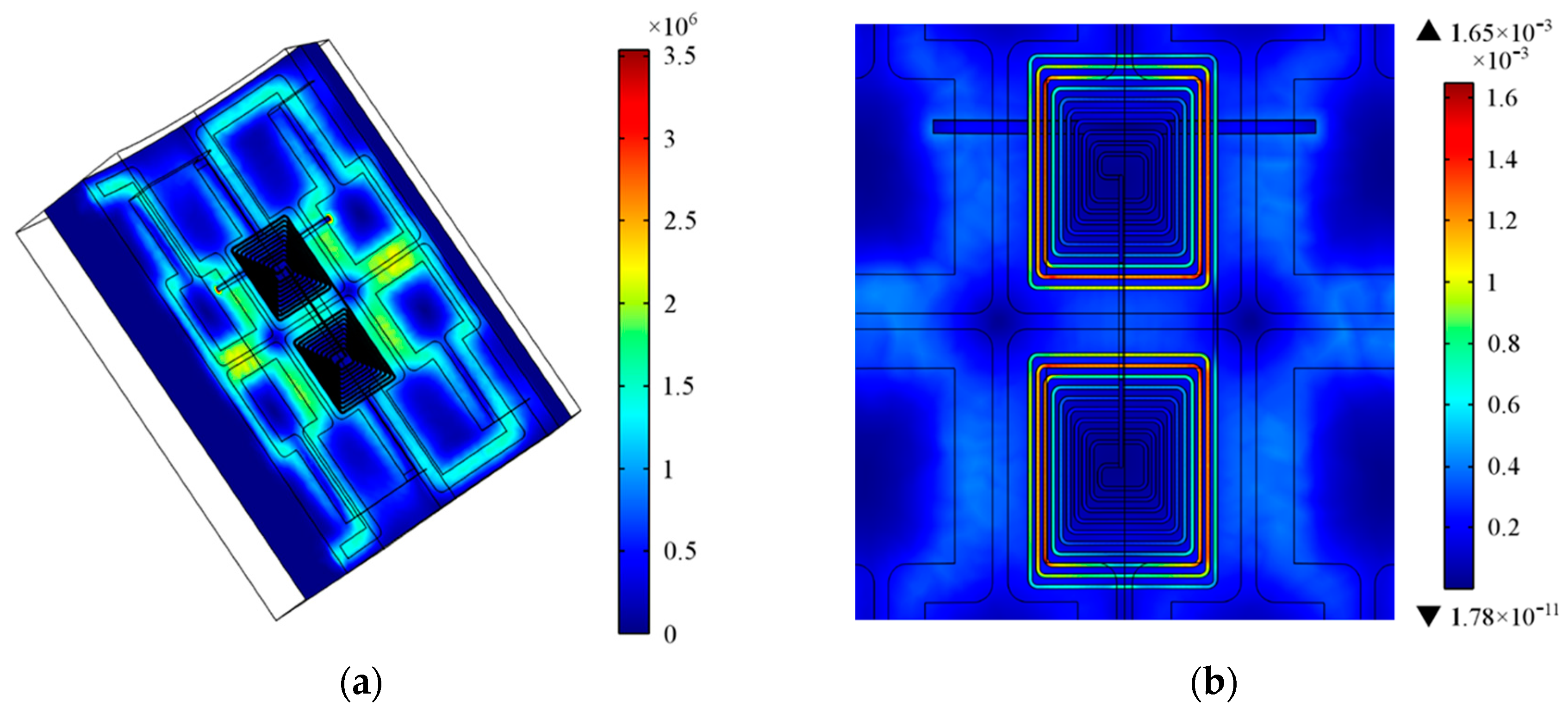
3. Finite Element Modeling
4. Experimental Validation
4.1. Experimental Set-up
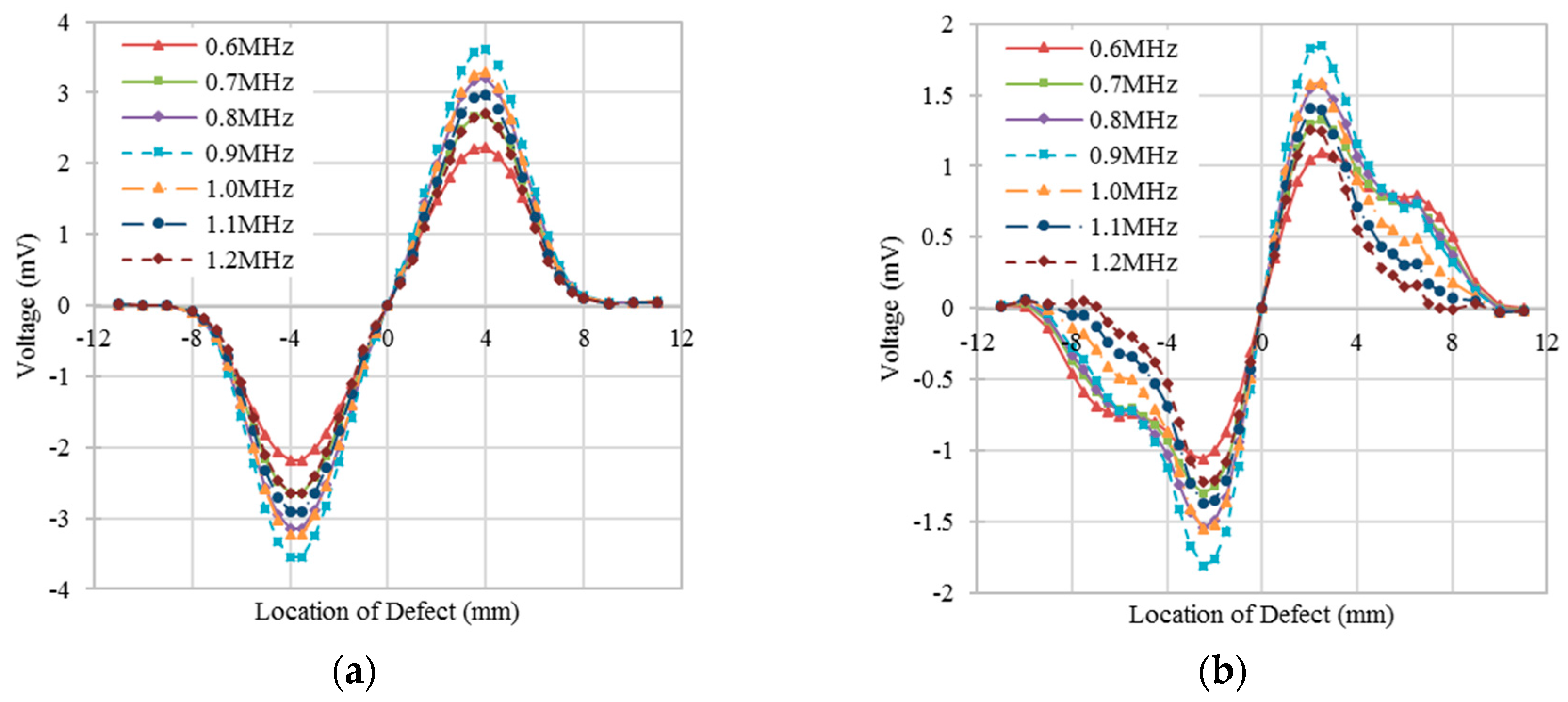
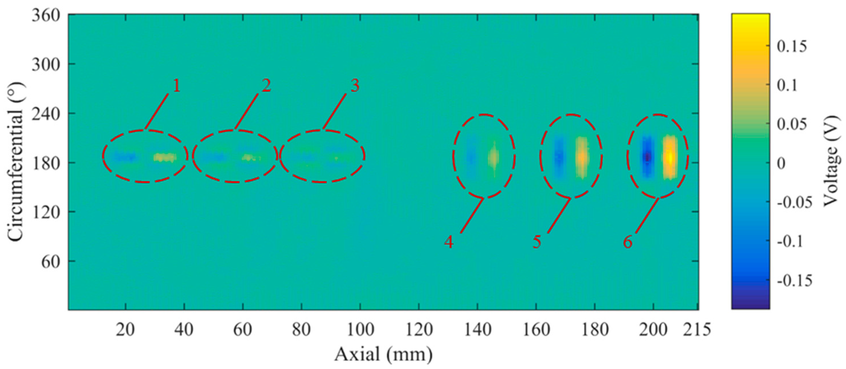
4.2. Experimental Results
5. Conclusions
Author Contributions
Conflicts of Interest
References
- Marty, P.N.; Engl, G.; Krafft, S.; Spinelli, J.M. Latest development in the UT inspection of train wheels and axles. In Proceedings of the 18th World Conference on Nondestructive Testing, Durban, South Africa, 16–20 April 2012.
- Carboni, M.; Cantini, S. Advanced ultrasonic “Probability of Detection” curves for designing in-service inspection intervals. Int. J. Fatigue 2016, 86, 77–87. [Google Scholar] [CrossRef]
- Rudlin, J.; Raude, A.; Völz, U.; Conte, A.L. New methods of rail axle inspection and assessment. In Proceedings of the 18th World Conference on Nondestructive Testing, Durban, South Africa, 16–20 April 2012.
- Kappes, W.; Hentschel, D.; Oelschlägel, T. Potential improvements of the presently applied in-service inspection of wheelset axles. Int. J. Fatigue 2016, 86, 64–76. [Google Scholar] [CrossRef]
- Li, F.; Sun, X.; Qiu, J.; Zhou, L.; Li, H.; Meng, G. Guided wave propagation in high-speed train axle and damage detection based on wave mode conversion. Struct. Control. Health Monit. 2015, 22, 1133–1147. [Google Scholar] [CrossRef]
- Ziaja, A.; Cheng, L.; Radecki, R.; Packo, P.; Staszewski, W. Cylindrical guided wave approach for damage detection in hollow train axles. In Proceedings of the 10th International Workshop on Structural Health Monitoring, Palo Alto, CA, USA, 1–3 September 2015; pp. 2054–2061.
- Lin, J.; Lin, F.; Lin, C.; Zhang, K.; Yu, X. Hollow shaft array electromagnetic testing system based on integrated nondestructive testing techniques. In Electromagnetic Nondestructive Evaluation (XVIII); IOS Press: Washington, DC, USA, 2015; Volume 40, pp. 296–302. [Google Scholar]
- Cavuto, A.; Martarelli, M.; Pandarese, G.; Revel, G.M.; Tomasini, E.P. Experimental investigation by laser ultrasonics for high speed train axle diagnostics. Ultrasonics 2015, 55, 48–57. [Google Scholar] [CrossRef] [PubMed]
- Chady, T.; Psuj, G.; Kowalczyk, J.; Spychalski, I. Electromagnetic system for nondestructive evaluation of train hollow axles. In Proceedings of the 2013 Far East Forum on Nondestructive Evaluation/Testing: New Technology & Application, Szczecin, Poland, 17–20 June 2013.
- Bureau, J.; Ward, R.C.; Jenstead, W. Advances in eddy current array sensor technology. In Proceedings of the 18th World Conference on Nondestructive Testing, Shanghai, China, 25–28 October 2008.
- Lepage, B. Development of a flexible cross-wound eddy current array probe. Int. J. Appl. Electromagn. Mech. 2014, 45, 633–638. [Google Scholar]
- Marchand, B.; Decitre, J.M.; Sergeeva-Chollet, N.; Skarlatos, A. Development of flexible array eddy current probes for complex geometries and inspection of magnetic parts using magnetic sensors. In Proceedings of the Conference on Review of Progress in Quantitative Nondestructive Evaluation, Denver, CO, USA, 15–20 July 2012.
- Crouch, A.; Goyen, T.; Porter, P. New method uses conformable array to map external pipeline corrosion. Oil Gas. J. 2004, 102, 55–59. [Google Scholar]
- Sheiretov, Y.; Evans, L.; Schlicker, D.; Zilberstein, V.; Goldfine, N.; Sikorski, R. TBC characterization using magnetic and electric field sensors. In Proceedings of the ASME Turbo Expo 2007: Power for Land, Sea, and Air, Montreal, QC, Canada, 14–17 May 2007; pp. 97–103.
- Endo, H.; Nishimizu, A.; Tooma, M.; Ouchi, H.; Yoshida, I.; Nonaka, Y.; Otani, K. Signal evaluation system of flexible array ECT probes for inspecting complexly shaped surfaces. In Proceedings of the Conference on Review of Progress in Quantitative Nondestructive Evaluation, San Diego, CA, USA, 18–23 July 2010.
- Xie, R.; Chen, D.; Pan, M.; Tian, W.; Wu, X.; Zhou, W.; Tang, Y. Fatigue crack length sizing using a novel flexible eddy current sensor array. Sensors 2015, 15, 32138–32151. [Google Scholar] [CrossRef] [PubMed]
- García-Martín, J.; Gómez-Gil, J.; Vázquez-Sánchez, E. Non-destructive techniques based on eddy current testing. Sensors 2011, 11, 2525–2565. [Google Scholar] [CrossRef] [PubMed]


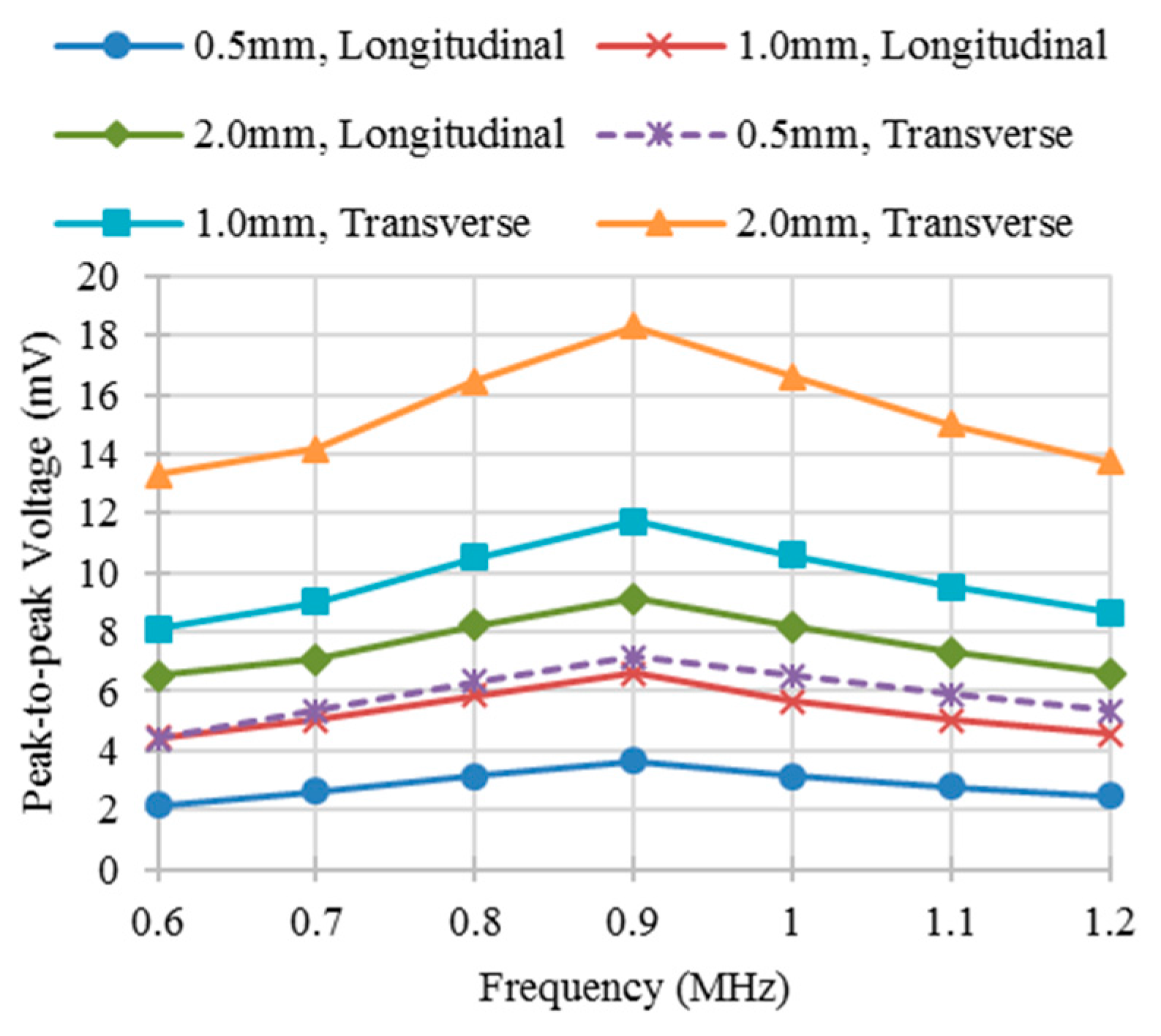
| Frequency (MHz) | 0.6 | 0.7 | 0.8 | 0.9 | 1.0 | 1.1 | 1.2 | |
|---|---|---|---|---|---|---|---|---|
| Defect Type | ||||||||
| 2.0 mm, longitudinal | 1.79 1 | 0.95 | 1.58 | 3.79 | 2.06 | 1.35 | 2.64 | |
| 1.0 mm, longitudinal | 2.14 | 2.23 | 0.75 | 2.20 | 2.17 | 2.23 | 2.71 | |
| 0.5 mm, longitudinal | 2.72 | 0.76 | 0.53 | 2.59 | 0.07 | 2.84 | 1.05 | |
| 2.0 mm, transverse | 1.28 | 1.54 | 1.43 | 3.14 | 1.35 | 2.38 | 0.76 | |
| 1.0 mm, transverse | 0.23 | 0.11 | 3.84 | 3.95 | 2.15 | 0.23 | 2.56 | |
| 0.5 mm, transverse | 1.59 | 2.29 | 0.31 | 3.44 | 2.83 | 2.84 | 2.06 | |
© 2016 by the authors; licensee MDPI, Basel, Switzerland. This article is an open access article distributed under the terms and conditions of the Creative Commons Attribution (CC-BY) license (http://creativecommons.org/licenses/by/4.0/).
Share and Cite
Sun, Z.; Cai, D.; Zou, C.; Zhang, W.; Chen, Q. A Flexible Arrayed Eddy Current Sensor for Inspection of Hollow Axle Inner Surfaces. Sensors 2016, 16, 952. https://doi.org/10.3390/s16070952
Sun Z, Cai D, Zou C, Zhang W, Chen Q. A Flexible Arrayed Eddy Current Sensor for Inspection of Hollow Axle Inner Surfaces. Sensors. 2016; 16(7):952. https://doi.org/10.3390/s16070952
Chicago/Turabian StyleSun, Zhenguo, Dong Cai, Cheng Zou, Wenzeng Zhang, and Qiang Chen. 2016. "A Flexible Arrayed Eddy Current Sensor for Inspection of Hollow Axle Inner Surfaces" Sensors 16, no. 7: 952. https://doi.org/10.3390/s16070952