
Active C4 Electrodes for Local Field Potential Recording Applications


Abstract
:
1. Introduction
2. Chip Design
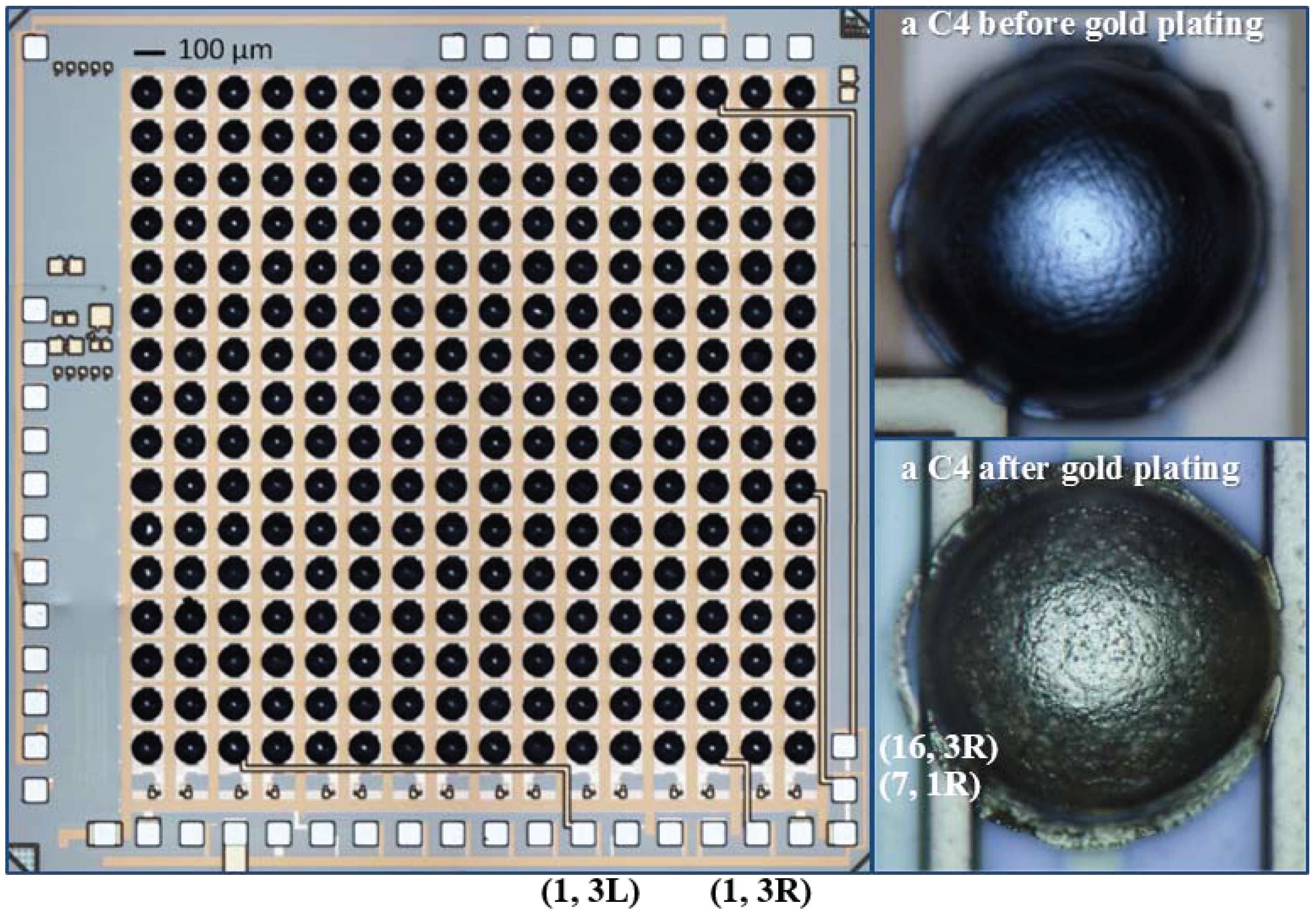
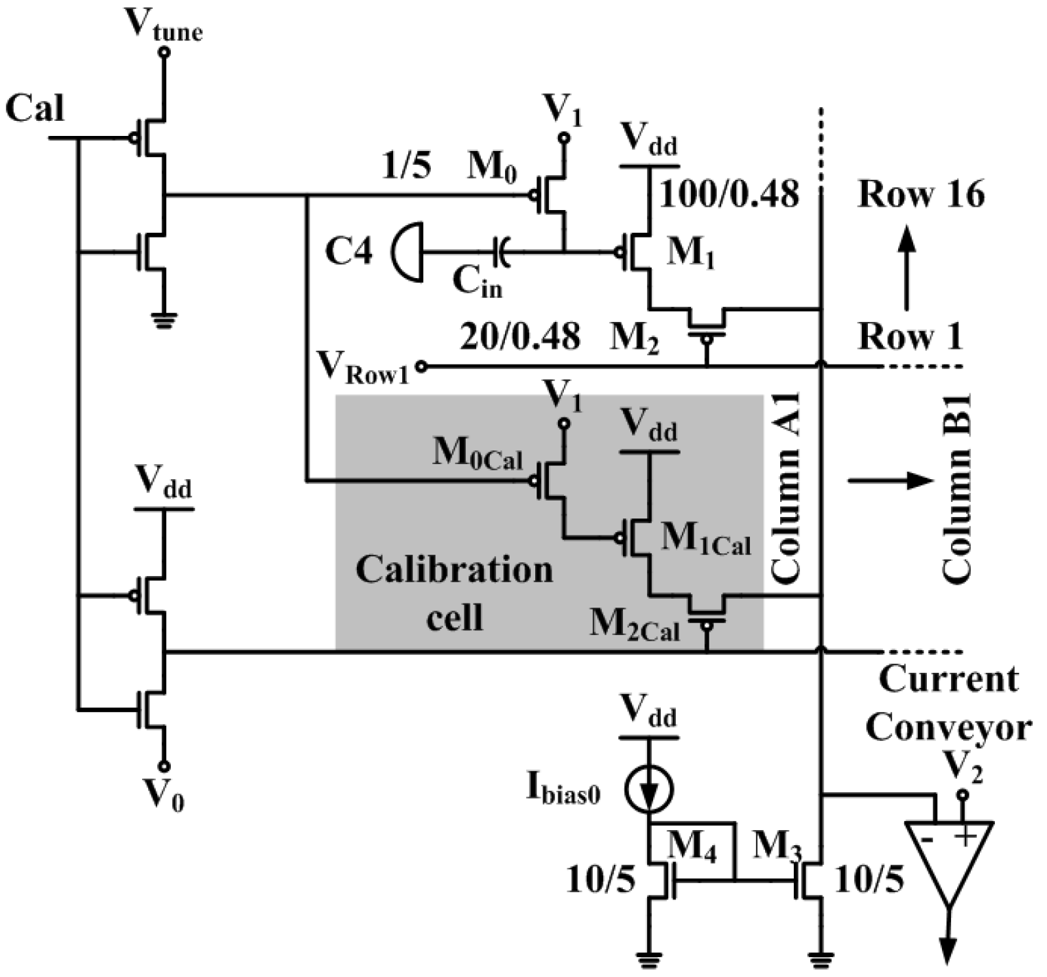
2.1. C4 Electrodes
2.2. Low-Noise Preamplifier
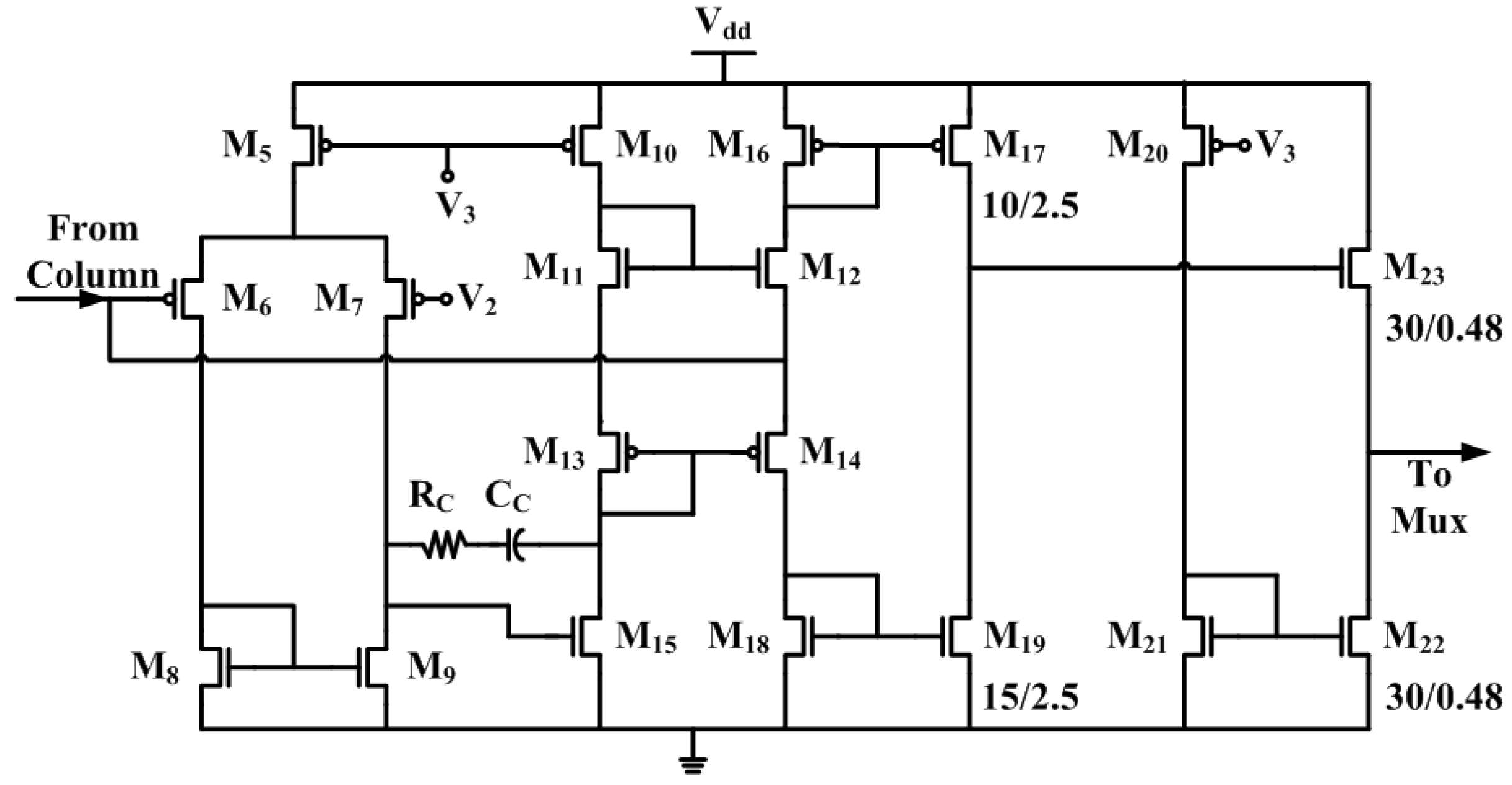
2.3. Current Conveyor
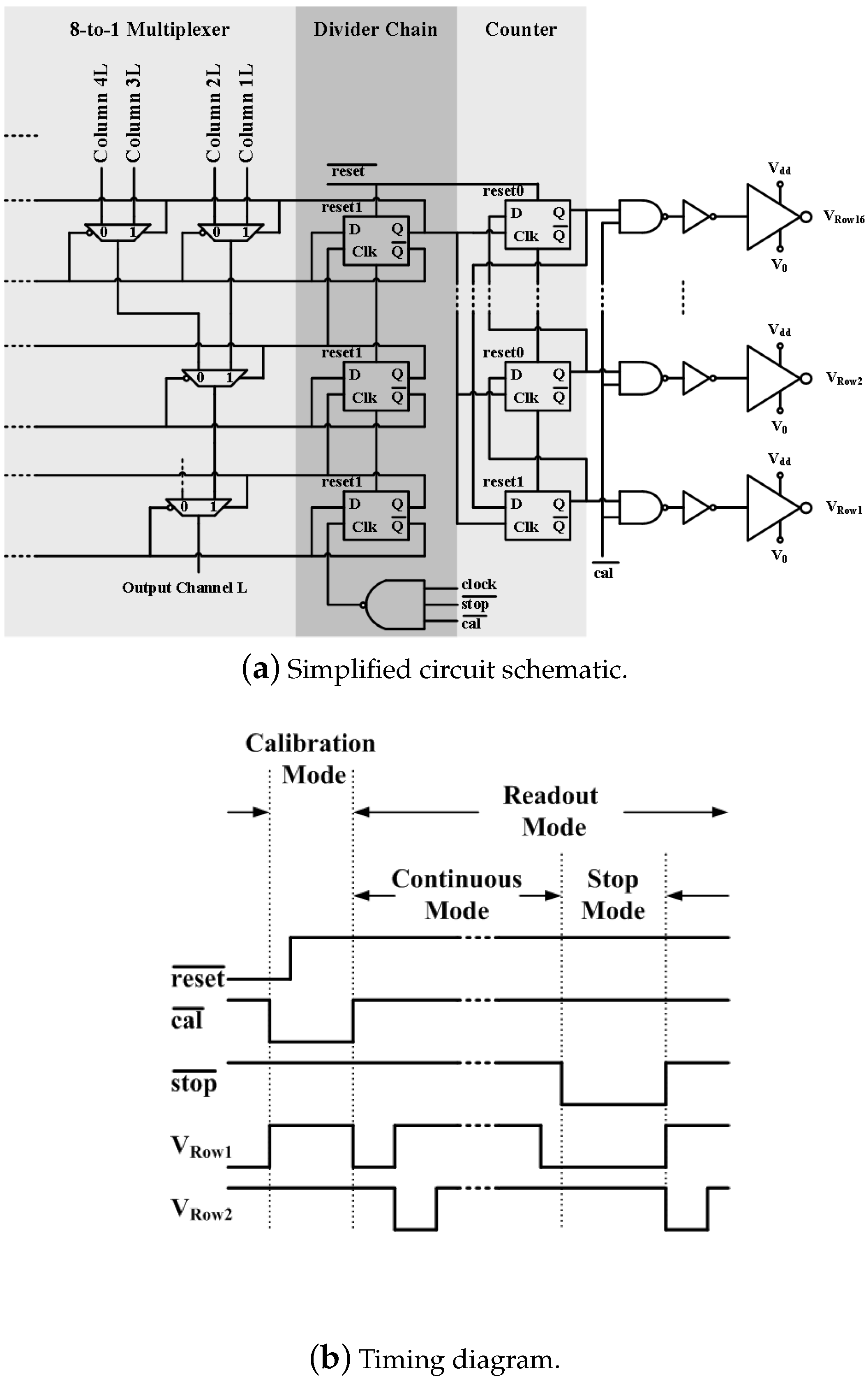
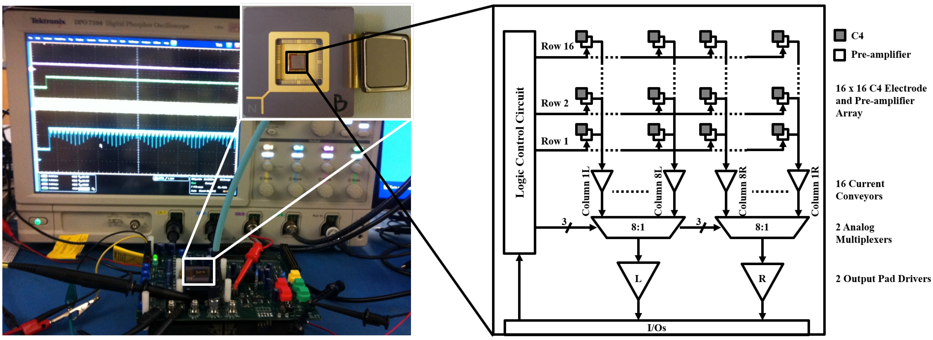
2.4. Time-Division Multiplexing and Chip Operation Modes

3. Fabrication and Packaging

4. Chip Characterization
4.1. Electrical Testing
4.1.1. System Voltage Gain
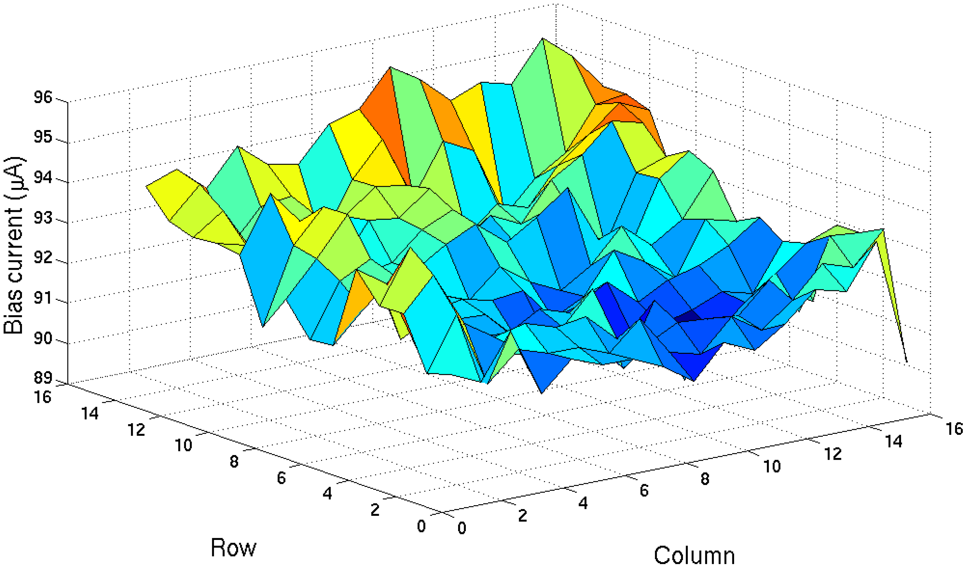
4.1.2. Process Variation
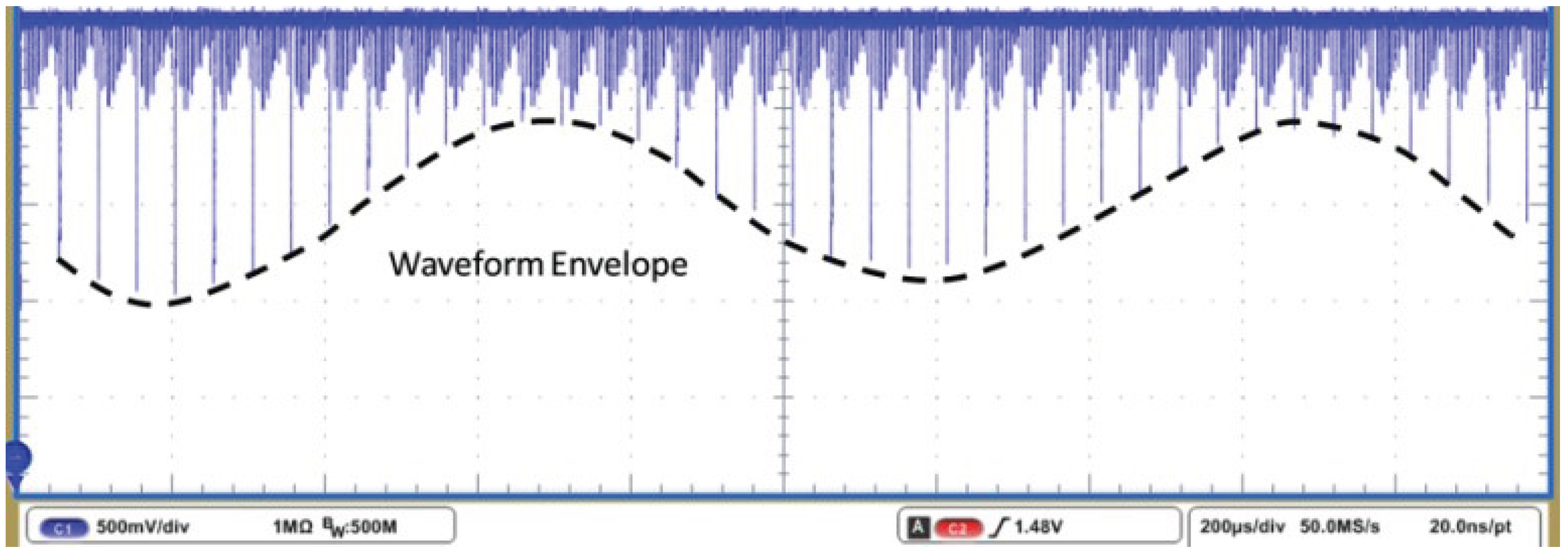
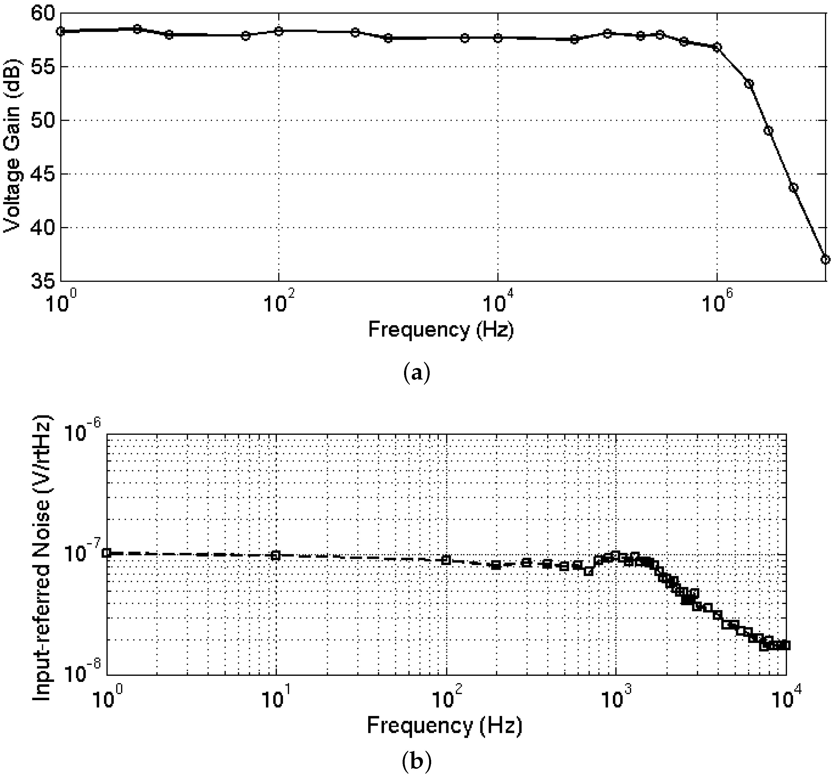
4.1.3. Frequency Response and Noise Performance
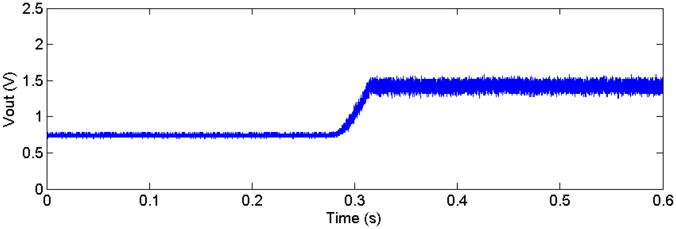
4.2. Electrical Testing With the In Vitro Package

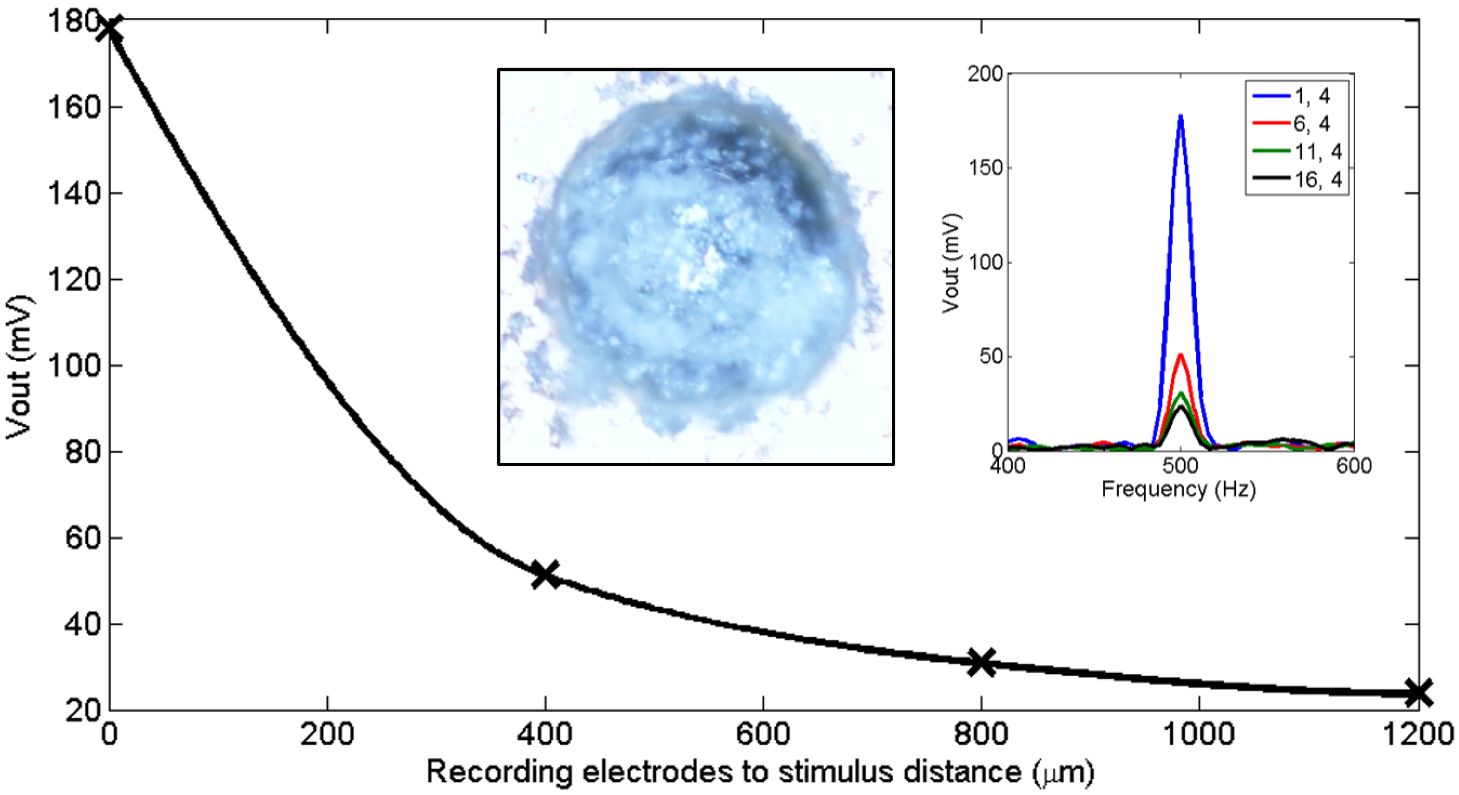
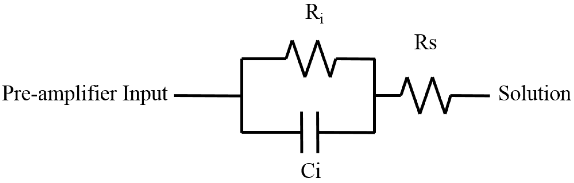
4.3. C4 Impedance Measurements
5. Acute Rat Cortical Recording
5.1. Surgical Procedure
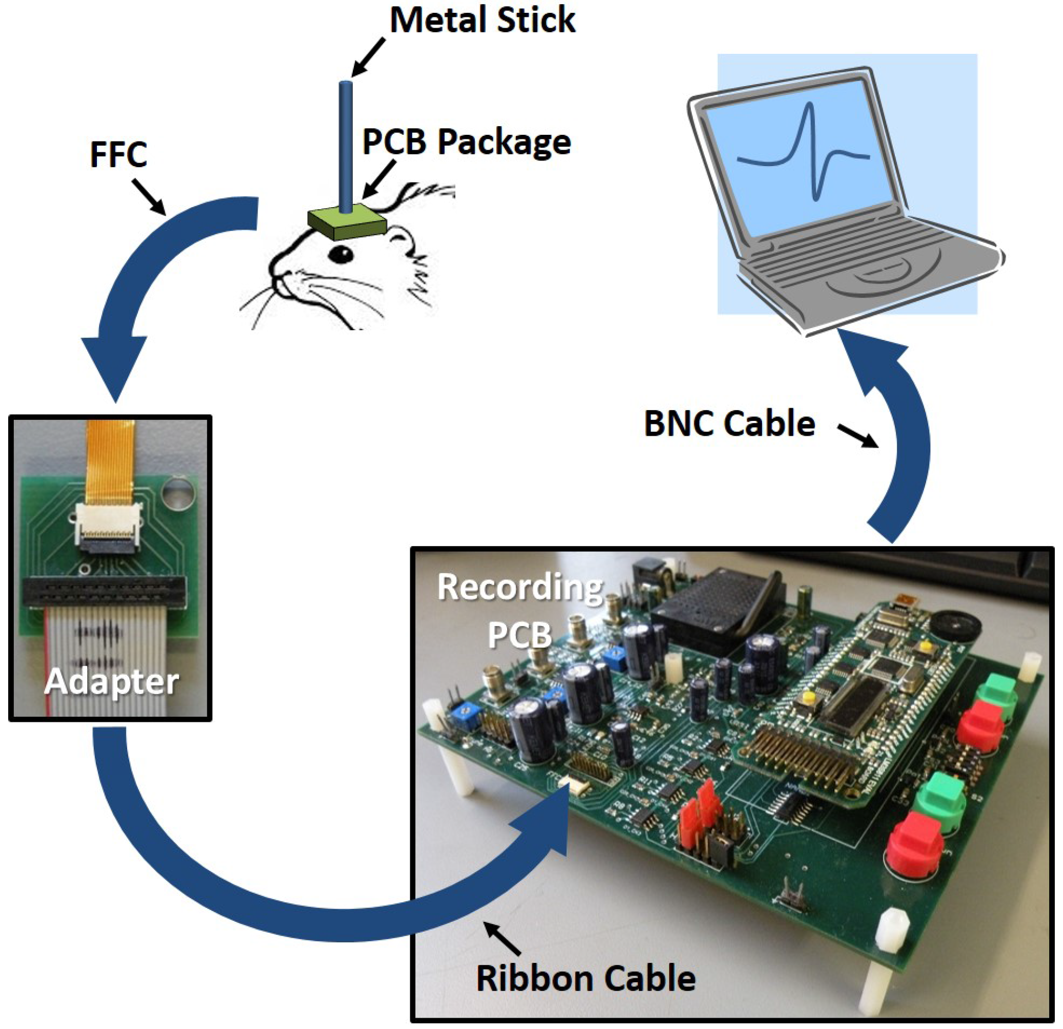
5.2. Recording Procedures
6. Discussion and Conclusions
7. Future Work
Acknowledgments
Author Contributions
Conflicts of Interest
References
- Hochberg, L.R.; Bacher, D.; Jarosiewicz, B.; Masse, N.Y.; Simeral, J.D.; Vogel, J.; Haddadin, S.; Liu, J.; Cash, S.S.; van der Smagt, P.; et al. Reach and grasp by people with tetraplegia using a neurally controlled robotic arm. Nature 2012, 485, 372–375. [Google Scholar] [CrossRef] [PubMed]
- Obien, M.; Deligkaris, K.; Bullmann, T.; Bakkum, D.; Frey, U. Revealing neuronal function through microelectrode array recordings. Front. Neurosci. 2015, 8. [Google Scholar] [CrossRef] [PubMed]
- Imfeld, K.; Garenne, A.; Martinoia, S.; Koudelka-Hep, M.; Berdondini, L. Motivations and APS-based solution for high-resolution extracellular recording from in-vitro neuronal networks. In Proceedings of the 3rd International IEEE/EMBS Conference on Neural Engineering, Kohala Coast, HI, USA, 2–5 May 2007; pp. 225–228.
- Prasad, A.; Sahin, M. Can motor volition be extracted from the spinal cord? J. NeuroEng. Rehabil. 2012, 9, 372–375. [Google Scholar] [CrossRef] [PubMed]
- Ordek, G.; Groth, J.D.; Sahin, M. Differential effects of ketamine/xylazine anesthesia on the cerebral and cerebellar cortical activities in the rat. J. Neurophysi. 2013, 109, 1435–1443. [Google Scholar] [CrossRef] [PubMed]
- Engel, A.K.; Moll, C.K.E.; Fried, I.; Ojemann, G.A. Invasive recordings from the human brain: Clinical insights and beyond. Nature Rev. Neurosci. 2005, 6, 35–47. [Google Scholar] [CrossRef] [PubMed]
- Buzsaki, G.; Anastassiou, C.A.; Koch, C. The origin of extracellular fields and currents—EEG, ECoG, LFP and spikes. Nature Rev. Neurosci. 2012, 13, 407–420. [Google Scholar] [CrossRef] [PubMed]
- Shulyzki, R.; Abdelhalim, K.; Bagheri, A.; Salam, M.; Florez, C.; Velazquez, J.; Carlen, P.; Genov, R. 320-Channel Active Probe for High-Resolution Neuromonitoring and Responsive Neurostimulation. IEEE Trans. Biomed. Circuits Syst. 2014, 9, 34–49. [Google Scholar] [CrossRef] [PubMed]
- Harrison, R.R. The design of integrated circuits to observe brain activity. IEEE Proc. 2008, 96, 1213–1216. [Google Scholar] [CrossRef]
- Eversmann, B.; Jenkner, M.; Hofmann, F.; Paulus, C.; Brederlow, R.; Holzapfl, B.; Fromherz, P.; Merz, M.; Brenner, M.; Schreiter, M.; et al. A 128 × 128 CMOS biosensor array for extracellular recording of neural activity. IEEE J. Solid State Circuits 2003, 38, 2306–2317. [Google Scholar] [CrossRef]
- Frey, U.; Heer, F.; Pedron, R.; Hafizovic, S.; Greve, F.; Sedivy, J.; Kirstein, K.; Hierlemann, A. An 11k-electrode 126-channel high-density microelectrode array to interact with electrogenic cells. In Proceedings of the IEEE International Solid-State Circuits Conference (ISSCC’07), San Francisco, CA, USA, 11–15 February 2007; pp. 158–159.
- Imfeld, K.; Neukom, S.; Maccione, A.; Bornat, Y.; Martinoia, S.; Farine, P.A.; Koudelka-Hep, M.; Berdondini, L. Large-scale, high-resolution data acquisition system for extracellular recording of electrophysiological activity. IEEE Trans. Biomed. Eng. 2008, 55, 2064–2073. [Google Scholar] [CrossRef] [PubMed]
- Nordhausen, C.T.; Maynard, E.M.; Normann, R.A. Single unit recording capabilities of a 100-microelectrode array. Brain Res. 1996, 726, 129–140. [Google Scholar] [CrossRef]
- Frieswijk, T.A.; Bielen, J.A.; Rutten, W.L.C.; Bergveld, P. Development of a solder bump technique for contacting a three-dimensional multi electrode array. Microsyst. Technol. 1997, 3, 48–52. [Google Scholar] [CrossRef]
- Aziz, J.N.Y.; Abdelhalim, K.; Shulyzki, R.; Genov, R.; Bardakjian, B.L.; Derchansky, M.; Serletis, D.; Carlen, P.L. 256-channel neural recording and delta compression microsystem with 3D electrodes. IEEE J. Solid State Circuits 2009, 44, 995–1005. [Google Scholar] [CrossRef]
- Song, Y.K.; Borton, D.; Park, S.; Patterson, W.; Bull, C.; Laiwalla, F.; Mislow, J.; Simeral, J.; Donoghue, J.; Nurmikko, A. Active Microelectronic Neurosensor Arrays for Implantable Brain Communication Interfaces. IEEE Trans. Neural Syst. Rehabil. Eng. 2009, 17, 339–345. [Google Scholar] [CrossRef] [PubMed]
- Gao, H.; Walker, R.; Nuyujukian, P.; Makinwa, K.; Shenoy, K.; Murmann, B.; Meng, T. HermesE: A 96-Channel Full Data Rate Direct Neural Interface in 0.13 μm CMOS. IEEE J. Solid State Circuits 2012, 47, 1043–1055. [Google Scholar] [CrossRef]
- Sodagar, A.M.; Perlin, G.E.; Yao, Y.; Najafi, K.; Wise, K.D. An implantable 64-channel wireless microsystem for single-unit neural recording. IEEE J. Solid State Circuits 2009, 44, 2591–2604. [Google Scholar] [CrossRef]
- Bagheri, A.; Gabran, S.; Salam, M.; Perez Velazquez, J.; Mansour, R.; Salama, M.; Genov, R. Massively-Parallel Neuromonitoring and Neurostimulation Rodent Headset With Nanotextured Flexible Microelectrodes. IEEE Trans. Biomed. Circuits Syst. 2013, 7, 601–609. [Google Scholar] [CrossRef] [PubMed]
- Gabran, S.; Salam, M.; Dian, J.; El-Hayek, Y.; Velazquez, J.; Genov, R.; Carlen, P.; Salama, M.; Mansour, R. High-Density Intracortical Microelectrode Arrays With Multiple Metallization Layers for Fine-Resolution Neuromonitoring and Neurostimulation. IEEE Trans. Neural Syst. Rehabil. Eng. 2013, 21, 869–879. [Google Scholar] [CrossRef] [PubMed]
- Lopez, C.; Andrei, A.; Mitra, S.; Welkenhuysen, M.; Eberle, W.; Bartic, C.; Puers, R.; Yazicioglu, R.; Gielen, G. An Implantable 455-Active-Electrode 52-Channel CMOS Neural Probe. IEEE J. Solid State Circuits 2014, 49, 248–261. [Google Scholar] [CrossRef]
- Harrison, R.R.; Charles, C. A low-power low-noise CMOS amplifier for neural recording applications. IEEE J. Solid State Circuits 2003, 38, 958–965. [Google Scholar] [CrossRef]
- Yun, X.; Kim, D.; Stanaćević, M.; Mainen, Z. Low-Power High-Resolution 32-channel Neural Recording System. In Proceedings of the 29th Annual International Conference of the IEEE Engineering in Medicine and Biology Society (EMBC’07), Lyon, France, 22–26 August 2007; pp. 2373–2376.
- Wattanapanitch, W.; Sarpeshkar, R. A Low-Power 32-Channel Digitally Programmable Neural Recording Integrated Circuit. IEEE Trans. Biomed. Circuits Syst. 2011, 5, 592–602. [Google Scholar] [CrossRef] [PubMed]
- Han, D.; Zheng, Y.; Rajkumar, R.; Dawe, G.; Je, M. A 0.45 V 100-Channel Neural-Recording IC With Sub-μW/Channel Consumption in 0.18 μm CMOS. In Proceedings of the 2013 IEEE International Solid-State Circuits Conference Digest of Technical Papers (ISSCC), San Francisco, CA, USA, 17–21 February 2013; Volume 7, pp. 735–746.
- Wright, S.; Polastre, R.; Gan, H.; Buchwalter, L.; Horton, R.; Andry, P.; Sprogis, E.; Patel, C.; Tsang, C.; Knickerbocker, J.; et al. Characterization of micro-bump C4 interconnects for Si-carrier SOP applications. In Proceedings of the 56th Electronic Components and Technology Conference, San Diego, CA, USA, 30 May–2 June 2006; pp. 633–640.
- Wen, S.; Park, K.; Thompson, P.; Shirley, D.; Lee, J.; Park, H. Flip chip assembly with advanced RDL technology. In Proceedings of the 2013 14th International Conference on Electronic Packaging Technology (ICEPT), Dalian, China, 11–14 August 2013; pp. 57–59.
- Frank, W.; Schenker, I.; Schmutz, P.; Hierlemann, A. Impedance Characterization and Modeling of Electrodes for Biomedical Applications. IEEE Trans. Biomed. Eng. 2005, 52, 1295–1302. [Google Scholar] [CrossRef] [PubMed]
- Joye, N.; Schmid, A.; Leblebici, Y. Electrical Modeling of the Cell-Electrode Interface for Recording Neural Activity from High-Density Microelectrode Arrays. Neurocomput. Elsevier 2009, 73, 250–259. [Google Scholar] [CrossRef]
- Higuera, A. Neural Interface Model for a Pt/Au C4 Bump Microelectrode Array. Unpublished work. 2016. [Google Scholar]
- Wang, L.; Freedman, D.S.; Knepper, R.W.; Ünlü, M.S.; Sahin, M. A 16 × 16 Multi-electrode Array with Integrated CMOS Amplifiers for Neural Signal Recording. In Proceedings of the 2011 IEEE Biomedical Circuits and Systems Conference (BioCAS), San Diego, CA, USA, 10–12 November 2011; pp. 82–85.
- Carusone, T.C.; Johns, D.A.; Martin, K.W. Analog Integrated Circuit Design, 2nd ed.; John Wiley & Sons: Hoboken, NJ, USA, 2011. [Google Scholar]
- Majidzadeh, V.; Schmid, A.; Leblebici, Y. A 16-channel 220 μW neural recording IC with embedded delta compression. In Proceedings of the 2011 IEEE Biomedical Circuits and Systems Conference (BioCAS), San Diego, CA, USA, 10–12 November 2011; pp. 9–12.
- Hosseini-Nejad, H.; Jannesari, A.; Sodagar, A. Data Compression in Brain-Machine/Computer Interfaces Based on the Walsh-Hadamard Transform. IEEE Trans. Biomed. Circuits Syst. 2014, 8, 129–137. [Google Scholar] [CrossRef] [PubMed]
- Yazdani, N.; Rashidi, A.; Sodagar, A.M.; Mohebbi, M. Reduction of spatial data redundancy in implantable multi-channel neural recording microsystems. In Proceedings of the 2014 IEEE Biomedical Circuits and Systems Conference (BioCAS), Lausanne, Switzerland, 22–24 October 2014; pp. 208–211.
- Berdondini, L.; Wal, P.D.V.D.; Rooij, N.F.D.; Koudelka-Hep, M. Development of an electroless post-processing technique for depositing gold as electrode material on CMOS devices. Sens. Actuators B Chem. 2004, 99, 505–510. [Google Scholar] [CrossRef]
- Aziz, J.N.Y.; Genov, R.; Bardakjian, B.L.; Derchansky, M.; Carlen, P.L. Brain-silicon interface for high-resolution in vitro neural recording. IEEE Trans. Biomed. Circuits Syst. 2007, 1, 56–62. [Google Scholar] [CrossRef] [PubMed]
- Graham, A.H.D.; Bowen, C.R.; Surguy, S.M.; Robbins, J.; Taylor, J. New prototype assembly methods for biosensor integrated circuits. Med. Eng. Phys. 2011, 33, 973–979. [Google Scholar] [CrossRef] [PubMed]
© 2016 by the authors; licensee MDPI, Basel, Switzerland. This article is an open access article distributed under the terms and conditions of the Creative Commons by Attribution (CC-BY) license (http://creativecommons.org/licenses/by/4.0/).
Share and Cite
Wang, L.; Freedman, D.; Sahin, M.; Ünlü, M.S.; Knepper, R. Active C4 Electrodes for Local Field Potential Recording Applications. Sensors 2016, 16, 198. https://doi.org/10.3390/s16020198
Wang L, Freedman D, Sahin M, Ünlü MS, Knepper R. Active C4 Electrodes for Local Field Potential Recording Applications. Sensors. 2016; 16(2):198. https://doi.org/10.3390/s16020198
Chicago/Turabian StyleWang, Lu, David Freedman, Mesut Sahin, M. Selim Ünlü, and Ronald Knepper. 2016. "Active C4 Electrodes for Local Field Potential Recording Applications" Sensors 16, no. 2: 198. https://doi.org/10.3390/s16020198