
Fabrication of Capacitive Acoustic Resonators Combining 3D Printing and 2D Inkjet Printing Techniques

Abstract
:
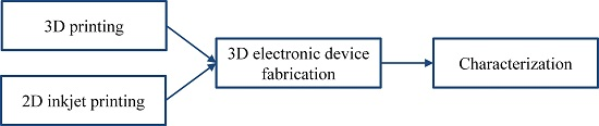
1. Introduction

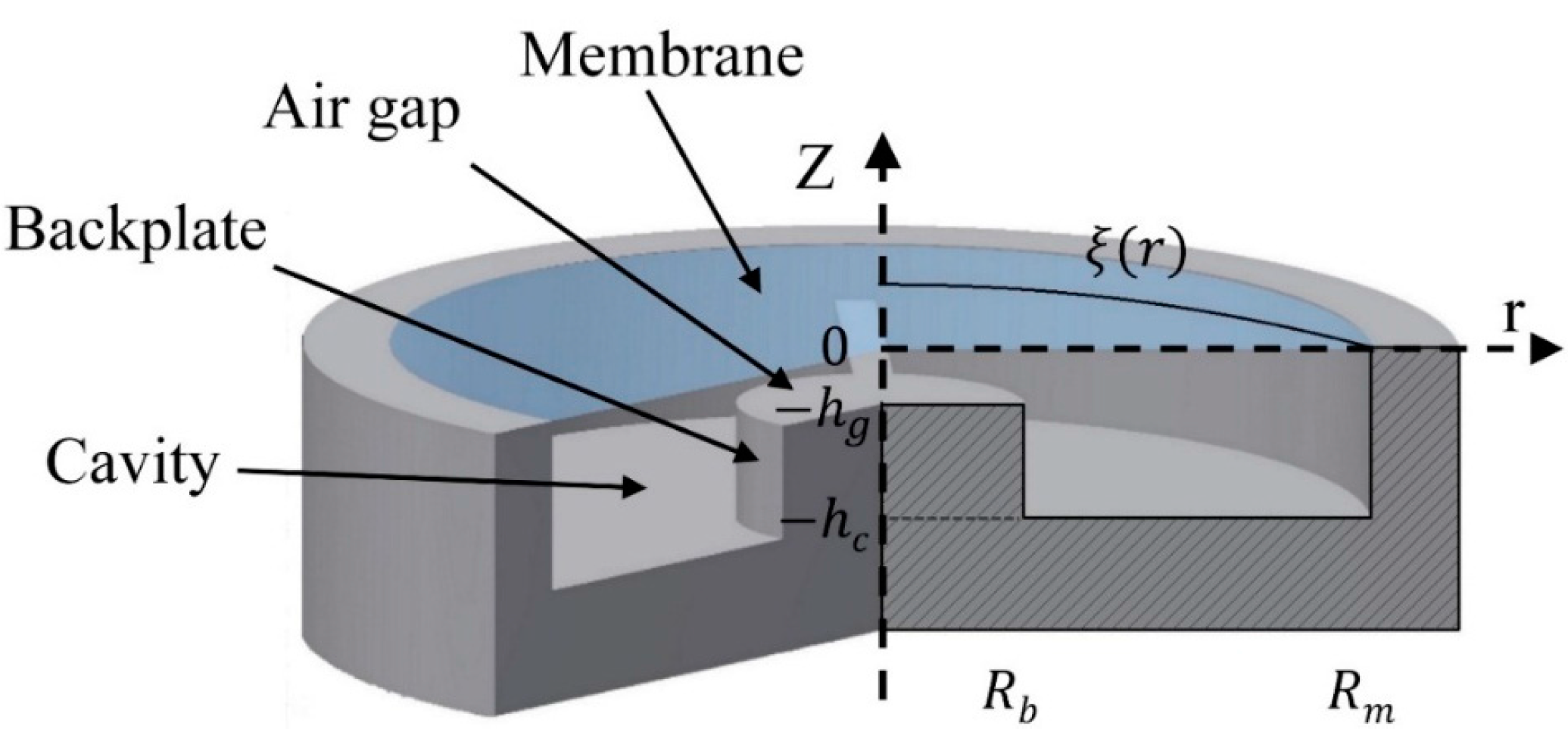
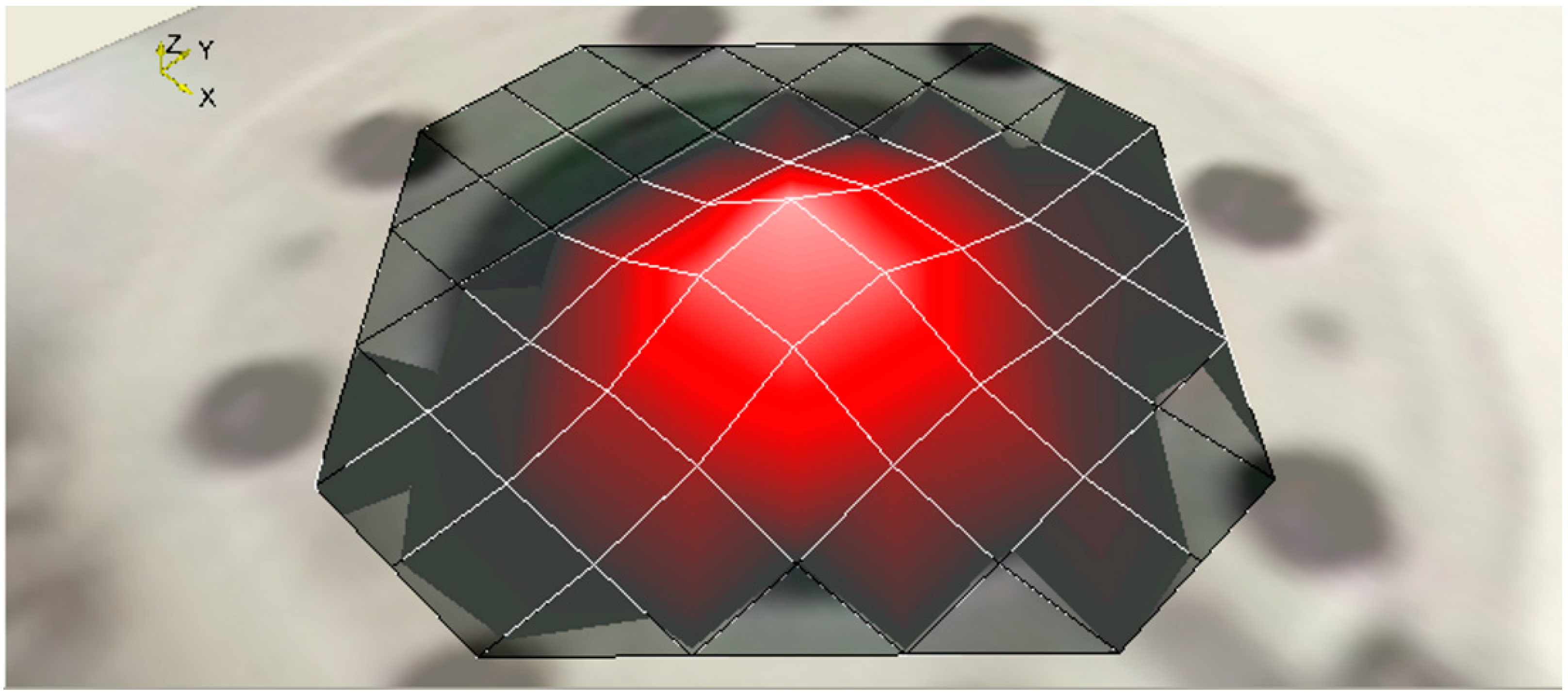
2. Acoustic Transducer Design
3. Experimental Details
3.1. Materials and Printing Systems
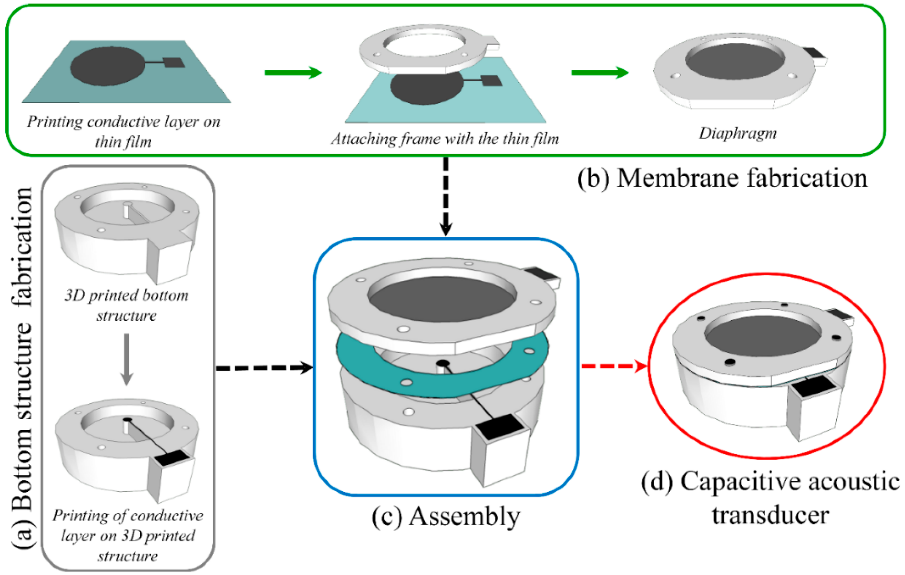
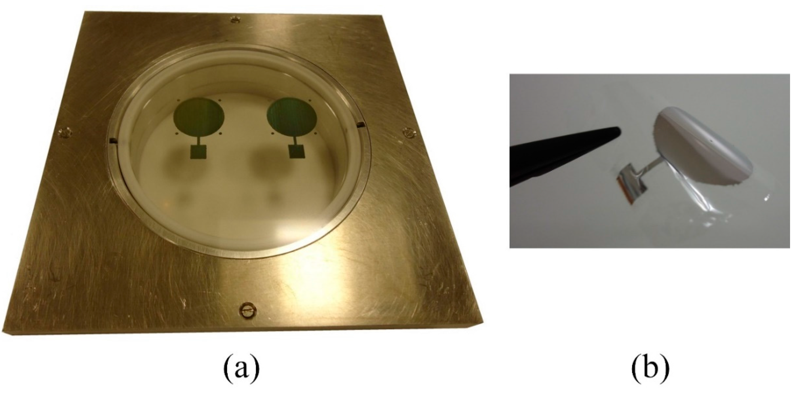
3.2. Device Fabrication


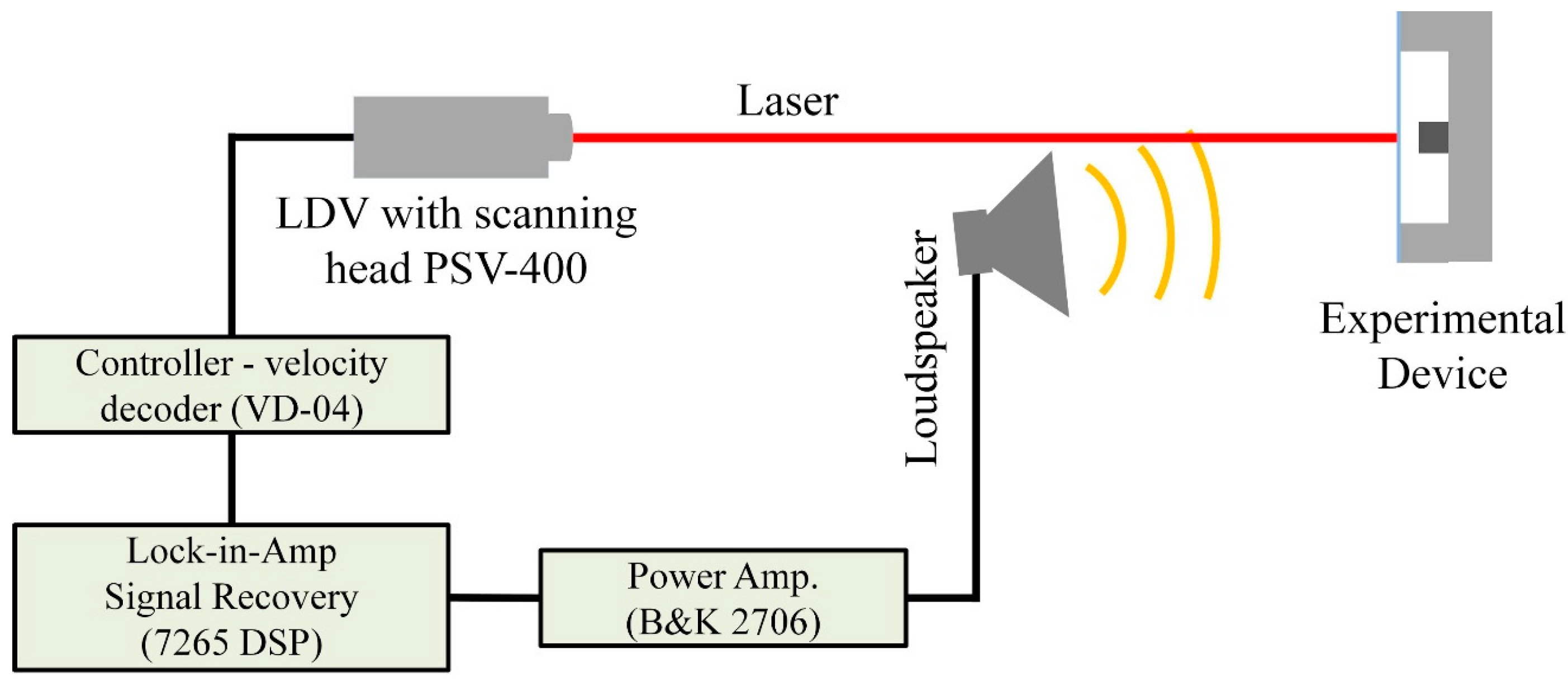
3.3. Experimental Procedure
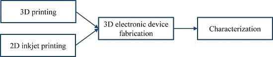
4. Result and Discussion
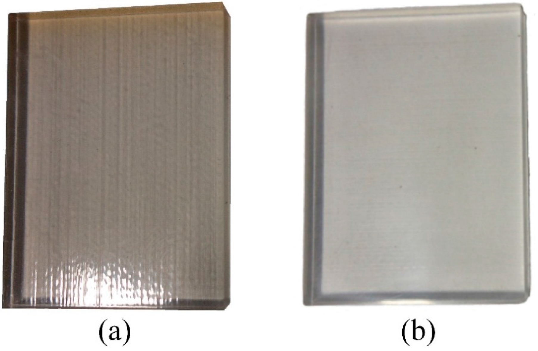
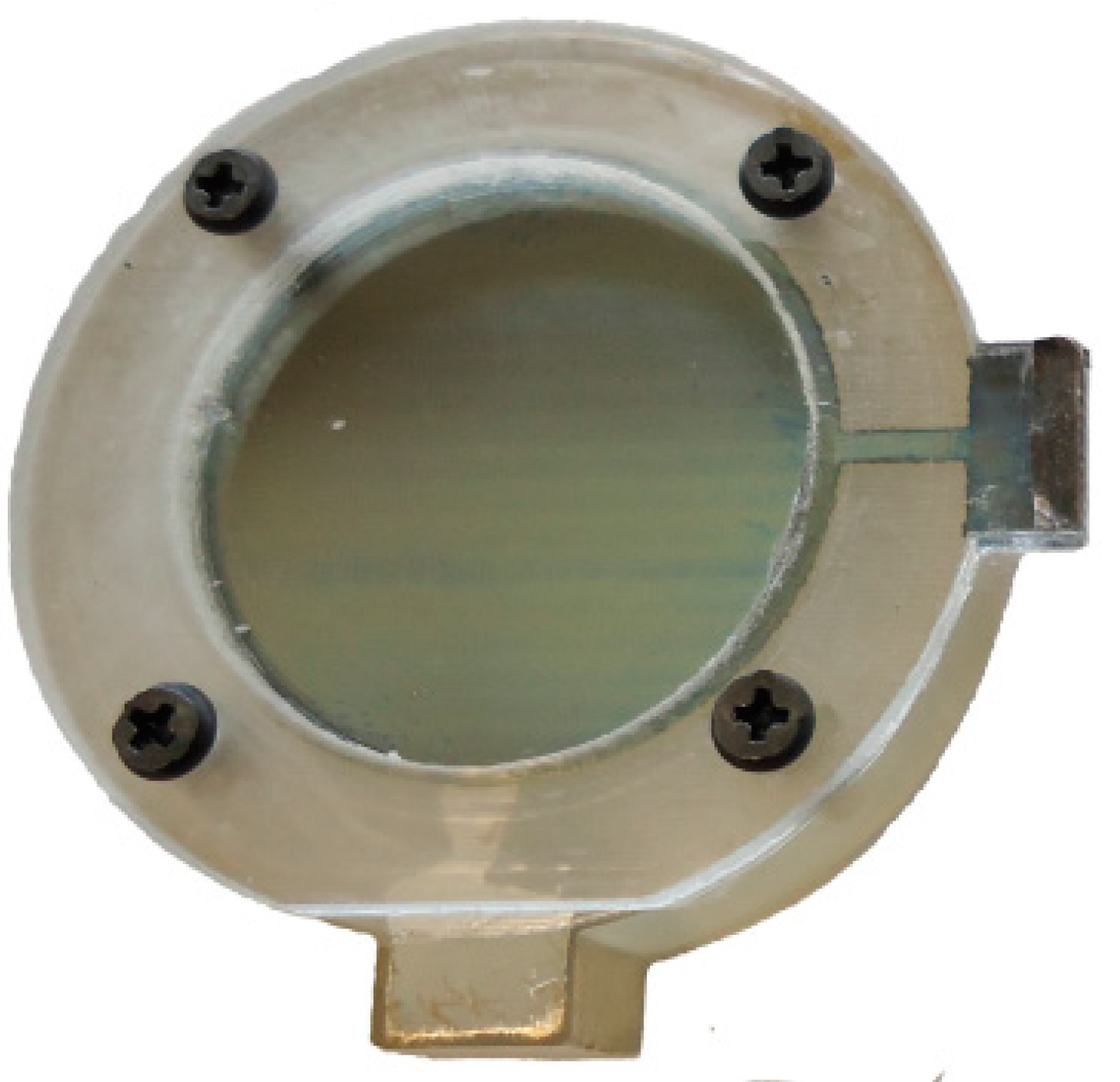
4.1. Three-Dimensional (3D) Printed Structure
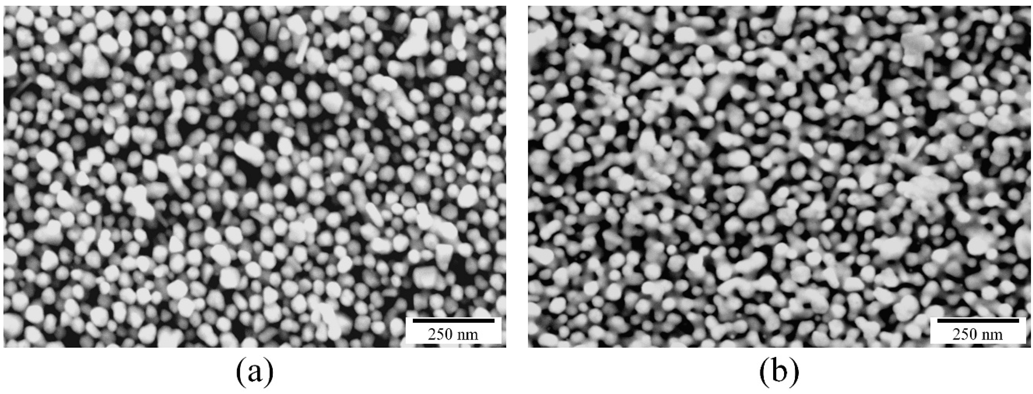
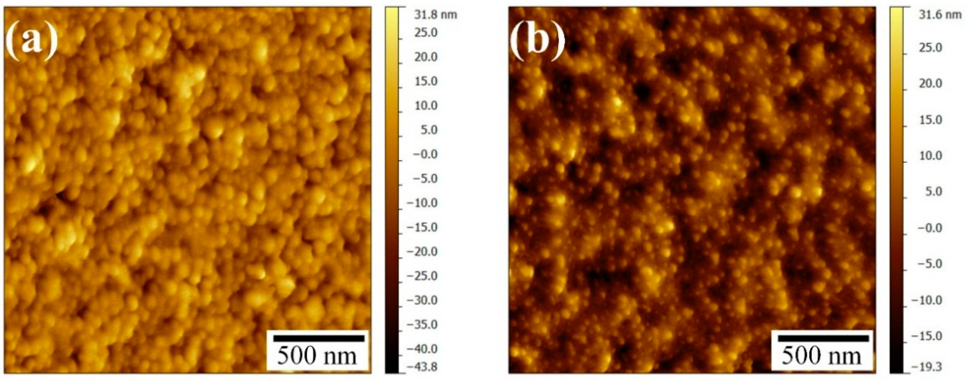
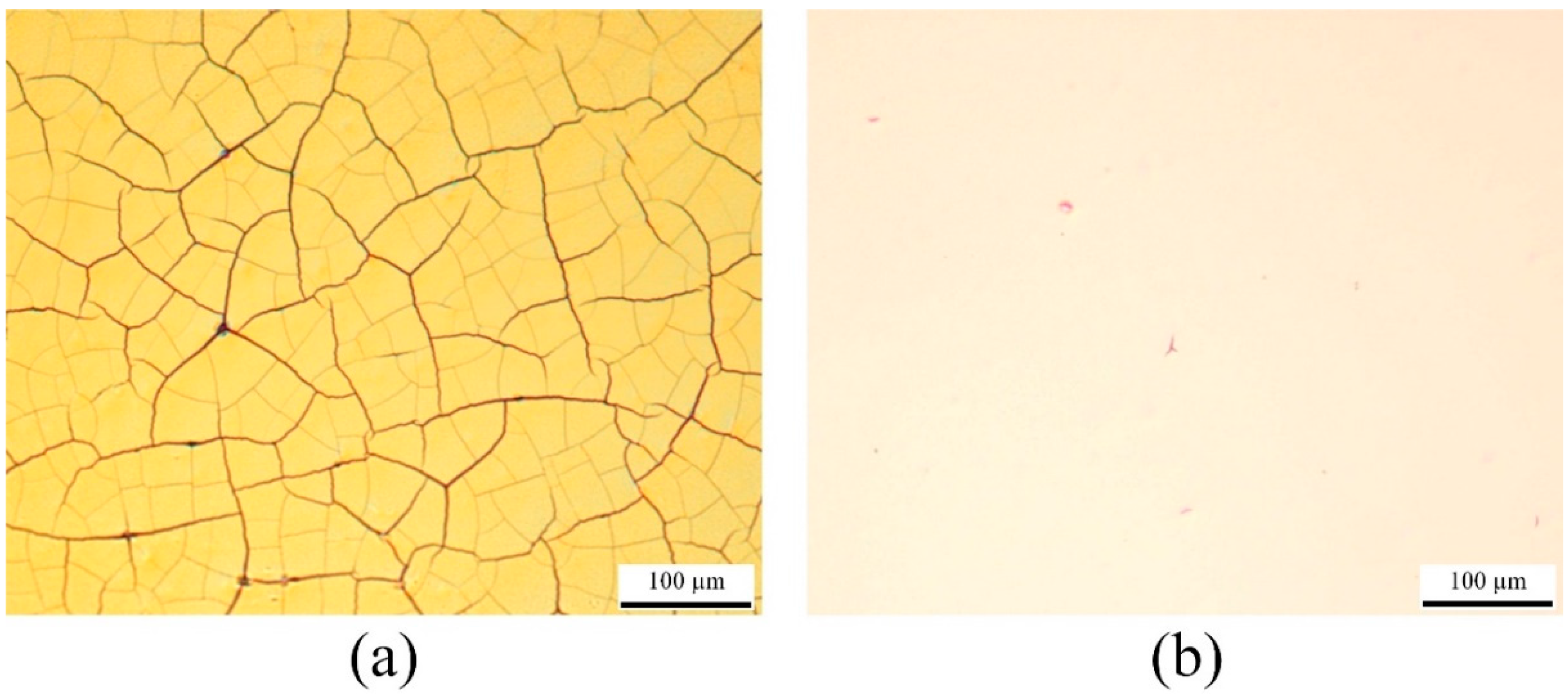
4.2. Characterization of Printed Layer on 3D Printed Substrate


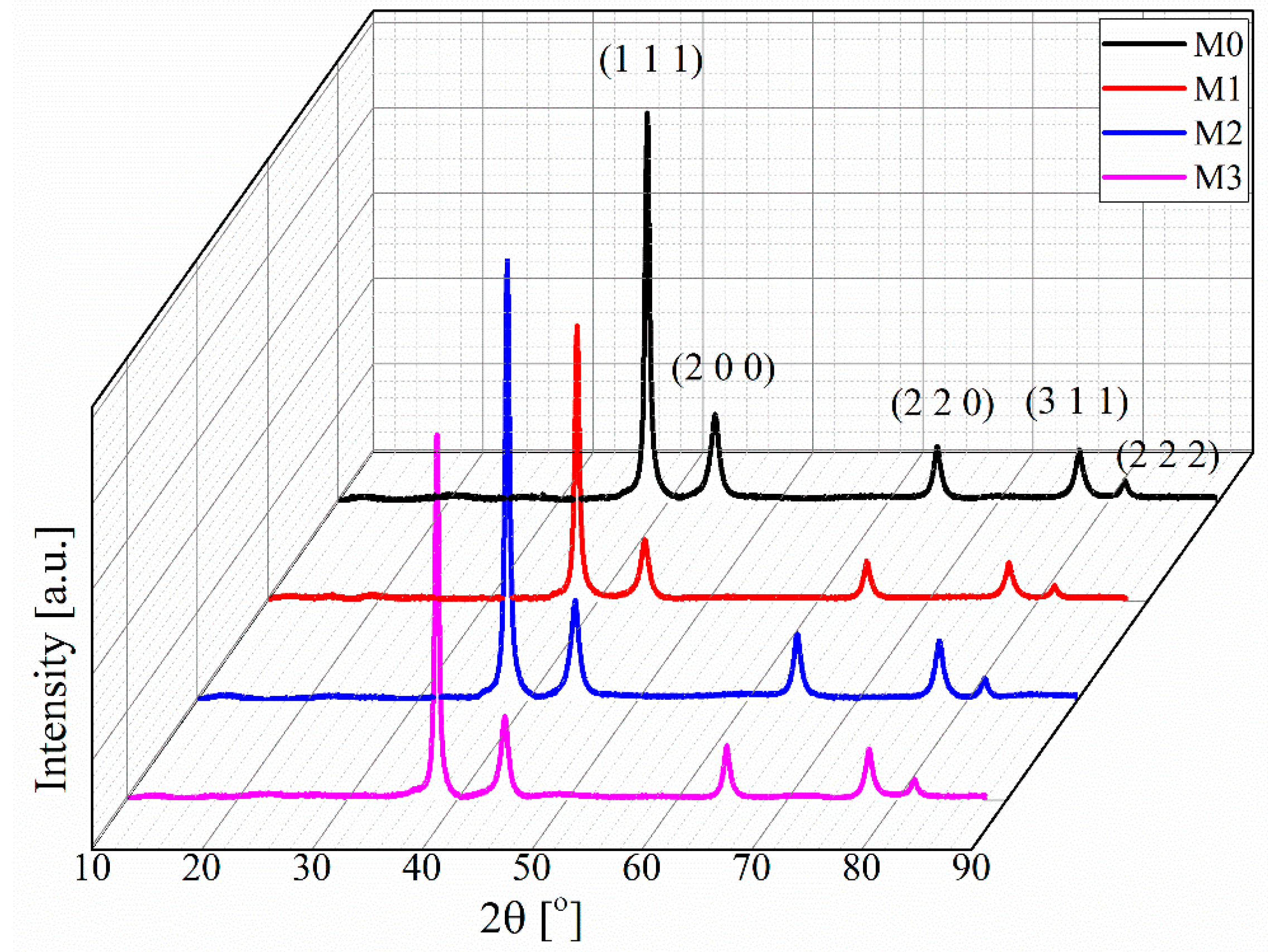
| Sample Code | Photonic Sintering Parameters | Average Grain Size D | |||
|---|---|---|---|---|---|
| VB | Ton | Toff | Np | ||
| V | µs | µs | nm | ||
| M0 | - | - | - | - | 51.6 ± 1.3 |
| M1 | 400 | 15 | 1000 | 15 | 58.6 ± 0.5 |
| M2 | 400 | 15 | 1000 | 25 | 67.7 ± 2.5 |
| M3 | 400 | 15 | 1000 | 40 | 87.2 ± 4.1 |
| Sample Code | Photonic Sintering Parameters | Roughness | ||||
|---|---|---|---|---|---|---|
| VB | Ton | Toff | Np | Sa | Sq | |
| V | µs | µs | nm | nm | ||
| M0 | - | - | - | - | 7.1 ± 0.9 | 9.2 ± 1.3 |
| M1 | 400 | 15 | 1000 | 15 | 6.4 ± 0.6 | 8.2 ± 0.7 |
| M2 | 400 | 15 | 1000 | 25 | 7.5 ± 0.5 | 10.3 ± 1.3 |
| M3 | 400 | 15 | 1000 | 40 | 6.0 ± 0.5 | 7.7 ± 0.7 |
| Sa → Arithmetic mean of roughness | Sq → Root mean square of roughness | |||||

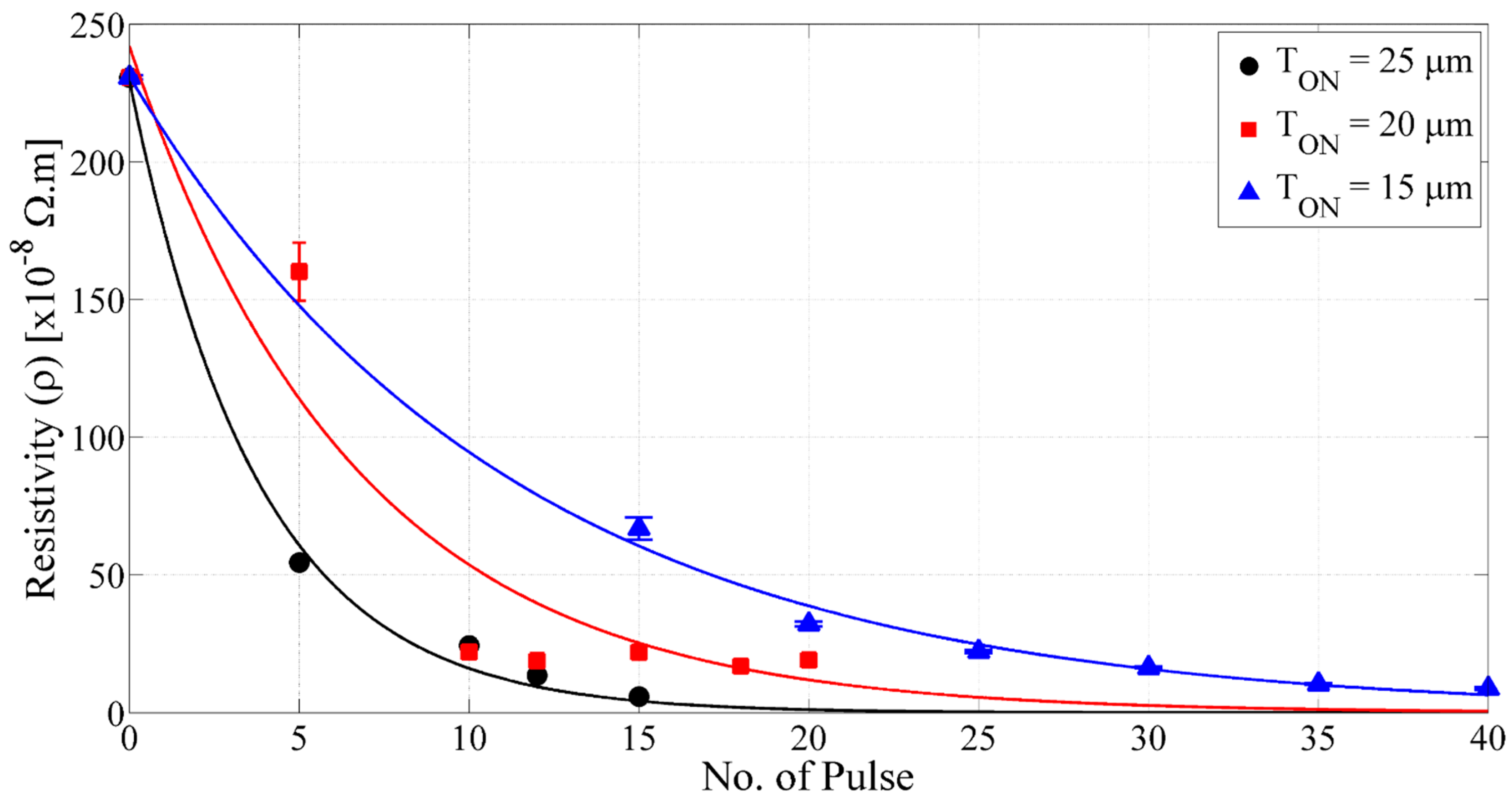
4.3. Conductive Layer Printed on Thin Film


| Sintering Parameters | Conductivity | Grain Size | |
|---|---|---|---|
| Temperature | Time | ||
| °C | min | S·m−1 | nm |
| 90 | 30 | 1.6 × 10⁶ | 42.9 ± 0.8 |
| 120 | 30 | 3.3 × 10⁶ | 45.3 ± 1.3 |
| 140 | 30 | 5.5 × 10⁶ | 51.3 ± 1.5 |
| 140 | 10 | 5.1 × 10⁶ | 48.1 ± 1.3 |
| 140 | 60 | 7.2 × 10⁶ | 54.6 ± 2.2 |
4.4. Characterization of the Capacitive Acoustic Transducer
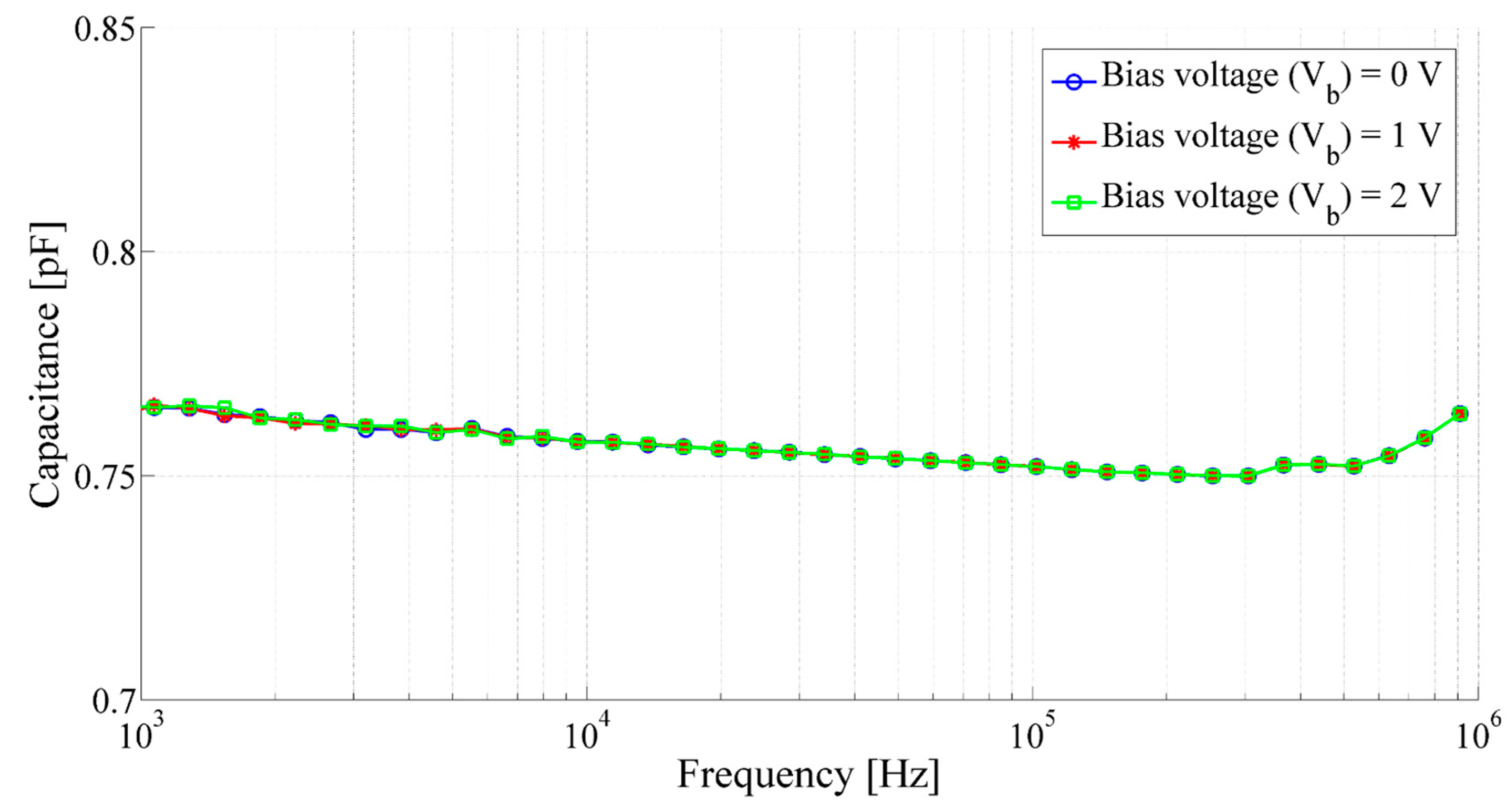
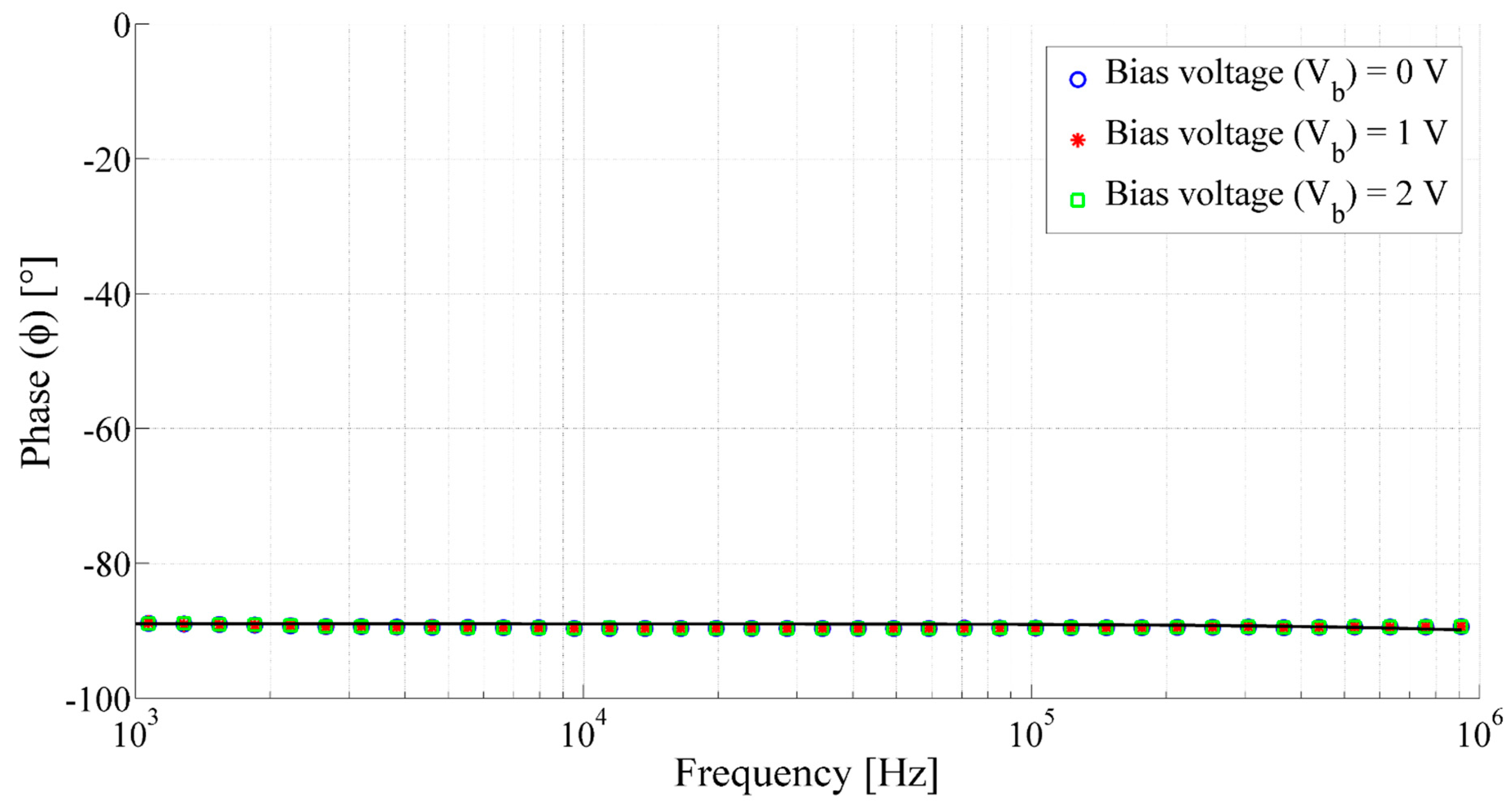
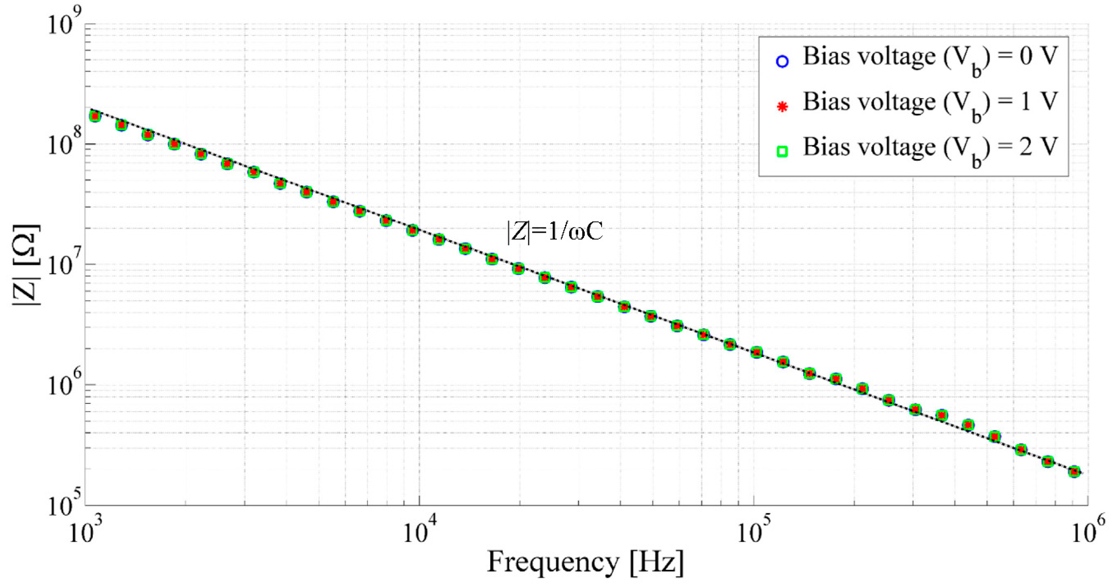
4.4.1. Static Capacitance Measurement


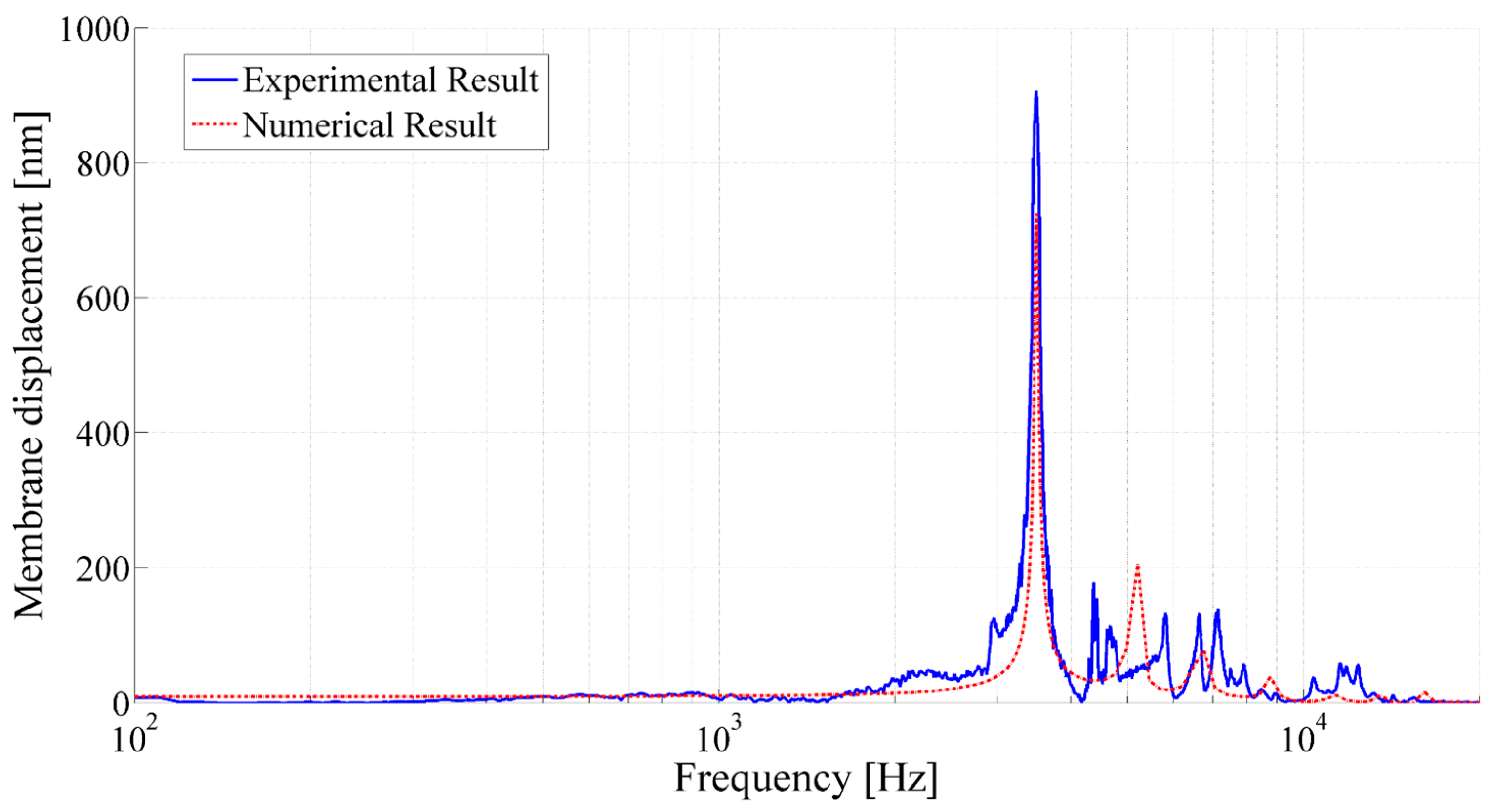
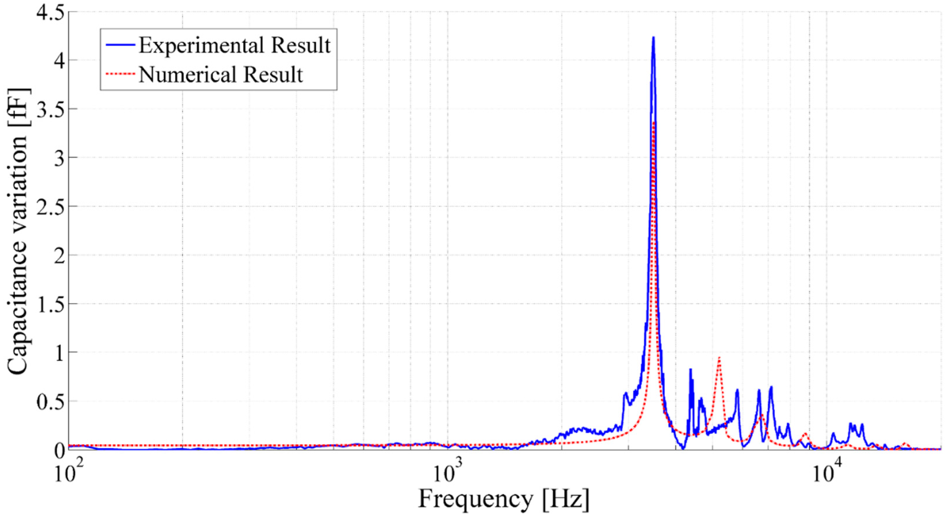
4.4.2. Dynamic Characterization
| Device Parameters | Numerical Results | Experimental Results | |||||||
|---|---|---|---|---|---|---|---|---|---|
| Rm | RB | hc | hg | Tm | tm | f10 | Qf | f10 | Qf |
| mm | mm | mm | µm | N/m | µm | Hz | Hz | ||
| 8.1 | 0.87 | 3990 | 67.7 | 48 | 23 | 3489.2 | 61.6 | 3490 | 34 |


5. Conclusions
Supplementary Files
Supplementary File 1Acknowledgments
Author Contributions
Conflicts of Interest
References
- Scheeper, P.R.; van der Donk, A.G.H.; Olthuis, W.; Bergveld, P. A Review of Silicon Microphones. Sens. Actuators Phys. 1994, 44, 1–11. [Google Scholar] [CrossRef]
- Spinnaker. “SPINNAKER”. Spinnaker. 2012. Available online: http://www.spinnaker-rfid.com/ (accessed on 16 June 2015).
- Podkovskiy, A.; Honzík, P.; Durand, S.; Joly, N.; Bruneau, M. Miniaturized Electrostatic Receiver with Small-Sized Backing Electrode. In Proceedings of the Meetings on Acoustics, Montreal, QC, Canada, 2–7 June 2013; Volume 19, p. 030047.
- Honzík, P.; Podkovskiy, A.; Durand, S.; Joly, N.; Bruneau, M. Analytical and Numerical Modeling of an Axisymmetrical Electrostatic Transducer with Interior Geometrical Discontinuity. J. Acoust. Soc. Am. 2013, 134, 3573–3579. [Google Scholar] [CrossRef] [PubMed]
- Haque, R.I.; Loussert, C.; Sergent, M.; Benaben, P.; Boddaert, X. Optimization of Capacitive Acoustic Resonant Sensor Using Numerical Simulation and Design of Experiment. Sensors 2015, 15, 8945–8967. [Google Scholar] [CrossRef] [PubMed] [Green Version]
- Mitchell, A.W.; Ning, Y.B.; Tait, N.R. Fabrication of a Surface Micromachined Capacitive Microphone using a Dry-Etch Process. US 5573679 A, 12 November 1996. [Google Scholar]
- Kamyshny, A.; Steinke, J.; Magdassi, S. Metal-based Inkjet Inks for Printed Electronics. Open Appl. Phys. J. 2011, 4, 19–36. [Google Scholar] [CrossRef]
- De Cesare, G.; Gavesi, M.; Palma, F.; Ricco, B. A Novel a-Si: H Mechanical Stress Sensor. Thin Solid Films 2003, 427, 191–195. [Google Scholar] [CrossRef]
- Olmi, G. Investigation on the Influence of Temperature Variation on the Response of Miniaturised Piezoresistive Sensors. Strain 2009, 45, 63–76. [Google Scholar] [CrossRef]
- Peiner, E.; Tibrewala, A.; Bandorf, R.; Biehl, S.; Lüthje, H.; Doering, L. Micro Force Sensor with Piezoresistive Amorphous Carbon Strain Gauge. Sens. Actuators Phys. 2006, 130–131, 75–82. [Google Scholar] [CrossRef]
- Alpuim, P.; Chu, V.; Conde, J.P. Piezoresistive Sensors on Plastic Substrates Using Doped Microcrystalline Silicon. IEEE Sens. J. 2002, 2, 336–341. [Google Scholar] [CrossRef]
- Creighton, J.R.; Ho, P. Introduction to Chemical Vapor Deposition (CVD). In Chemical Vapor Deposition; Park, J.H., Sudarshan, T.S., Eds.; ASM International: Materials Park, OH, USA, 2001; Volume 2, pp. 1–22. [Google Scholar]
- Blayo, A.; Pineaux, B. Printing Processes and Their Potential for RFID Printing. In Proceedings of the Joint sOc-EUSAI Conference, Grenoble, France, 12–14 October 2005; pp. 27–30.
- Bliss, A. Printed Electronics: The Future at Your Fingertips. May 2013. Available online: http://www.computerarts.co.uk/blog/printed-electronics-future-your-fingertips-133664 (accessed on 14 December 2014).
- Acreo Swedish ICT. Printed Electronics. Available online: https://www.acreo.se/expertise/printed-electronics (accessed on 26 June 2015).
- Thin Film Electronics ASA. Thinfilm Receives First Order for Brand Protection Solution. Thinfilm: Memory Everywhere. 2013. Available online: http://www.thinfilm.no/news/thinfilm-receives-first-order-for-brand-protection-system/ (accessed on 26 June 2015).
- Li, Y.; Lu, D.; Wong, C.P. Electrical Conductive Adhesives with Nanotechnologies; Springer: New York, NY, USA, 2009. [Google Scholar]
- Wondmagegn, W.T.; Satyala, N.T.; Stiegler, H.J.; Quevedo-Lopez, M.A.; Forsythe, E.W.; Pieper, R.J.; Gnade, B.E. Simulation Based Performance Comparison of Transistors Designed Using Standard Photolithographic and Coarse Printing Design Specifications. Thin Solid Films 2011, 519, 1943–1949. [Google Scholar] [CrossRef]
- Nagel, M.; Lippert, T. Laser-Induced Forward Transfer for the Fabrication of Devices. In Nanomaterials: Processing and Characterization with Lasers; Singh, S.C., Zeng, H.B., Guo, C., Cai, W.P., Eds.; Wiley-VCH: Weinheim, Germany, 2012; pp. 255–306. [Google Scholar]
- Perelaer, J.; de Gans, B.-J.; Schubert, U. Ink-jet printing and microwave sintering of conductive silver tracks. Adv. Mater. 2006, 18, 2101–2104. [Google Scholar]
- Allen, M.L.; Aronniemi, M.; Mattila, T.; Alastalo, A.; Ojanperä, K.; Suhonen, M.; Seppä, H. Electrical Sintering of Nanoparticle Structures. Nanotechnology 2008, 19, 175201. [Google Scholar] [CrossRef] [PubMed]
- Ko, S.H.; Pan, H.; Grigoropoulos, C.P.; Luscombe, C.K.; Fréchet, J.M.J.; Poulikakos, D. All-Inkjet-Printed Flexible Electronics Fabrication on a Polymer Substrate by Low-Temperature High-Resolution Selective Laser Sintering of Metal Nanoparticles. Nanotechnology 2007, 18, 345202. [Google Scholar] [CrossRef]
- Schroder, K.A. Mechanisms of Photonic Curing™: Processing High Temperature Films on Low Temperature Substrates. In Nanotech; CRC Press: Boca Raton, FL, USA, 2011; Volume 2, pp. 220–223. [Google Scholar]
- Schroder, K.A.; McCool, S.C.; Furlan, W.F. Broadcast Photonic Curing of Metallic Nanoparticle Films. NSTI-Nanotech 2006, 3, 1–4. [Google Scholar]
- Wallace, D.; Hayes, D.; Chen, T.; Shah, V.; Radulescu, D.; Cooley, P.; Wachtler, K.; Nallani, A. Ink-Jet as a MEMS Manufacturing Tool. In Proceedings of the First International Conference on Integration and Commercialization of Micro and Nanosystems, Sanya, China, 10–13 January 2007; pp. 1161–1168.
- Fuller, S.B.; Wilhelm, E.J.; Jacobson, J.M. Ink-Jet Printed Nanoparticle Microelectromechanical Systems. J. Microelectromech. Syst. 2002, 11, 54–60. [Google Scholar] [CrossRef]
- Horning, R.; Ohnstein, T.; Youngner, D. Method for Making Devices Using Ink Jet Printing. US7112463 B2, 26 September 2006. [Google Scholar]
- Brean, D.H. Asserting Patents to Combat Infringement via 3D Printing: It’s No Use. Fordham Intellect. Prop. Media Entertain. Law J. 2013, 23. [Google Scholar] [CrossRef]
- Croccolo, D.; de Agostinis, M.; Olmi, G. Experimental Characterization and Analytical Modelling of the Mechanical Behaviour of Fused Deposition Processed Parts Made of ABS-M30. Comput. Mater. Sci. 2013, 79, 506–518. [Google Scholar] [CrossRef]
- Lee, B.H.; Abdullah, J.; Khan, Z.A. Optimization of Rapid Prototyping Parameters for Production of Flexible ABS Object. J. Mater. Process. Technol. 2005, 169, 54–61. [Google Scholar] [CrossRef]
- Sood, A.K.; Ohdar, R.K.; Mahapatra, S.S. Parametric Appraisal of Mechanical Property of Fused Deposition Modelling Processed Parts. Mater. Des. 2010, 31, 287–295. [Google Scholar] [CrossRef]
- Prak, A.; Blom, F.R.; Elwenspoek, M.; Lammering, T.S.J. Q-Factor and Frequency Shift of Resonating Silicon Diaphragms in Air. Sens. Actuators A 1991, 25–27, 691–698. [Google Scholar] [CrossRef]
- Ren, S.; Yuan, W.; Qiao, D.; Deng, J.; Sun, X. A Micromachined Pressure Sensor with Integrated Resonator Operating at Atmospheric Pressure. Sensors 2013, 13, 17006–17024. [Google Scholar] [CrossRef]
- Park, K.K.; Lee, H.J.; Crisman, P.; Kupnik, M.; Oralkan, O.; Khuri-Yakub, B.T. Optimum design of circular CMUT membranes for high quality factor in air. In Proceedings of the Ultrasonics Symposium, Beijing, China, 2–5 November 2008; pp. 504–507.
- Haque, R.I.; Boddaert, X.; Calmes, C.; Benaben, P. Réalisation d’objects Électroniques Par Utilization Combine de L’impression 3D et de L’impression Par Jet de Matière. French Patent Application Number: FR 15/51969, 10 March 2015. [Google Scholar]
- Owens, D.K.; Wendt, R.C. Estimation of the Surface Free Energy of Polymers. J. Appl. Polym. Sci. 1969, 13, 1741–1747. [Google Scholar] [CrossRef]
- Kaelble, D.H. Dispersion-Polar Surface Tension Properties of Organic Solids. J. Adhes. 1970, 2, 66–81. [Google Scholar] [CrossRef]
- Janssen, D.; De Palma, R.; Verlaak, S.; Heremans, P.; Dehaen, W. Static Solvent Contact Angle Measurements, Surface Free Energy and Wettability Determination of Various Self-Assembled Monolayers on Silicon Dioxide. Thin Solid Films 2006, 515, 1433–1438. [Google Scholar] [CrossRef]
- Advanced Nano Products (ANP) Co. LTD. Silver Jet Ink. Available online: http://anapro.com/eng/product/silver_inkjet_ink.html (accessed on 13 April 2015).
- Stratasys. Polyjet Materials. 2015. Available online: http://www.stratasys.com/materials/polyjet (accessed on 29 April 2015).
- Stratasys. Dental Materials: Advance Materials for Superior Digital Dentistry and Orthodontics. 2014. Available online: http://www.seido-systems.com/doc/dental.pdf (accessed on 28 April 2015).
- Farnsworth, S.; Schroder, K. Photonic Curing for Millisecond-Drying of Thin Films. Specialist Printing Worldwide 2012, 34–36. [Google Scholar]
- Lutterotti, L. Maud—Materials Analysis Using Diffraction. 1997. Available online: http://www.ing.unitn.it/~maud/index.html (accessed on 1 May 2015).
- Lutterotti, L.; Matthies, S.; Wenk, H.R. MAUD (Material Analysis Using Diffraction): A User Friendly Java Program for Rietveld Texture Analysis and More. In Proceeding of the Twelfth International Conference on Textures of Materials (ICOTOM 12), Montréal, QC, Canada, 9–13 August 1999; Volume 1, p. 1599.
- Pongpaibool, P. A Study of Cost-Effective Conductive Ink for Inkjet-Printed RFID Application. In Proceedings of the International Symposium on Antennas and Propagation (ISAP), Nagoya, Japan, 29 October–2 November 2012; pp. 1248–1251.
- Murata Manufacturing Co. LTD. What Are Impedance/ESR Frequency Characteristics in Capacitors? muRata: Innovator in Electronics. 14 February 2013. Available online: http://www.murata.com/en-us/products/emiconfun/capacitor/2013/02/14/en-20130214-p1 (accessed on 23 June 2015).
- Ruffier, F.; Benacchio, S.; Expert, F.; Ogam, E. A Tiny Directional Sound Sensor Inspired by Crickets Designed for Micro-Air Vehicles. In Proceedings of the IEEE Sensors, Limerick, Ireland, 28–31 October 2011; pp. 970–973.
© 2015 by the authors; licensee MDPI, Basel, Switzerland. This article is an open access article distributed under the terms and conditions of the Creative Commons Attribution license (http://creativecommons.org/licenses/by/4.0/).
Share and Cite
Haque, R.I.; Ogam, E.; Loussert, C.; Benaben, P.; Boddaert, X. Fabrication of Capacitive Acoustic Resonators Combining 3D Printing and 2D Inkjet Printing Techniques. Sensors 2015, 15, 26018-26038. https://doi.org/10.3390/s151026018
Haque RI, Ogam E, Loussert C, Benaben P, Boddaert X. Fabrication of Capacitive Acoustic Resonators Combining 3D Printing and 2D Inkjet Printing Techniques. Sensors. 2015; 15(10):26018-26038. https://doi.org/10.3390/s151026018
Chicago/Turabian StyleHaque, Rubaiyet Iftekharul, Erick Ogam, Christophe Loussert, Patrick Benaben, and Xavier Boddaert. 2015. "Fabrication of Capacitive Acoustic Resonators Combining 3D Printing and 2D Inkjet Printing Techniques" Sensors 15, no. 10: 26018-26038. https://doi.org/10.3390/s151026018