Amorphous and Polycrystalline Photoconductors for Direct Conversion Flat Panel X-Ray Image Sensors

 ,
,
Abstract
: In the last ten to fifteen years there has been much research in using amorphous and polycrystalline semiconductors as x-ray photoconductors in various x-ray image sensor applications, most notably in flat panel x-ray imagers (FPXIs). We first outline the essential requirements for an ideal large area photoconductor for use in a FPXI, and discuss how some of the current amorphous and polycrystalline semiconductors fulfill these requirements. At present, only stabilized amorphous selenium (doped and alloyed a-Se) has been commercialized, and FPXIs based on a-Se are particularly suitable for mammography, operating at the ideal limit of high detective quantum efficiency (DQE). Further, these FPXIs can also be used in real-time, and have already been used in such applications as tomosynthesis. We discuss some of the important attributes of amorphous and polycrystalline x-ray photoconductors such as their large area deposition ability, charge collection efficiency, x-ray sensitivity, DQE, modulation transfer function (MTF) and the importance of the dark current. We show the importance of charge trapping in limiting not only the sensitivity but also the resolution of these detectors. Limitations on the maximum acceptable dark current and the corresponding charge collection efficiency jointly impose a practical constraint that many photoconductors fail to satisfy. We discuss the case of a-Se in which the dark current was brought down by three orders of magnitude by the use of special blocking layers to satisfy the dark current constraint. There are also a number of polycrystalline photoconductors, HgI2 and PbO being good examples, that show potential for commercialization in the same way that multilayer stabilized a-Se x-ray photoconductors were developed for commercial applications. We highlight the unique nature of avalanche multiplication in a-Se and how it has led to the development of the commercial HARP video-tube. An all solid state version of the HARP has been recently demonstrated with excellent avalanche gains; the latter is expected to lead to a number of novel imaging device applications that would be quantum noise limited. While passive pixel sensors use one TFT (thin film transistor) as a switch at the pixel, active pixel sensors (APSs) have two or more transistors and provide gain at the pixel level. The advantages of APS based x-ray imagers are also discussed with examples.1. Introduction: Direct Conversion Flat Panel X-Ray Imagers
Flat panel x-ray imagers (FPXIs) are now widely used in digital x-ray imaging with applications in medical, security and industrial imaging. Such flat panel x-ray image sensors, also called x-ray image detectors, have to be large area due to the lack of a practical means to focus x-rays which necessitates a shadow x-ray image which is larger than the object (e.g., the body part) to be imaged. Their most important applications are in medical imaging such as mammography, chest radiology, angiography, fluoroscopy, computed tomography, and offer a number of distinct advantages over other types of digital sensors (e.g., [1–10]). Further, digital flat-panel detectors make it possible to view combined x-ray and magnetic resonance images to more-accurately guide medical diagnosis and treatment [11]. There are essentially two types of FPXIs based on the technique used to detect the x-rays [1,12]. In indirect conversion based FPXIs, the x-rays are first converted to light via a scintillating phosphor, such as CsI:Tl (which absorbs the incident x-rays), and then the light emitted from the scintillator is detected by an array of photodiodes; a recent example may be found in [13]. In direct conversion FPXIs, an x-ray photoconductor is used as the principal detecting element to convert the absorbed x-ray photons directly to collectable charge carries, which represent the signal. There have been several reviews on this topic: see, for example, [14–19]. In this review we concentrate only on direct conversion FPXIs, and highlight some of the new advances in the field and the progress made to date with special mention of the work done in Canada, given the purpose of the special issue—the state of the art in Canada.
A flat panel x-ray imager consists of a large array of pixels as part of an active matrix array (AMA) as illustrated in Figure 1. An AMA is a two dimensional array of pixels in which each pixel has a thin film transistor (TFT) that can be externally addressed. The TFT AMA technology was pioneered by Peter Brody using CdSe TFTs in early 1970s [20]. As shown in the figure, each pixel is identical with its TFT gate connected to a particular address line and the source to a particular data line. The AMA has M × N number of gate and data lines (Figure 1) in which M and N can be very large e.g., 2,816 × 3,584 in the sensor shown in Figure 1.
The active matrix array is coated by a suitable x-ray photoconductor material, such as stabilized amorphous selenium (a-Se), which is then electroded on its surface to allow the application of a bias voltage. Thus, each pixel acts as an individual x-ray detector and has a biased photoconductor as illustrated in the schematic cross section of a pixel depicted in Figure 2. There is a storage capacitor at each pixel to collect charges that are generated by the photoconductor. The applied bias voltage establishes an electric field inside the photoconductor so that the charge carriers released by the absorption of an x-ray photon can be drifted and “collected” in the sense that they result in the deposition of charge on C1. As mentioned later, C1 actually integrates the induced current by the drift of the carriers; and the integrated current, the charge on C1, represents what appears to be collected from the photogenerated carriers. In the example shown in Figure 2, Pixel 1 receives the radiation, and the photogenerated charge in the photoconductor is collected on the storage capacitor C1. In Figure 2 we show an a-Si:H (hydrogenated amorphous silicon) TFT switch, which allows the charge Q1 on C1 to be read out into the external circuit that has a charge amplifier as indicated in Figure 1. When the gate G1 of the TFT1 is activated, the TFT1 switches on, and the charge on C1 is readout as AQ1 whre A is the amplifier gain. The amount of charge Q1 that is generated depends on the incident radiation X1 on that particular pixel inasmuch as the number of electron and hole pairs generated in the photoconductor is proportional to the photon flux and the photon energy. One can therefore represent the x-ray image in terms of the charges residing on the pixel storage capacitors of the FPXI. Prototype a-Se based FPXIs were first demonstrated by Rowlands and coworkers [21–25] and by Lee, Cheung and Jeromin [26,27] in the mid-nineties. Since the first demonstration of the a-Se based FPXI, much research has been done in characterizing and understanding its imaging properties as, for example, reported in references [28–30]. In hind-sight, once TFT-AMAs were developed for the flat panel display industry, it was obvious that it was only a matter of time that either indirect or direct conversion FPXIs would be developed [1,19,31].
It is apparent from Figure 1 that the pixel electrode does not cover the whole pixel area and gives the impression that not all the incident x-rays are utilized. It appears that the regions outside the collection electrode are essentially “dead areas” which are not involved in the conversion of the absorbed x-rays to the pixel signal charge. A fill factor (FF) is used to describe what percentage area of the pixel is actually useful in capturing the incident radiation and converting it to a signal; the fraction that is sensitive to the incident radiation. The geometric FF for the TFT-AMAs used in direct conversion FPXIs depends on the AMA design and the application, and are typically in the range 75–85%. The effective FF, however, is higher, nearly 100% because the field in the dead zone bends towards the pixel electrode and enables photogenerated charges in the deadzone to be collected [1,9,28].
Cost-effective production of commercial FPXIs requires the TFT-AMA panel to have very few defects (which reflect in blurs and distortions in the image), reproducible characteristics, and to be relatively inexpensive and easily obtainable, inasmuch as FPXI manufacturers procure the TFT-AMA panel from third party sources. The importance of the TFT-AMA design in both indirect and direct conversion FPXIs cannot be overstated, and has been recently reviewed by Antonuk [32]. The TFT-AMA cross sections in Figures 1 and 2 show a passive pixel in which the TFT acts only as an addressable switch to transfer the charge accumulated on C1 to the external circuit. It is possible to introduce one or more additional TFTs at each pixel and introduce gain for the sensor at the pixel level; and hence turn the pixel into an active pixel sensor (APS). Such TFT arrays are called active-pixel sensor AMAs and have the potential of providing higher detective quantum efficiency at lower dose [33,34]. More complicated pixel electronics, of course, implies a more complex fabrication process and hence implies a higher cost. On the other hand, there have been a number of advances in this field in the last ten years [33–37], and active pixel FPXIs offer a number of potential advantages that could outweigh the cost-disadvantage in the future.
Figure 2 shows a schematic cross section of a single pixel showing the electronics on the glass substrate. In current commercial direct conversion FPXIs, the photoconductor of choice is stabilized a-Se, which is not used as a simple layer but rather as a multilayer structure. The a-Se photoconductor shown in Figure 2 actually has thin blocking layers between the photoconductor and the contacts to prevent charge injection from the contacts to reduce the dark current. The reasons for choosing a-Se will become apparent below in Section 2 but the reader can also find more information on its historical development in reference [15]. At present there are several manufacturers that have either brought out an a-Se based flat panel x-ray sensor or have been reported to have plans in developing one [38]. Imaging properties of a-Se based FPXIs for various medical imaging modalities have been extensively examined and analyzed, and there are a number of papers with detailed analyses; see for example [30,39–45].
In addition to a-Se, there have been a number of other photoconductors, such as polycrystalline layers of TlBr [46,47], PbI2 [48,49], HgI2 [50–56], CdZnTe [57,58] and PbO [59,60], that have been investigated and some of these, in particular HgI2 and PbO, have shown potential for use in commercial FPXI applications. Most of these photoconductors to date either suffer from possessing too large a dark current or not having sufficient charge collection efficiency. In some cases, there are technological problems in manufacturing a uniform and homogenous layer over a large area. Nonetheless, with dedicated research, these problems are likely to be solved in the same way one had to solve similar problems in the development of commercial a-Se FPXIs.
Figure 3 shows a stabilized a-Se based FPXI (AXS-2430) for mammography that has been developed and marketed by Anrad. Figure 4 shows two examples of x-ray images taken by an a-Se FPXI: a breast and a hand. The particular FPXI in Figure 3 has a field of view of 24 cm × 30 cm and the pixel pitch is 85 μm. There are 2,816 × 3,584 pixels in the sensor, each pixel being essentially an x-ray detector that, as mentioned above, generates an amount of charge that is proportional to the incident x-ray dose. Because such sensors can capture and process images in a very short time, they can be used in tomosynthesis (the three dimensional reconstruction of an object using several x-ray images taken at different angles), which is a distinct advantage. For example, the mammographic detector in Figure 3 can acquire up to 3 frames per second in the breast tomosynthesis mode without the need for binning (connecting two or more pixels in parallel to increase the signal). In tomosythesis, the detector captures N images at different angular views with the total exposure kept about the same to avoid increasing the patient dose. Each frame therefore has 1/N amount of exposure, that is, fewer photons than in conventional mammographic imaging. To make up for the reduced number of photons, the pixels can be binned at the expense of resolution. The choice between binning vs. high resolution is obviously quite important, and depends on a number of factors as discussed by Zhao [61]. It should be remarked that the a-Se detector marketed by Hologic has a different structure than that shown in Figure 2; an insulating organic layer is used between the positive electrode and a-Se to block hole injection and reduce the dark current. Hologic’s recently patented detector structure is capable of both static imaging and tomosynthesis [62].
The FPXI shown in Figure 3 has been commercialized for mammography in which the average x-ray photon energy is around 20 keV. Larger area FPXIs e.g., 9 in × 9 in and 14 in × 14 in, with a thicker a-Se photoconductor for use in general radiology and fluoroscopy (real time x-ray imaging) have also been demonstrated though not yet commercialized [63]. The fluoroscopic application involves binning pixels to increase the signal-to-noise ratio.
The present review examines the ideal photoconductor requirements for a flat panel x-ray image sensor in Section 2 and then provides a critical comparison between various potential large area x-ray photoconductors in terms of their suitability. Section 3 examines how charge trapping in the photoconductor affects the sensitivity, the DQE and the resolution i.e., the MTF. We use a-Se as an example and compare its properties with other potential photoconductors. Section 4 outlines the dark current problem in large area x-ray photoconductors and how it was solved in the case of stabilized a-Se by the introduction of blocking layers at the electrodes. The reduction and control of the dark current was a milestone achievement in the development of a-Se based FPXIs [64]. In this section we also compare the dark current in different amorphous and polycrystalline layers. Section 5 discusses impact ionization in a-Se at sufficiently high fields, and how current research is likely to develop all solid state a-Se imaging devices that can exhibit large avalanche gains. Such photoconductors with avalanche gain have potential for use in medical imaging and would improve the DQE at low exposure. Throughout the paper, we emphasize how the overall sensor performance is closely related to the photoconductor material.
The present review only considers potential amorphous or polycrystalline photoconductors that can be or could be deposited on a large TFT-AMA substrate to fabricate a FPXI that would be useful in x-ray imaging such as radiography or fluoroscopy. Requirements for smaller area pixellated radiation detectors of the type used in radiation spectroscopy (where one is interested in measuring the incident photon energy) are quite different, and the reader is referred to other reviews in this area (e.g., [65,66]). Photoconductor coated imaging chips, such as photoconductor-coated CMOS imagers, offer additional functionality and speed compared with TFT-AMA based imagers. The main drawbacks of photoconductor-coated imaging chips are their limited area, that is, field of view requiring tiling for large area applications, and their cost.
2. Potential Large Area Photoconductors
It is important to clearly identify what are the photoconductor requirements for FPXI applications so that various candidate photoconductors can be compared and contrasted. Each clinical application will have different requirements, which implies that there is no single optimum. When an x-ray photon is absorbed in the photoconductor medium, as a result of the photoelectric effect, an energetic primary electron is knocked out from an inner core shell, for example the K-shell. The primary electron has a large kinetic energy given by Eph − Ebinding, where Eph is the x-ray photon energy and Ebinding is the binding energy of the electron in the shell from which it was knocked out. As the energetic primary electron travels in the medium, it interacts with it and transfers energy to it, which results in the generation of many electron hole pairs, as well as phonons. The electron and hole pairs that are generated are those carriers that must be collected; phonons essentially represent losses. The applied electric field drifts the carriers to their respective electrodes for charge collection. The photoconductor effectively converts the incident radiation energy to electric charges, which constitute the signal.
Table 1 summarizes some of the properties of potential large area x-ray photoconductors that have shown promise for use in FPXIs. The table is a representative selection based on the fact that at least a prototype imager has been demonstrated and there is potential to scale up the imager for medical applications. Some of these have been recently discussed in the literature by other authors [16,67]. We first note that they are either amorphous or polycrystalline and often prepared by vacuum deposition techniques such as physical vapor deposition (PVD). In the following subsections we discuss the most important attributes of a photoconductor for FPXI applications.
2.1. Quantum Efficiency AQ
Nearly all the incident x-ray radiation should be absorbed within a practical photoconductor thickness to avoid unnecessary patient exposure. Over the energy range of interest, the linear attenuation coefficient α must be sufficiently large to allow the incident photons to be attenuated inside the photoconductor. Put differently, the x-ray attenuation depth δ, the reciprocal of α, must be substantially less than the photoconductor layer thickness L. The fraction of incident photons in the beam that are attenuated by the photoconductor depends on α of the photoconductor material and its thickness L; and is given by
2.2. Electron-Hole Pair Creation Energy W±
We need the photoconductor to have as high intrinsic x-ray sensitivity as possible, i.e., it must be able to generate as many collectable (free) electron hole pairs (EHPs) as possible per unit of absorbed radiation. The amount of radiation energy required, denoted as W±, to create a single free electron and hole pair is called the electron-hole pair creation energy or the ionization energy; and it should be as low as possible because the free (or collectable) charge, ΔQ, generated from an incident and absorbed radiation of energy ΔE is simply eΔE/W±, where e is the elementary charge. For many material systems W± is proportional to the bandgap Eg. Indeed, for many crystalline semiconductors it is well-known that W± ≈ 3Eg (the so-called Klein rule [72,73]), which means that a lower W± requirement suggests a semiconductor with a narrower bandgap. Unfortunately, narrow bandgap semiconductors do not have sufficiently low thermal equilibrium concentrations of carriers to result in a low dark current. a-Se, as in the case of various other low-mobility solids, is an exception to the Klein rule inasmuch as W± decreases sharply with the applied electric field F and exhibits a behavior that follows [74,75]
2.3. Dark Current
The dark current of the photoconductor under a bias voltage should be negligibly small. The dark current in most photoconductive semiconductors is normally attributed to one of two factors—the rate of injection of carriers from the contacts into the photoconductor and the rate of thermal generation of carriers. A small dark current implies that the contacts to the photoconductor should be non-injecting, and the rate of thermal generation of carriers from various defects or states in the bandgap should be negligibly small (i.e., dark conductivity is practically zero). Small dark conductivity generally requires a wide bandgap semiconductor that conflicts with the condition of smaller ionization energy. There have been several attempts to estimate what would constitute a negligible dark current density, Jd [17]; it is generally accepted that Jd should preferably not exceed 10 pA mm−2 depending on the clinical application. Section 4 examines in more detail what determines the upper limit on Id, how this was reduced in practice below the latter limit for a-Se, and our current understanding on the origin of the dark current.
2.4. Charge Collection Efficiency CCE
Once the charges are generated by the absorption of x-rays, these charges have to be collected. The applied field F shown in Figure 2 drifts the electrons and holes in opposite directions towards their respective electrodes. During charge transport we should not lose carriers due to recombination or trapping. Suppose that τ is the mean lifetime of a charge carrier, which could be due to recombination or deep trapping, and the drift mobility of the carrier is μ. Then μτF represents the mean distance drifted by the carrier before it is trapped (or disappears by recombination); this distance is called the schubweg. Since we need to collect most of the charges, both electrons and holes, we need to ensure that the electron and hole schubwegs are both much longer than the thickness of the photoconductive layer, that is, μτF ≫ L for both electrons and holes. If the photoconductor layer is made thicker to capture more of the radiation (towards increasing AQ), the μτF ≫ L condition would eventually be lost, and charge collection efficiency would start limiting the sensitivity. We discuss the charge collection efficiency and how it depends on the photoconductor properties in Section 3. The drift mobility × lifetime product, μτ, is normally called the range of the carrier, that is, its schubweg per unit field. Table 1 compares the carrier ranges among various large area x-ray photoconductors. One of the distinct advantages of a-Se is the fact that both electrons and holes possess reasonable ranges, which allows both electrons and holes to be collected upon their photogeneration. It is well known that a-Se exhibits typical “polymeric glass” properties in the sense that its properties relax (age) over time, see, for example, [76]. The carrier drift mobilites and lifetimes, and hence the carrier ranges, “relax”, that is, improve over time towards their equilibrium values following a typical stretched exponential behavior. For example, the deep hole and electron trap concentrations decrease as a-Se ages (relaxes), which results in the improvement of hole and electron lifetimes. The relaxation time scale is typically a few days, depending on the alloy composition [77].
In the case of polycrystalline semiconductors, the carrier ranges are highly dependent on the quality of the layer such as the grain size (polycrystallinity) and purity. For example, Schieber and Zuck quote maximum μτ values of 10−3 cm2/V for electrons and 10−5 cm2/V for holes in their best quality physical vapor deposited polycrystalline HgI2 layers [78]. These values would render HgI2 as one of the best polycrystalline x-ray photoconductors in terms of charge transport properties. The charge collection efficiency (CCE, ηCC) is discussed further in Section 3 with its effects on the imager performance.
2.5. X-Ray Damage and Fatigue
One would expect that as the photoconductor is exposed to x-rays over time, its properties will deteriorate to some extent. Indeed, radiation damage is a well-known issue in material science. During the irradiation, the photoconductor structure itself can become either temporarily or permanently “damaged” by the generation of various defects. One can expect x-ray induced new defects as well as an increase in the population of certain intrinsic defects. These defect populations would try to return to their thermal equilibrium concentrations but the rate of “defect relaxation” is generally thermally activated (e.g., diffusion controlled) and its time scale therefore highly dependent on the activation energy. In some cases, defects anneal out when the photoconductor is left unexposed for a few days and in some cases the defects take much longer to anneal and may appear permanent over the observation time.
Another issue of significant importance is that as the photoconductor is subjected to repeated irradiation, or to a large dose, there will be a build-up of trapped charge carriers in the bulk of the photoconductor [79]. In the case of a-Se photoconductors, electrons are more likely to become trapped since they have shorter schubwegs than holes [80]. Electron release times from deep traps are very long, on the order of hours. Accumulation of trapped electrons results in two undesirable effects. First, newly photogenerated holes can recombine with previously trapped electrons and are thereby prevented from reaching the collection electrode. The latter results in a drop in the x-ray sensitivity of the exposed region of the x-ray sensor, and can lead to an effect called ghosting in x-ray imaging [81]. Secondly, the net space charge due to trapped carriers (e.g., electrons) modifies the internal field and hence modifies the charge collection efficiency. In the case of a-Se, the modified field leads to changes in the photogenerated number of carriers since W± depends on the field. The modification of the internal field normally leads to a drop in the x-ray sensitivity [82]. In some x-ray photoconductors one species of carriers has a very limited range and becomes deeply trapped very quickly. The trapped carriers effectively polarize the sample, and modify the field and can reduce the charge collection efficiency [71,83].
2.6. Large Area Fabrication
One of the most important requirements for a large area x-ray photoconductor is that it must be capable of being coated to the required thickness over a large area to cover the AMA, e.g., 24 cm × 30 cm for mammography. The large area coating requirement obviously rules out the use of x-ray sensitive crystalline semiconductors which are difficult to grow in such large areas, and would require process temperatures incompatible with the glass AMA substrate and its a-Si:H electronics. Various polycrystalline semiconductors, such as CdxZn1–xTe (CZT), HgI2, PbI2, PbO, etc. as summarized in Table 1, have the feasibility to be prepared in large areas but their main drawback is the adverse affect of grain boundaries in limiting charge transport and, further, the high substrate and annealing temperatures required to optimize the semiconductor properties. High substrate temperature (in excess of 200 °C) are not compatible with a-Si:H TFT-AMA substrates onto which these polycrystalline semiconductors have to be coated. Nonetheless, much progress has been made in the last decade in preparing large area polycrystalline photoconductors that show promise in FPXI applications. For example, screen printed polycrystalline HgI2 does not need high substrate temperatures and has exhibited reasonable properties in terms of x-ray sensitivity [68].
Organic photoconductors currently dominate the xerographic photoreceptor industry (where they replaced a-Se and a-As2Se3) and can be cheaply prepared in large areas. However, they are of limited value for x-ray imaging because they do not absorb x-rays sufficiently well due to their poor attenuation coefficient arising from the very low Z elements comprising the organics (H, C, N, O). On the other hand, amorphous semiconductors such as a-Se, a-As2Se3 and a-Si:H are routinely prepared in large areas for such applications as xerographic photoreceptors and solar cells and are therefore well suited for flat panel x-ray detector applications. Amongst the three, a-Se is particularly well suited because it has a much greater x-ray absorption coefficient than a-Si:H, due to its greater atomic number, and it possesses good charge transport properties for both holes and electrons compared with a-As2Se3 in which electrons become trapped and the hole mobility is much smaller. Further, the dark current in a-Se is much smaller than that in a-As2Se3. Table 1 provides a summary of typical preparation procedures for some selected x-ray photoconductor materials. Due to its commercial use as an electrophotographic photoreceptor, a-Se is one of the most highly developed photoconductors [15]. It can be easily coated as thick films (e.g., 100–500 μm) onto suitable substrates by conventional vacuum deposition techniques and without the need to raise the substrate temperature beyond 60–70 °C. Its amorphous state maintains uniform characteristics to very fine scales over large areas.
2.7. Speed
There is a need to use the FPXIs in real time applications such as fluoroscopy. Once the electrons and holes are photogenerated by the absorption of x-rays, they should then drift within a reasonable time and become collected. The collection time for the x-ray generated charge is limited by the slowest carriers, that is, the carrier that has the lowest drift mobility. In the case of a-Se (assuming stabilized a-Se), electrons have a drift mobility that is roughly 2 × 10⁻³ cm2 V−1 s−1 and much lower than that for holes. Taking a worst case calculation, the electron transit time across a 1,000 μm layer (assuming, for example, a fluoroscopic application in which the a-Se layer has to be reasonably thick to absorb the x-rays) is typically 0.5 ms under an applied field of 10 V μm−1. This is much shorter than the shortest interframe time (33 ms for 30 fps) that one can expect to encounter in various common x-ray imaging applications. In the case of the mammographic sensor described above, with a thickness of 200 μm, the electron transit time is shorter than 0.1 ms.
3. Charge Carrier Transport and Imager Performance
Once the absorbed x-rays are converted into electrons and holes, these carriers have to be drifted and collected. One of the most important issues in current large area photoconductor problems is the limitation imposed by insufficiently long carrier schubwegs, that is, not all the photogenerated charges are collected. Table 1 lists some of the carrier ranges that have been reported for those x-ray photoconductors we have been thus far considering. For some of the polycrystalline photoconductors there is a very large disparity between the ranges of the two types of carriers; that is, while one type of carrier has a long range and becomes collected, the other type is likely to be trapped and not be collected. For example, in polycrystalline PbI2, electrons have poor ranges and become trapped while holes can be easily collected.
Consider a photoconductor biased positively on the radiation receiving electrode as illustrated in Figure 6(a). Suppose that x-ray photons are incident along a line through the centre of some reference pixel, labeled as C for “central”. These photons become absorbed in the photoconductor over C and generate electrons and holes that drift towards positive and negative electrodes respectively. While the carriers are drifting there are induced currents at the pixels of the bottom electrode, for example on the left L and right R of the reference pixel C. (Remember that in reality this is a two dimensional array). If we integrate the transient current that flows out from a particular pixel, for example, pixel C, we would find the charge collected QC at that pixel, which is the pixel of interest, C. The charges collected at the three neighboring pixels L, C and R in Figure 6(a) are
However, if holes are lost during their drift by capture into deep traps from which there is no escape over the time scale of interest, as shown in Figure 6(b), then there are two immediate effects. First, less charge is collected and hence there is a reduction in the sensitivity [85–88]. This effect is termed charge collection efficiency limited sensitivity. Secondly, the trapped holes will induce negative charges on neighboring pixels, and hence spread or blur the information. Put differently, the charges QL and QR will not be zero but finite. The latter effect is a loss of resolution. It should be emphasized that the drifting holes actually induce transient currents not only on their own pixel (C) but also on neighboring pixels, L and R in Figure 6 [89]. Table 2 summarizes some of the recent treatises that have addressed the effects of trapping on the sensitivity, DQE and MTF. The reader should note that the majority of the work relating the x-ray image detector performance to charge carrier deep trapping effects was done in Canada. For example, the papers by Mainprize, Hunt and Yaffe [90] in 2002 and Kabir and Kasap [87,91] 2002–2003 examine the effects of incomplete charge collection on the detector performance. In a Medical Physics paper published in 2005, Rowlands and coworkers were able to attribute the ghosting in a-Se detectors primarily to the recombination of holes with previously trapped electrons [81] when the latter is significant. Most recently, Kabir, Kasap and Rowlands's groups jointly explained the changes in the MTF, the resolution, of a-Se detectors upon repeated exposure in terms of charge carrier trapping effects [92]. Currently, the work that relates detector performance to charge trapping effects continues as an important topical research area within three main photoconductor groups within Canada; Rowlands and Reznik at Lakehead University, Kabir at Concordia University, and Kasap at the University of Saskatchewan.
It is useful to mention that the effects of charge trapping in pixellated crystalline detectors, especially those used in spectroscopic measurements, have been studied in detail by a number of researchers; two recent examples are [93,94]. In the present case, we are interested in the effects of charge trapping in amorphous (a-Se) and polycrystalline photoconductors and how trapping affects the imaging performance viz sensitivity, DQE and MTF. While some of the effects are similar, there are differences in the way in which photoconductor material can be modeled, and the performance metric of interest, e.g., DQE and MTF vs. energy resolution.
3.1. X-Ray Sensitivity
The overall conversion efficiency of incident radiation to collected charge relies on three distinct processes. First is the attenuation of the x-rays in the photoconductor, determined by AQ, and the absorption of the radiation energy, determined by (αen/α)Eph, per attenuated photon in which αen is the energy absorption coefficient at the energy of interest. The second process is the conversion of absorbed radiation to electron and hole pairs, which is determined by ionization energy W±; the so-called electron and hole creation energy. The third process is the drift and eventual collection of the photogenerated charge carriers, the efficiency of which is determined by ηCC. It is useful to define the x-ray sensitivity, Sx, of a photoconductor as the charge collected per unit incident radiation per unit area. The incident radiation is the x-ray exposure measured in Roentgens; Sx would be C m−2 R−1 in SI units. At one specific photon energy Eph,
It is important to emphasize that a meaningful comparison between competing photoconductors must include using the appropriate values for all four factors in Equation (4). For example, one cannot simply assume full charge collection efficiency and simply compare AQ and W± among various photoconductors. For many photoconductors one has to accept a compromise between the maximum dark current that can be tolerated and the maximum field that can be applied, which significantly reduces ηCC and hence reduces the overall sensitivity of the photoconductor of interest.
It is instructive to examine the expression for ηCC first for a photoconductor in which the bottom electrode is not pixilated, the simplest case [85,86]. For the radiation receiving electrode biased negatively [85–87]
Figure 7 compares the contributions of the quantum AQ and ηCC contributions to the x-ray sensitivity for two different attenuations, i.e., for two different photon energies. HCCE and ECCE are the hole and electron collection efficiencies respectively. The case for Δ = 1/4 represents a photoconductor that attenuates the radiation reasonably well (Δ < 1). The most important carriers to collect are those moving towards the bottom electrode, which contribute 76.8% to the CCE whereas those traveling towards the top electrode make a contribution of only 23.2%. When Δ = 1, on the other hand, these contributions become 58.2 and 41.8% respectively; in such a case, the photoconductor selection and design must aim to collect both types of carriers to avoid an excessive loss of sensitivity.
While the sensitivity discussion above is useful, it is further complicated by having the bottom electrode pixillated so that small pixel effects become important [84]. Suppose that we are interested in the x-ray sensitivity of the pixel C in Figure 6(a) to the absorbed radiation just above this pixel, that is, if the charge collected at C is ΔQC and the x-ray radiation absorbed above C is ΔX and the area of pixel C is A, then Sx(C) = ΔQC/AΔX. During the drift of the carriers, charges will be induced at both neighboring pixels and we need to know the weighting potential distribution to properly calculate the collected charge at C. The procedure relies on the Shockley-Ramo theorem to find the induced charges at the pixels due to the drift of carriers above the pixels. The following important conclusions come out from the analysis, assuming that the radiation receiving electrode is positively biased as in Figure 6(a). As the pixel size shrinks with respect to the photoconductor thickness, the sensitivity Sx(C) becomes much more sensitive to the trapping of holes and Sx(C) is actually lower than one would expect for an unpixellated sensor. On the other hand, as the pixel size shrinks, the sensitivity is less affected by electrons, which drift towards the top electrode. Thus, it is essential to ensure that carriers that are drifting towards the pixel C have good transport properties. Put differently, the sensitivity can be improved by ensuring that the carrier with the higher mobility-lifetime product is drifted towards the pixel electrodes; a general treatment with an application to a-Se may be found in [96,97].
When a photoconductor is repeatedly exposed to radiation or is subjected to a large dose, its sensitivity tends to decrease; a phenomenon known as x-ray fatigue. Further, there can be localized changes in the sensitivity due to a previous exposure. Such localized changes can give rise to image ghosting as mentioned above. The reduction in the sensitivity Sx, according to Equation (5), can be due to a fall in ηCC (CCE) and/or a decrease in the photogeneration efficiency (1/W±). The fall in the CCE can be due to the creation of more traps by the absorbed radiation, the recombination of drifting carriers with previously trapped oppositely charged carriers or other factors. Trapped carriers create a bulk space charge which modifies the field and changes the effective W±, if the latter depends on the field as in a-Se. A recent study clearly high-lights these effects on the sensitivity in the case of a-Se which has been exposed to a large dose [98].
3.2. Detective Quantum Efficiency
A meaningful comparison of different photoconductive sensors must involve the evaluation of DQE, as a function of spatial frequency, f, which is a task that is not trivial inasmuch as we must be able to identify and quantify all noise contributions in the imaging chain from input to the output. DQE is defined as
A cascaded linear-system model has been used by various investigators to characterize the performance of many imaging systems in terms of signal transfer and noise-transfer relationships from input to the output through various stages, taking into account significant noise sources, [30,99,100], with applications to a-Se [90,91] and PbO [101] detectors.
In the cascaded linear systems model, an imaging system is described as cascades of simple and independent elementary stages. The input and the output of each stage are distributions of quanta. The random nature of image-related quanta creates statistical fluctuation in image signals contributing to image formation. The noise in the number of x-rays, or signal incident on the detector, is given by a Poisson fluctuation. For example, if the mean incident x-ray fluence on a detector is Φ̅0 photons per unit area, the input noise power spectrum (NPS) in the number of x-rays incident on the detector is given by, SN(0) = Φ̅0 as determined by Poissons statistics. The signal and noise are passed through various stages in an imaging system which can be classified into five processes: (a) gain, (b) stochastic blurring (c) deterministic blurring, (d) aliasing and (e) the addition of noise. For example, for PbO FPXIs [101] the K-fluorescence can be neglected and one can use a cascaded linear system model that has eight states i.e., x-ray attenuation, scattering of x-ray photons before the photoelectric effect, photogeneration of charge carriers (conversion gain), charge collection, blurring due to charge trapping, aperture blurring, noise aliasing and the addition of electronic noise as shown in Figure 8.
In the linear cascaded systems model, at each stage i the signal Φ̅i and NPS SN(i) are calculated from the signal and NPS of the previous stage. For example, for a gain stage, fluctuations in its transfer characteristics results in a mean gain g̅i and a variance . The output mean signal quanta per unit area (Φ̅i) and NPS (SN(i) (f)) are given by [100]
The PbO case was examined recently by Kabir at Concordia University in Montreal and it is worth mentioning [101]. There is a cascade of stages that represent the x-ray attenuation, conversion, charge collection, blurring due to incomplete charge collection, and the addition of electronic noise. The work considers both stochastic and deterministic blurring and includes the blurring effect of the photoelectron range. The K-fluorescence reabsorption is not too significant, which makes the DQE modeling easier. The final result of the calculations and the comparison with the experimental DQE vs. spatial frequency f data is shown in Figure 9. The most important factor that affects the DQE in the case of PbO was attributed to the charge trapping effects, that is, insufficient charge collection efficiency. Kabir neglected any conductance fluctuations of the photoconductor, that is, noise arising from fluctuations in the thermal generation rate of carriers in the bulk of the semiconductors in Figure 8. We believe that the latter would not change the conclusions of the work in Figure 9. Similar DQE analysis of a-Se shows that trapping or insufficient charge collection can also lead to the lowering of the DQE [91,97] and necessitates a good quality control on the charge transport properties of the photoconductor material from which the detector is fabricated.
3.3. Resolution and Modulation Transfer Function (MTF)
As mentioned above and as is apparent in Figure 6(b), charge trapping effects can lead to charges being induced on neighboring pixels and hence affect the resolution of the sensor. The resolution is normally measured in terms of the modulation transfer function, MTF, which is the efficiency of an imaging system to resolve (transfer) different spatial frequencies of information in an image. In other words, MTF is the relative signal response of the system as a function of spatial frequency f. MTF can be defined at a given spatial frequency f by comparing the contrast at the output with that at the input when the input is an image pattern that has a sinusoidal spatial variation with a frequency f, i.e.,
MTF(f) and DQE are related by [102]
The actual effect on the MTF depends on the type of carrier that is trapped, viz. whether the carriers moving towards the top (radiation receiving) or bottom (pixellated) electrode are trapped. Charge trapping effects on the MTF of large area photoconductive detectors have been studied in detail by a number of researchers with applications to a-Se, CdZnTe and PbO based detectors [92,97,101,103]. The trapping of charges moving towards the bottom electrode, holes in Figure 10(a), results in the deterioration of the MTF at higher spatial frequencies, reducing the resolution. Intuitively, the drifting holes in Figure 10(a) induce currents in neighboring pixels, and result in pixels L and R registering charges, QL and QR, as apparent in Equation (3), which eventually become zero when the holes reach the central pixel C, and all the charge is collected on C. The trapping of holes results in charges QL and QR not diminishing to zero, as the holes are suddenly removed by capture into deep traps. Since QL and QR have the same sign as QC, the information has been spread further away from C and results in the drop in MTF at higher spatial frequencies.
If electrons (carriers moving towards the top electrode) are trapped, then the situation on L and R are quite different since the induced charges on L and R now have an opposite sign to that on C. The integration of the induced currents flowing into L and R result in QL and QR having an opposite sign to the collected charge QC on C, and hence the information appears “squeezed” towards C. There is an actual improvement in the high frequency response. In both cases, there is a reduction in the sensitivity with respect to that in which there is no trapping but the effects on the MTF are not the same. Obviously in the actual detector both carriers can become trapped and, further, there will also be other factors that make a contribution to the overall MTF. The exact theoretical treatment of the MTF in the presence of charge trapping may be found in [103] where normalized universal curves are given so that the model can be applied to any direct conversion FPXI. Conversely, one can adjust the μτ ranges of the carriers to match the model and experimental MTFs and then check whether these μτ values correspond to what are typical for the photoconductor material; in some cases independent measurements of μτ are available.
Figure 11 shows a case study that involves a polycrystalline CdZnTe detector whose MTF has been measured [104]. The photoconductor thickness was 300 μm and the pixel size was 150 μm; the Nyquist frequency is 3.3 lp/mm. The operating electric field is 0.25 V/μm with the receiving electrode biased positively. The hole and electron ranges were adjusted until the model matched the MTF measurements. The best fit μτ products of electrons and holes are μeτe = 2.4 × 10⁻⁴ cm2/V and μhτh = 3.2 × 10⁻⁶ cm2/V, which are not too different than typical μτ values reported in the literature [105,106]. In fact, Mainprize et al. [105] reported a value of μeτe ≈ 2.4 × 10⁻⁴ cm2/V for polycrystalline CZT by modeling the charge collection efficiency (not MTF), which is in remarkable agreement with the value for μeτe from MTF modeling even though the two samples are different.
In the case of a-Se based mammographic FPXIs, the quality of the phoconductor is such that there is very little trapping in the photoconductor layer (μτF ≫ L). MTF measurements on a Siemens a-Se FPXI (Mammomat Novation DR with a pixel size of 70 μm) essentially produce an MTF vs. f behavior in which the dominant shape is a sinc function and close to the theoretical limit of sinc(af), where a is the pixel aperture; i.e., the MTF corresponds to what one expects from an ideal pixellated sensor with a pitch a [107].
Repeated use of a FPXI, or exposure to large doses can degrade the performance and can lead to a reduction in sensitivity, as explained above (Table 2). In addition there may be concurrent changes in the MTF. In one recent study, an a-Se FPXI with a thick (1 mm) photoconductor layer and biased negatively was examined for such effects [92]. A large exposure (1R) was first applied to cause the charge carrier trapping and also generate “new traps”. This is the ghosting dose. Following the ghosting dose, the sensitivity and the MTF were measured. The experiments were done at different fields as well so that the charge carrier schubwegs could be varied. The results clearly showed that there is a reduction in the sensitivity (which leads to ghosting) but there is an improvement in the high frequency region of the MTF. The results could be easily interpreted by applying the MTF model in [102]. This model involves charge carrier trapping, recombination of drifting carriers with previously trapped oppositely charged carriers, creation of new deep traps, the perturbation of the internal field by trapped charges, and the modification of charge transport and trapping as well photogeneration by the perturbed internal field. The charge carrier ranges (μτ) for holes and electrons in the MTF model was the same as those used in the sensitivity model, and corresponded to realistic values that could be verified independently by other measurements e.g., interrupted field time-of-flight (IFTOF) transient photoconductivity measurements [108].
The trapping of charge carriers considered above in the case of a-Se detectors can occur not only in the bulk of the photoconductor but also at the interface between the photoconductor and the blocking layer and/or within the blocking layer itself. The thickness of the blocking layer can therefore affect the MTF as shown by Hunter et al. [109].
In the above treatise we have primarily considered the effects of carrier trapping. It should be emphasized that there are several other factors that also influence the resolution besides the trapping of the charge carriers, depending on the photoconductor material [18,110]. In the absence of any deep trapping, and neglecting oblique incidence of x-rays, the main factors that would influence the MTF are expected to be the following. K-fluorescence involves the emission of a secondary K-fluorescence x-ray photon that is reabsorbed in a region away from the initial x-ray interaction point and hence causes blurring [111,112]. The creation of electrons and holes (ionization) occurs along the track of the primary electron, that is, the photoelectron that has been emitted. The primary electron track length is therefore also important and depends on the photon energy and the medium. If the track is long, it may generate carriers that can eventually overlap to the next pixel.
In the case of crystalline and some polycrystalline semiconductors, the charge carriers can diffuse laterally during their drift. The lateral diffusion of carriers would spread or blur the information. The effects of carrier diffusion in crystalline semiconductor based image detectors have been modeled, for example in [113,114]. We can easily estimate the effect of diffusion. Referring to Figure 6(a), the transit time tt of the carriers across the whole photoconductor thickness is L/μF or L2/μV2 where μ is the drift mobility. If D is the diffusion coefficient of the carriers (D/μ = kT/e, where k and T are the Boltzmann constant and the temperature), then, in this time tt, the carriers diffuse laterally a root mean square (RMS) distance Δydiffusion, given by , where Vth = kT/e is the thermal voltage. For diffusion to be negligible, we need Δydiffusion ≪a/2, the half pixel size as we assumed the carriers are photogenerated along a line passing through the center of the pixel. The ratio Δyrms/(a/2) is
Thus the effect of diffusion on the sensor resolution can gauged by the relative magnitude of with respect to V1/2/L. Clearly, diffusion is important in the case of small pixel sensors (small a values) and also when the applied voltage is not sufficiently large. In the case of a-Se, L/a ≈ 2 and Vth/V = (0.025 V)/(2 × 103 V) so that Δydiffusion/(a/2) ≈ 4 × 10⁻², and the contribution of diffusion is negligible. This may not be the case with some of the other polycrystalline semiconductors which have to be operated at lower voltages to keep the dark current low.
The scattering of the x-rays, for example by Compton scattering, becomes more pronounced at higher energies, and can cause additional blurring. All these latter effects deteriorate the MTF of the sensor and have to be considered in detector design. In the particular case of a-Se, K-fluorescence and carrier trapping related effects seem to dominate the intrinsic MTF, that before the imposition of the aperture's sinc function.
Recently, Kim et al. considered the intrinsic DQE and the MTF of six x-ray photoconductors, a-Se, CdZnTe, HgI2, PbO and TlBr, for mammographic detector applications by neglecting charge trapping effects but including the thermal generation of carriers in the photoconductor, which is a noise source [10]. The Monte Carlo model shows clearly that all are highly suitable and exhibit an MTF greater than 0.75 up to spatial frequencies of 30 cycle mm−1, which probably represents the intrinsic (upper limit) resolution of these photoconductors. Once charge carrier trapping is introduced, however, distinct differences arise between the photoconductors [97].
4. Dark Current
As mentioned in Section 2.3, in an ideal detector, the dark current would be negligibly small. An unacceptably large dark current would cause a number of problems [17]. The noise, i.e., fluctuations in the large dark current, would create noisy pixels (poor signal-to-noise ratio). Such a dark current will constrain the dynamic range by allowing the voltage on the pixel capacitance to build up. Quite often, due to charge carrier trapping and polarization effects, the dark current decays with time from the instant of application of the bias voltage. It is a function of time and the applied nominal field. It also depends on the x-ray exposure. There are therefore variations in the dark current from pixel to pixel. Thus a large dark current, depending on prior exposure, is difficult to correct for and would lead to marked variations in the pixel SNR. Further, in rapid imaging, such as tomosynthesis, there is no time between readouts to correct for adverse effects of the dark current on the sensor performance; and hence the dark current limit is even more stringent.
The acceptable dark current depends on the exact application, though values in the range 1–10 pA mm−2 or 0.1–1 nA cm−2 are often quoted [17]. A rough intuitive argument can be made as follows. Suppose that Xph is the minimum incident radiation signal (in R) that we wish to detect, which corresponds to Φph, the number of incident photons per unit area. The input quantum noise will be (Φph A)1/2, where A is the pixel area. If the photon energy is Eph, then the number of charge carriers collected from the absorption of all (Φph A)1/2 “noise” photons would be (Φph A)1/2 (αen / α) Eph / W±, where αen and α are the energy absorption and linear attenuation coefficients of the photoconductor. The dark current Id is integrated over a time, t, on the pixel capacitance so that it accumulates Nd number of carriers, Nd = Idt/e. The noise (fluctuations) in Nd would be assuming the dark current evinces only shot noise. We would like the dark current density Jd = Id/A to be such that or
We can now substitute typical values for an a-Se sensor designed for mammography, and assuming the lower exposure Xph is roughly 0.1 mR, Eph = 20 keV, W± = 50 eV, and find Jd ≪ 60 pA mm−2. There is one further complication. The fluctuations in the dark current are not actually due to shot noise alone. There is a 1/f contribution that can be quite significant and more than the shot noise [115]. Since 1/f spectral power density scales with Id2, the current should be even lower than the rough estimate above. Suppose that we can express the spectral power density of the 1/f noise as where Cflicker is a constant that characterizes the magnitude of 1/f fluctuation phenomena in the photoconductor material of interest. In the presence of double integration and subtraction (double sampling type of correction by subtracting the background charge), the variance of the charge collected is [115]
The carrier fluctuations in Equation (13) must be smaller than (Φph A)1/2 (αen / α) Eph / W±. The constant Cflicker can only be determined through 1/f experiments and often is not available for the photoconductor of interest. Indeed, many papers in the literature simply ignore the contribution of 1/f noise to the SNR. In the case of a-Se, some 1/f noise measurements have been reported and 1/f noise has been shown to be more dominant than shot noise over the frequencies of interest. The variance can be up to one hundred times larger, which puts the tolerable dark current requirement at around 1 pA mm−2.
The dark current in the case of practical a-Se based x-ray photoconductors can be reduced to an innocuous level by using thin blocking layers between the a-Se and the electrodes. Figure 12(a) shows a single layer sandwiched between two electrodes and identifies the sources of the dark current as the injection of holes and electrons from the positive and negative contacts respectively, possible thermal generation of electron and hole pairs or hole emission from defect states. In the case of a practical low-dark current x-ray photoconductor, there are two thin layers between the a-Se and the electrodes as shown in Figure 12(b); a “thin” layer refers to the fact that the blocking layer thickness is much smaller than the photoconductor thickness. The hole-trapping layer traps holes and allows electron transport (it is an n-like layer) and the electron-trapping layer traps electrons and allows hole transport (it is a p-like layer). The structure is often referred to as an nip type a-Se photoconductor since the a-Se layer can transport both holes and electrons, resembling an “intrinsic” semiconductor where both carriers play comparable roles. Such terminology is useful and convenient but must be used with care since the Fermi level in a-Se is near the center of the bandgap, and cannot be easily shifted by doping as in crystalline semiconductors. The required properties are obtained by changing the deep trap concentrations by suitably alloying and doping a-Se with the result that either injected holes or injected electrons are deeply trapped [80,116,117].
In order to prevent charge injection into the photoconductor, a blocking layer is used between the photoconductor and the electrode. The blocking layer has material properties that cause the trapping of carriers injected from the contact but allow the opposite sign carrier to be transported. Holes injected from the positive contact become trapped in the n-like layer and electrons injected from the negative contact become trapped in the p-like layer. The space charge is built-up within the n- and p- layers and modifies the field as shown in Figure 12(b). The actual fields, F1 and F2, at the positive and negative metal contacts now are lower than the corresponding values in the single layer, and hence the rates of hole and electron injection are significantly diminished. The dark current in such multi-layer a-Se photoconductors is about 3 orders of magnitude smaller than that in a single a-Se layer with the same thickness and applied field. In fact, by using nip structures, dark currents less than 1 pA mm−2 are routinely obtained for a-Se based photoconductors used in practical x-ray detector applications [15]. It is also possible to reduce the dark current in a-Se photoconductors by a similar amount by modifying the fabrication process itself. First, a thin film of stabilized a-Se is deposited onto a cold substrate to obtain the n-like layer in which only electrons can drift. This is annealed above the glass-transition temperature (Tg) and then the thick i-layer is deposited on top of the n-layer during which the substrate is heated above Tg [118,119].
There are two possible sources for the dark current in nip type a-Se photoconductor. First is the rate of actual injection of carriers from the contacts, which would have been much reduced with respect to the injection rate in single layer photoconductors but not zero (the signal current in fact weakens the blocking contact which requires some leakage to keep the contact in equilibrium). The second is the thermal generation in the bulk of the a-Se layer. The thermal generation process is likely to involve a mid-center defect state from which one can emit an electron and hole pair or simply emit only one type of carrier, most likely a hole. The emission of a hole would leave behind an immobile negatively charged center. The latter process controls the decay of the surface electrostatic potential in various a-Se alloy based photoreceptors [120]. Kabir and coworkers at Concordia University [121] have recently modeled the dark current in multilayer a-Se photoconductors by considering the following. The rates of hole and electron injection from the contacts (at metal/a-Se interface) are limited by a Schottky emission rate over some potential barrier for each type of carrier. Trapped holes in the n-like layer and electrons in the p-like layer modify the fields and hence control F1 and F2 in Figure 12(b). As F1 and F2 decrease, so does the dark current, and eventually a steady state is reached. Good agreement has been obtained with experimental results on practical detectors. The model neglects the contribution of thermal generation in the photoconductor, which should also be considered in future modeling, especially in thick a-Se photoconductors.
Figure 13 compares the dark currents in a-Se and various other polycrystalline photoconductors, some of which have not yet been demonstrated in a prototype imager. The grey shaded region represents the 1–10 pA mm−2 range based on the maximum allowed dark current discussion above. What is notable is that the dark current in multilayer a-Se photoconductors is quite small compared to competing polycrystalline semiconductors. There are very few polycrystalline materials in which the dark current is below the acceptable value for an imaging sensor. We have also indicated the applied field for the reported dark current. The fields are not particularly large (e.g., 0.25–1 V μm−1) and at such low fields with the typical μτ ranges listed in Table 1, the CCE for some of the listed polycrystalline photoconductors is less than satisfactory [56]. It is not possible to simply scale the dark current to the same field in Figure 13 inasmuch as the field dependence of the dark current is rarely linear and in many cases it is unknown. While CCE would be near unity for the highest quality PVD HgI2 layer that has excellent μτ ranges for both electrons and holes (10−3 and 10−5 cm2 V−1 respectively), the same is not true for the screen printed HgI2 layers;see Table 1 for the μτ ranges. The dark current problem in polycrystalline photoconductors has not been fully solved in the sense that one can deposit the layer on the TFT-AMA, apply a sufficiently large electric field, maintain a low dark current, and achieve good CCE.
5. X-Ray Photoconductors with Avalanche Gain and Imaging Applications
Recently Karim and Rowlands proposed a large area digital x-ray imager that utilizes avalanche multiplication in a-Se [126]. To date, a-Se remains the only amorphous semiconductor in which there is clear evidence that the primary charge carriers (holes) can acquire enough energy from the applied field to initiate impact ionization and secondary charge creation [127–129]. Impact ionization at high fields results in avalanche multiplication, M, which depends exponentially on the photoconductor layer thickness [130,131]. Experiments on hole impact ionization in a-Se indicate that avalanche is initiated at electric fields exceeding a certain avalanche multiplication threshold, Fth. The latter is about 70 V μm−1 for a-Se layers thicker than 15 μm; Fth depends slightly on the a-Se thickness. Thus far, a maximum avalanche gain of 103 has been demonstrated for a 30 μm thick a-Se layer at a field of 92 V μm−1 [127]. The avalanche gain capability of a-Se photoconductors potentially provides practical solutions to a number of important applications in the field of medical image detectors, inasmuch as it promises to increase a-Se’s x-ray to charge conversion efficiency and lead to a-Se detectors that are effectively quantum noise limited in operation at all exposure levels. A further often overlooked advantage of avalanche multiplication is to increase the dynamic range of a system by permitting the maximum signal capacity to be adjusted by changing the effective multiplication gain. There have been a number of recent studies by Rowlands and coworkers that have examined the use of avalanche in a-Se for medical imaging applications [132–137] as well as in protein crystallography [138,139]. These imaging applications use both indirect and direct x-ray detection techniques and then avalanche, or carrier multiplication, in a-Se to achieve gain. Large area a-Se based direct conversion FPXIs with avalanche gain have not yet been demonstrated. Small area x-ray imaging using an a-Se Harpicon has been demonstrated and shows the potential of avalanche gain in rendering the detector quantum noise limited. A feasibility case study of a large area FPXI with avalanche gain has been recently undertaken by Wronski and Rowlands [140]. The latter study concludes that an a-Se flat-panel imager structure with avalanche gain enables high-resolution fully quantum noise limited x-ray imaging over a wide exposure range.
The application of a high electric field to an a-Se photoconductor that would generate avalanche multiplication required the development of a special multilayer photoconductor structure; the goal was to use these structures in TV video tubes [141]. The a-Se based photoconductive target with avalanche gain is called a HARP, an acronym for High-gain Avalanche Rushing Photoconductor structure. The photoconductive a-Se layer is confined between specially designed blocking layers which almost completely block charge injection at high fields [142]: a thin layer of CeO2 (∼20 nm) on the front side (light receiving side) of the a-Se layer and Sb2S3 (∼500 nm) on the back side, which receives the electron beam. Figure 14 shows the typical structure of a HARP. The CeO2 and Sb2S3 layers serve as blocking layers for holes and electrons, respectively. The blocking mechanisms in these two layers are different from each other. CeO2 is an n-type wide bandgap material (Eg of 3.4 eV, EF about 0.5 eV below Ec) and prevents the injection of holes from the anode by forming a high potential barrier to holes; electrons can drift freely through the CeO2/a-Se interface. The Sb2S3 layer on the other hand has a bandgap slightly narrower than that of a-Se, but it contains a large number of deep electron traps which, when filled, form a negative space-charge barrier, thus stopping the injection of electrons from the cathode; at the same time holes can flow freely through the a-Se-/Sb2S3 interface. The HARP target was designed to be used in a vacuum device, that is, in the TV video tube (a TV pick-up tube). These tubes have been called Harpicons.
a-Se HARP structures have been developed by NHK in Japan as photoconductive targets of broadcast video cameras and are now used routinely for electronic news gathering in HDTV, i.e., operation at low light conditions [143]. For use in optical imaging, a-Se HARP structure is deposited on a glass substrate covered with an ITO (indium tin oxide) coating, which serves as a transparent anode. The back of the a-Se HARP structure is free, that is, it has no physical electrode, which allows it to form a latent charge image. A scanning electron beam serves as a virtual cathode, biasing the free surface (see Figure 14). Light photons incident on the front a-Se surface through a positively biased ITO electrode are absorbed and create EHPs. The freed holes drift to the free surface of the a-Se layer and if the electric field exceeds Fth, the drifting holes undergo avalanche multiplication. The holes accumulate as a latent charge image at the free surface in an amount proportional to the incident light intensity. An electron beam scans the free surface, completing the circuit, and enabling the accumulated positive charge to be sensed by the ITO electrode as a current. There have been many examples on the uses of Harpicons in low-light level applications in which they outperform all standard imaging chips; Figure 14 has a sample image from a real-time movie of a rainbow observed under moonlight at night.
Although the electron beam readout is compatible with HDTV, its use in digital medical imaging is cumbersome, and the electron beam should be replaced by a two-dimensional array of metal pixels. Unfortunately, if metal electrodes are deposited directly on a HARP device, the dielectric breakdown occurs at the contact edges due to the local enhancement of the electric field. An incipient breakdown causes a high current flow that can induce irreversible damage of an area adjacent to the contact because of Joule heating. This problem can be overcome with a modified-HARP structure where a thin resistive interface layer (RIL) is introduced between the avalanche a-Se structure and the pixel electrodes as shown in Figure 15(a).
We have recently shown that modified HARP structure with 15 μm thick a-Se layer and ∼1 μm RIL made of a semi-insulating polymer—cellulose acetate (CA), can reliably withstand an electric field of 105 V μm−1 [144]. A high electric field could be cycled up and down many times with no noticeable change in the properties. Figure 15(b) shows the experimentally measured field dependence of the avalanche multiplication gain, g, for a 15 μm thick modified-HARP structure. As it can be seen from Figure 15(b), g = 200 is reached at 105 V μm−1, which is the maximum theoretical gain for this thickness of a-Se layer [145]. Furthermore, experimental results agree well with theoretical gain values calculated using well-known impact ionization coefficients for holes [131].
Time-of-Flight (TOF) transient photoconductivity measurements serve as a very useful tool in studying the transport and multiplication of charge carriers in the modified-HARP device [146]. Figure 16 shows a typical TOF photocurrent pulse measured at a field higher than the threshold field for avalanche. The TOF photocurrent evinces an initial sharp rise, due to the motion of avalanching holes, and a comparatively long tail, due to the slow motion of secondary nonavalanching electrons created in the bulk of the a-Se as a result of impact ionization [147]; a typical TOF photocurrent in the avalanche regime is shown in Figure 16. Theoretical calculations of the TOF signal based on the motion of both electrons and holes, but allowing only the holes to avalanche, match the observed TOF photocurrents, and provide insight into the operation of the modified-HARP. We have been able to extract the field dependence of the hole drift mobility by matching the theoretical calculations with TOF photocurrents, which is shown in the inset of Figure 16.
It should be noted that both the shape of the photocurrent and the field dependence of the hole mobility are identical to those obtained in “prototype” a-Se samples by Juska and Arlauskas [130,147], who discovered avalanche multiplication in a-Se in the early 80’s using metal/polymer/a-Se/polymer/metal sandwich structures that have thin polyethyleneteraphalate insulating layers between the metal electrodes and a-Se. Such structures permitted the application of avalanche fields without charge injection from the contacts, but unfortunately did not allow for the charge to fully exit the a-Se/polymer structure. Thus, a-Se insulating structures were not practical, though they served to demonstrate the existence of avalanche multiplication in this material. In the recent work carried out at Lakehead University and the Thuder Bay Regional Research Institute, we were able to show that both the modified (with the RIL) and the original HARP devices exhibit almost identical charge transport, which means that that RIL does not degrade a-Se transport properties while enabling its stable operation in the avalanche regime without a sudden full breakdown. Modified a-Se HARP structures represent the future of a-Se photodetectors in medical x-ray imaging in both direct conversion detectors for low energy applications; and in indirect conversion detectors for fluoroscopic applications [131,137]. Another important potential application for avalanche a-Se photoconductors is in protein crystallography, which involves measuring the intensities in the diffraction pattern, and needs a sensitive detector with a large dynamic range, as recently discussed in [138].
A final note on the observation of avalanche gain in amorphous semiconductors is appropriate. Amorphous semiconductors have low carrier mobilities because of the random potential fluctuations in their structure. It was therefore quite surprising that avalanche multiplication was actually observed in a-Se, and it created some controversy at the time. It turns out that impact ionization in a-Se can be readily explained by invoking the lucky drift model in which carriers can become scattered by potential fluctuations and can still gain sufficient energy at high fields to cause impact ionization [127,148].
6. Active Pixel Sensor Based X-Ray Imagers
As mentioned in Section 1, passive pixel sensors (PPS) represent the default pixel configuration in active matrix flat-panel imagers for X-ray imaging applications [1,149]. While the PPS circuit has the advantage of being compact and amenable to high-resolution imaging, small PPS output signals, under conditions of low exposures and/or high spatial resolution, are swamped by an external column charge amplifier (CA) and data line thermal noise. Active pixel sensor (APS) circuits are improvements over PPS circuits, primarily due to an increased pixel signal-to-noise ratio (SNR) [35,150]. The polycrystalline silicon (poly-Si) thin film technology offers the ability to fabricate TFTs with higher gain due to the higher drift mobility of electrons in poly-Si thin films vis-à-vis the a-Si:H technology. Thus, the poly-Si technology has the ability to implement APS circuits for medical X-ray imaging, which represents an attractive way to increase the sensitivity at the pixel level, as reported previously [34]. However, the large-area poly-Si technology carries the additional constraints of limited availability, with only a few foundries that are capable of manufacturing poly-Si devices, and lower uniformity over large areas (e.g., 30 cm × 40 cm) with respect to a-Si:H technology. In addition, poly-Si TFTs tend to be more noisy than a-Si:H TFTs in terms of their low-frequency noise performance [151]; the excess noise depends on the passivation of the grain boundaries.
Unlike CMOS APS imagers, which operate on a voltage transfer principle [152], a-Si:H APS imagers need to make use of the current transfer operation [35] due to the very long readout times (>100 μs) associated with the voltage-transfer operation in a-Si:H technology. The speed constraints for voltage-transfer a-Si pixels stem from two factors: (a) low a-Si:H thin-film transistor (TFT) carrier mobility (∼0.5 cm2/Vs) and (b) large imaging array column capacitances (40–100 pF) [35]. Long readout times pose a problem in the case of large-area digital X-ray imaging modalities requiring higher frame rates, such as real-time fluoroscopy or 3-D mammography tomosynthesis. Furthermore, it is precisely at high frame rates where the SNR decreases due to the low X-ray doses required for patient safety.
Operating in the current transfer mode while solving the problem of long readout times imposes a linearity constraint on the imaging pixel, which is violated by large voltage swings at the sense node. In order to circumvent this nonlinearity at the sense node, a four-transistor (4T) multimode APS and PPS pixel was first employed in [153], where each pixel is effectively read out in both the APS and PPS modes. Note that all three transistors, shown in Figure 17, and two-transistor multimode pixel designs (which are variants of the 4T design) have also been reported previously at the pixel level [154,155].
Recently, a proof-of-concept 64 × 64 4T APS array for medical X-ray imaging was fabricated using the a-Si:H technology and coated with an amorphous selenium photoconductor to produce an X-ray sensor [156]. The low-exposure measurements (in the microroentgen range) including X-ray image results obtained using an in-house fabricated 4T a-Si APS array demonstrated, for the first time, that signals as low as 1.5 μR were measurable in an a-Si APS array. A 4T pixel design [153,156] was chosen in order to utilize the same external off-panel readout electronics used by a commercial PPS imager made by Anrad Corporation. Figure 18 shows the in-house prototype device sitting in a test jig while Figure 19 shows images taken with the prototype device compared to a commercial PPS imager device.
Acronyms
| 4T | Four Transistor |
| AMA | Active Matrix Array |
| APS | Active Pixel Sensor |
| a-Se | Amorphous Selenium |
| CA | Charge Amplifier |
| CCE | Charge Collection Efficiency |
| CMOS | Complimentary Metal-Oxide-Semiconductor |
| CSS | Close Space Sublimation |
| DQE | Detective Quantum Efficiency |
| ECCE | Electron Charge Collection Efficiency |
| EHP | Electron-Hole Pair |
| FF | Fill Factor |
| FPXI | Flat Panel X-ray Imager |
| HARP | High-gain Avalanche Rushing Photoconductor structure |
| HCCE | Hole Charge Collection Efficiency |
| HDTV | High Definition Television |
| IFTOF | Interrupted Field Time-Of-Flight |
| ITO | Indium-Tin-Oxide |
| MTF | Modulation Transfer Function |
| NPS | Noise Power Spectrum |
| PPS | Passive Pixel Sensor |
| PVD | Physical Vapor Deposition |
| QE | Quantum Efficiency |
| R | Roentgen |
| RIL | Resistive Interface Layer |
| RMS | Root Mean Square |
| SNR | Signal to Noise Ratio |
| SP | Screen Printing |
| TFT | Thin Film Transistor |
| TOF | Time-of-Flight |
| TV | Television |
Symbols
| a | Pixel size (μm) |
| A | Area (cm2) |
| AQ | Quantum efficiency |
| Cflicker | Constant in the 1/f (flicker) noise power spectral density equation |
| D | Diffusion coefficient (cm2 s−1) |
| e | Elementary charge |
| Ebinding | Electron binding energy (eV) |
| Eg | Bandgap (eV) |
| Eph | Photon energy (eV) |
| F | Electric field (V cm−1 or V μm−1) |
| f | Spatial frequency (cycles mm−1) |
| fN | Nyquist frequency (cycles mm−1) |
| Fth | Avalanche multiplication threshold Field (V μm−1) |
| g | Gain |
| g | Avalanche multiplication gain |
| G | Detector gain |
| Id | Dark current (pA) |
| Jd | Dark current density (pA mm−2) |
| k | Boltzmann constant |
| L | Photoconductor thickness (μm) |
| M | Avalanche multiplication factor |
| Nd | Number of charge carriers due to dark current |
| Q | Electric charge (C) |
| q0 | Incident quanta |
| Sx | X-ray Sensitivity |
| SN | Noise power spectrum |
| T | Temperature (K) |
| Tg | Glass transition temperature (K) |
| tt | Transit time (s) |
| Vth | Thermal voltage (V) |
| W± | Electron-hole pair creation energy (eV) |
| X | Exposure (R) |
| xe(h) | Schubweg per unit thickness for electrons(holes) |
| Z | Atomic number |
| α | Linear attenuation coefficient (m−1 or μm−1) |
| αen | Energy absorption coefficient (m−1 or μm−1) |
| δ | Attenuation depth (m or μm) |
| Δ | Normalized attenuation depth, δ/L |
| Δydiffusion | Root mean square diffusion distance (m) |
| ηCC | Charge collection efficiency |
| ηECC | Electron charge collection efficiency |
| ηHCC | Hole charge collection efficiency |
| μ | Drift mobility (cm2 V−1 s−1) |
| μτ | Carrier range (cm2 V−1) |
| μτF | Schubweg (mm) |
| ρ | Density (g cm−3) |
| σ2 | Variance |
| τ | Mean lifetime, mean deep trapping time (s or μs) |
| Φ | Photon fluence (photons cm−2) |
Acknowledgments
We thank H. Izadi, a former Ph.D. student at Waterloo University, for many helpful discussions on active pixel sensor arrays. We also thank Zahangir Kabir for his helpful suggestions that shaped the MTF section of this paper. The authors would like to thank NSERC and Ontario Research Fund—Research Excellence program for financial support.
References and Notes
- Rowlands, JA; Yorkston, J. Flat panel detectors for digital radiography. In Medical Imaging, Physics and Psychophysics; Beutel, J, Kundel, HL, van Metter, RL, Eds.; SPIE Bellingham: WA, USA, 2000; Volume 1, pp. 223–328. [Google Scholar]
- Shah, AJ; Wang, J; Yamada, T; Fajardo, LL. Digital mammography: A review of technical development and clinical applications. Clin. Breast Canc 2003, 4, 63–70. [Google Scholar]
- Noel, A; Thibault, F. Digital detectors for mammography: The technical challenges. Eur. Radiol 2004, 14, 1990–1998. [Google Scholar]
- Neitzel, U. Status and prospects of digital detector technology for CR and DR. Radiat. Protect. Dosim 2005, 114, 32–38. [Google Scholar]
- Seibert, JA. Flat-panel detectors: How much better are they? Pediatr. Radiol 2006, 36, 173–181. [Google Scholar]
- Hoheisel, M. Review of medical imaging with emphasis on X-ray detectors. Nucl. Instrum. Meth. Phys. Res. A 2006, 563, 215–224. [Google Scholar]
- Kalender, WA; Kyriakou, Y. Flat-detector computed tomography (FD-CT). Eur. Radiol 2007, 17, 2767–2779. [Google Scholar]
- Korner, M; Weber, CH; Wirth, S; Klaus-Jurgen, P; Reiser, MF; Treitl, M. Advances in digital radiography: Physical principles and system overview. Radiographics 2007, 7, 675–686. [Google Scholar]
- Yorkston, J. Recent developments in digital radiography detectors. Nucl. Instrum. Meth. Phys. Res. A 2007, 580, 974–985. [Google Scholar]
- Kim, HK; Cunningham, IA; Yin, Z; Cho, G. On the development of digital radiography detectors: A review. Int. J. Prec. Eng. Manuf 2008, 9, 86–100. [Google Scholar]
- Fahrig, R; Ganguly, A; Lillaney, P; Bracken, J; Rowlands, JA; Wen, Z; Yu, H; Rieke, V; Santos, JM; Pauly, KB; Sze, DY; Frisoli, JK; Daniel, BL; Pelc, NJ. Design, performance, and applications of a hybrid X-Ray/MR system for interventional guidance. Proc. IEEE 2008, 96, 468–480. [Google Scholar]
- Spahn, M. Flat detectors and their clinical applications. Eur. Radiol 2005, 15, 1934. [Google Scholar]
- El-Mohri, Y; Antonuk, LE; Zhao, Q; Wang, Y; Li, Y; Du, H; Sawant, A. Performance of a high fill factor, indirect detection prototype flat-panel imager for mammography. Med. Phys 2007, 34, 315–327. [Google Scholar]
- Overdick, M; Baumer, C; Engel, KJ; Fink, J; Herrmann, C; Kruger, H; Simon, M; Steadman, R; Zeitler, G. Status of direct conversion detectors for medical imaging with X-rays. IEEE Trans. Nucl. Sci 2009, 56, 1800–1809. [Google Scholar]
- Kasap, S; Frey, JB; Belev, G; Tousignant, O; Mani, H; Laperriere, L; Reznik, A; Rowlands, JA. Amorphous selenium and its alloys from early xeroradiography to high resolution x-ray image detectors and ultrasensitive imaging tubes. Phys Status Solidi B Basic Solid State Phys 2009, 246, 1794–1805, and references therein.. [Google Scholar]
- Kasap, SO; Kabir, MZ; Rowlands, JA. Recent advances in X-ray photoconductors for direct conversion X-ray image detectors. Curr. Appl. Phys 2006, 6, 288–292. [Google Scholar]
- Kasap, SO; Rowlands, JA. Direct-conversion flat-panel x-ray image detectors. IEEE Proc. Circ. Dev. Syst 2002, 149, 85–96. [Google Scholar]
- Kasap, SO; Rowlands, JA. Direct conversion flat panel X-ray image sensors for digital radiography. Proc. IEEE 2002, 90, 591–604. [Google Scholar]
- Rowlands, JA; Kasap, SO. Amorphous semiconductors usher-in-digital X-ray imaging. Phys. Today 1997, 50, 24–30. [Google Scholar]
- Brody, PT. The birth and early childhood of active matrix—A personal memoir. The J Soc Inform Display 1996, 4, 127. [Google Scholar]
- Zhao, W; Rowlands, JA; Germann, S; Waechter, DF; Huang, Z. Digital radiology using self-scanned readout of amorphous selenium: Design considerations for mammography. Proc. SPIE 1995, 2432, 250–259. [Google Scholar]
- Zhao, W; Rowlands, JA. X-ray imaging using amorphous selenium: Feasibility of a flat panel self-scanned detector for digital radiology. Med. Phys 1995, 22, 1595–1604. [Google Scholar]
- Rowlands, JA; Zhao, W; Blevis, IM; Waechter, D; Huang, Z. Flat panel digital radiology with amorphous selenium and active matrix readout. RadioGraphics 1997, 17, 753–760. [Google Scholar]
- Yaffe, MJ; Rowlands, JA. X-ray detectors for digital radiology. Phys. Med. Biol 1997, 42, 1–39. [Google Scholar]
- Zhao, W; Blevis, IM; Waechter, DF; Huang, Z; Rowlands, JA. Digital radiology using active matrix readout of amorphous selenium: Construction and evaluation of a prototype real-time detector. Med. Phys 1997, 24, 1834–1843. [Google Scholar]
- Lee, DLY; Cheung, LK; Jeromin, LS. New digital detector for projection radiography. Proc. SPIE 1995, 2432, 237. [Google Scholar]
- Lee, DLY; Cheung, LK; Palecki, EF; Jeromin, LS. Discussion on resolution and dynamic range of Se-TFT direct digital radiographic detector. Proc. SPIE 1996, 2708, 511–522. [Google Scholar]
- Zhao, W; Rowlands, JA. Digital radiology using active matrix readout of amorphous selenium: Theoretical evaluation of detective quantum efficiency. Med. Phys 1997, 24, 1819–1833. [Google Scholar]
- Zhao, W; Law, J; Waechter, DF; Huang, Z; Rowlands, JA. Digital radiology using active matrix readout of amorphous selenium: Detectors with self-protection against high voltage damage. Med. Phys 1998, 25, 539–549. [Google Scholar]
- Zhao, W; Ji, WG; Rowlands, JA. Effects of characteristic x-rays on the noise power spectra and detective quantum efficiency of photoconductive x-ray detectors. Med. Phys 2001, 28, 2039–2049. [Google Scholar]
- Nathan, A; Park, B; Ma, Q; Sazonov, A; Rowlands, JA. Amorphous silicon technology for large area digital X-ray and optical imaging. Microelectron. Reliab 2002, 42, 735–746. [Google Scholar]
- Antonuk, LE; Zhao, Q; El-Mohri, Y; Du, H; Wang, Y; Street, R; Ho, J; Weisfield, R; Yo, W. An investigation of signal performance enhancements achieved through innovative pixel design across several generations of indirect detection, active matrix, flat-panel arrays. Med. Phys 2009, 36, 3322–3339. [Google Scholar]
- Street, RA; Lu, J-P; Ready, SR. New materials and processes for flat panel X-ray detectors. IEEE Proc. Circ. Dev. Syst 2003, 150, 250–257. [Google Scholar]
- El-Mohri, Y; Antonuk, LE; Koniczek, M; Zhao, Q; Yixin, L. Active pixel imagers incorporating pixel-level amplifiers based on polycrystalline-silicon thin-film transistors. Med. Phys 2009, 36, 3340–3355. [Google Scholar]
- Karim, KS; Nathan, A; Rowlands, JA. Amorphous silicon active pixel sensor readout circuit for digital imaging. IEEE Trans. Electron Dev 2003, 50, 200–208. [Google Scholar]
- Lai, J; Nathan, A; Rowlands, JA. High dynamic range active pixel sensor arrays for digital x-ray imaging using a-Si:H. J. Vac. Sci. Tech. A Vac. Surf. Films 2006, 24, 850–853. [Google Scholar]
- Karim, KS; Nathan, A. Noise performance of a current-mediated amplified pixel for large-area medical imaging. J. Vac. Sci. Tech. A Vac. Surf. Films 2009, 22, 1010–1024. [Google Scholar]
- Young, KC; Dance, DR. Advances in X-ray mammography. In Breast Cancer; Michell, MJ, Ed.; Cambridge University Press: New York, NY, USA, 2010; Chapter 4, Table 4.1. [Google Scholar]
- Pang, G; Zhao, W; Rowlands, JA. Digital radiology using active matrix readout of amorphous selenium: Geometrical and effective fill factors. Med. Phys 1998, 25, 1636–1646. [Google Scholar]
- Matsuura, N; Zhao, W; Huang, Z; Rowlands, JA. Digital radiology using active matrix readout: amplified pixels for fluoroscopy. Med. Phys 1999, 26, 672–681. [Google Scholar]
- Pang, G; Lee, DL; Rowlands, JA. Investigation of a direct conversion flat panel imager for portal imaging. Med. Phys 2001, 28, 2121–2128. [Google Scholar]
- Pang, G; Rowlands, JA. Development of high quantum efficiency flat panel detectors for portal imaging: intrinsic spatial resolution. Med. Phys 2002, 29, 2274–2285. [Google Scholar]
- Zhao, W; Ji, W; Debrie, A; Rowlands, JA. Imaging performance of amorphous selenium based flat panel detectors for mammography: Characterization of small area prototype detector. Med. Phys 2003, 30, 254–263. [Google Scholar]
- Hunt, DC; Tousignant, O; Rowlands, JA. Evaluation of the imaging properties of an amorphous selenium-based flat panel detector for digital fluoroscopy. Med. Phys 2004, 31, 1166–1175. [Google Scholar]
- Zhao, W; Hunt, DC; Tanioka, K; Rowlands, JA. Amorphous selenium flat panel detectors for medical applications. Nucl. Instrum. Meth. Phys. Res. A 2005, 549, 205–209. [Google Scholar]
- Destefano, N; Mulato, M. Influence of multi-depositions on the final properties of thermally evaporated TlBr films. Nucl. Instrum. Meth. Phys. Res. A 2010, 624, 114–117. [Google Scholar]
- Bennett, PR; Shah, KS; Cirignano, LJ; Klugerman, MB; Moy, LP; Squillante, MR. Characterization of polycrystalline TlBr films for radiographic detectors. IEEE Trans Nucl Sci 1999, 46:689–693. [Google Scholar]
- Yun, M; Cho, S; Lee, R; Jang, G; Kim, Y; Shin, W; Nam, S. Investigation of PbI2 film fabricated by a new sedimentation method as an x-ray conversion material. Jpn. J. Appl. Phys 2010, 49, 041801–041805. [Google Scholar]
- Shah, KS; Street, RA; Dmitriyev, Y; Bennett, P; Cirignano, L; Klugermaa, M; Squillante, MR; Entine, G. X-ray imaging with PbI2-based a-Si:H flat panel detectors. Nucl. Instrum. Meth. Phys. Res. A 2001, 458, 140–147. [Google Scholar]
- Zhao, Q; Antonuk, LE; El-Mohri, Y; Wang, Y; Du, H; Sawant, A; Su, Z; Yamamoto, J. Performance evaluation of polycrystalline HgI2 photoconductors for radiation therapy imaging. Med. Phys 2010, 37, 2738–2748. [Google Scholar]
- Du, H; Antonuk, LE; El-Mohri, Y; Zhao, Q; Su1, Z; Yamamoto, J; Wang, Y. Investigation of the signal behavior at diagnostic energies of prototype, direct detection, active matrix, flat-panel imagers incorporating polycrystalline HgI2. Phys. Med. Biol 2010, 53, 1325–1351. [Google Scholar]
- Zentai, G; Partain, L; Pavlyuchkova, R. Dark current and DQE improvements of mercuric iodide medical imagers. Proc SPIE 2007, 6510. [Google Scholar] [CrossRef]
- Kim, K; Kang, S; Park, J; Cho, S; Cha, B; Shin, J; Nam, S; Kim, J. Quantitative evaluation of mercuric iodide thick film for x-ray imaging device. Proc SPIE 2007, 6142. [Google Scholar] [CrossRef]
- Zuck, A; Schieber, M; Khakhan, O; Burshtein, Z. Near single-crystal electrical properties of polycrystalline HgI2 produced by physical vapor deposition. IEEE Trans. Nucl. Sci 2003, 50, 991–997. [Google Scholar]
- Iwanczyk, JS; Patt, BE; Tull, CR; MacDonald, LR; Skinner, N; Hoffman, EJ; Fornaro, L. HgI2 polycrystalline films for digital X-ray imagers. IEEE Trans. Nucl. Sci 2002, 49, 160–164. [Google Scholar]
- Street, RA; Ready, SE; van Schuylenbergh, K; Ho, J; Boyec, JB; Nylen, P; Shah, K; Melekhov, L. Comparison of PbI2 and HgI2 for direct detection active matrix x-ray image sensors. J. Appl. Phys 2002, 91, 3345. [Google Scholar]
- Tokuda, S; Kishihara, H; Adachi, S; Sato, T. Improvement of temporal response and output uniformity of polycrystalline CdZnTe films for high-sensitivity x-ray imaging. Proc. SPIE 2003, 5030, 861–870. [Google Scholar]
- Tokuda, S; Kishihara, H; Adachi, S; Sato, T. Preparation and characterization of polycrystalline CdZnTe films for large-area, high-sensitivity X-ray detectors. J. Mater. Sci. Mater. Electron 2004, 5, 1–8. [Google Scholar]
- Simon, M; Ford, RA; Franklin, AR; Grabowski, SP; Mensor, B; Much, G; Nascetti, A; Overdick, M; Powell, MJ; Wiechert, DU. PbO as direct conversion x-ray detector material. Proc. SPIE 2004, 5368, 188–199. [Google Scholar]
- Simon, M; Ford, RA; Franklin, AR; Grabowski, SP; Mensor, B; Much, G; Nascetti, A; Overdick, M; Powell, MJ; Wiechert, DU. Analysis of lead oxide (PbO) layers for direct conversion X-ray detection. IEEE Trans. Nucl. Sci 2005, 52, 2035–2040. [Google Scholar]
- Zhao, B; Zhao, W. Imaging performance of an amorphous selenium digital mammography detector in a breast tomosynthesis system. Med. Phys 2008, 35, 1978–1987. [Google Scholar]
- Bogdanovich, S; Cheung, L; Jing, Z; Parikh, S. Amorphous Selenium Flat Panel x-Ray Imager for Tomosynthesis and Static Imaging. U.S. Patent 7,304,308,. 27 April 2006. [Google Scholar]
- Tousignant, O; Demers, Y; Laperriere, L; Mani, M; Gauthier, P; Leboeuf, J. Spatial and temporal image characteristics of a real-time large area a-Se x-ray detector. Proc. SPIE 2005, 5745, 207–216. [Google Scholar]
- Polischuk, BT; Jean, A. Multilayer Plate for x-Ray Imaging and Method of Producing Same. U.S. Patent 5880472. 1999. [Google Scholar]
- Sellin, PJ. Recent advances in compound semiconductor radiation detectors. Nucl. Instrum. Meth. Phys. Res. A 2003, 513, 332–339. [Google Scholar]
- del Sordo, S; Abbene, L; Mancini, AM; Zappettini, A; Ubertini, P. Progress in the development of CdTe and CdZnTe semiconductor radiation detectors for astrophysical and medical applications. Sensors 2009, 9, 3491–3526. [Google Scholar]
- Sellin, PJ. Thick film compound semiconductors for X-ray imaging applications. Nucl. Instrum. Meth. Phys. Res. A 2006, 563, 1–8. [Google Scholar]
- Schieber, M; Hermon, H; Zuck, A; Vilensky, A; Melekhov, L; Shatunovsky, R; Meerson, E; Saado, Y; Lukach, M; Pinkhasy, E; Ready, SE; Street, RA. Thick films of X-ray polycrystalline mercuric iodide detectors. J. Cryst. Growth 2001, 225, 118–123. [Google Scholar]
- Schieber, M; Zuck, A; Braiman, M; Nissenbaum, J; Turchetta, R; Dulinski, W; Husson, D; Riester, JL. Novel mercuric iodide polycrystalline nuclear particles counters. IEEE Trans. Nucl. Sci 1997, 44, 2571–2576. [Google Scholar]
- Schieber, M; Hermon, H; Zuck, A; Vilensky, A; Melekhov, L; Shatunovsky, R; Turketa, R. High-flux x-ray response of composite mercuric iodide detectors. Proc. SPIE 1999, 3768, 296–309. [Google Scholar]
- Street, RA; Ready, SE; Lemmi, F; Shah, KS; Bennett, P; Dmitriyev, Y. Electronic transport in polycrystalline Pbl2 films. J. Appl. Phys 1999, 86, 2660–2667. [Google Scholar]
- Klein, CA. Bandgap dependence and related features of radiation ionization energies in semiconductors. J. Appl. Phys 1968, 39, 2029–2038. [Google Scholar]
- Alig, RC; Bloom, S. Electron-hole pair creation energies in semiconductors. Phys. Rev. Lett 1975, 35, 1522–1525. [Google Scholar]
- Haugen, C; Kasap, SO; Rowlands, JA. Charge transport and electron-hole creation energy in stabilized a-Se x-ray photoconductors. J. Phys. D Appl. Phys 1999, 32, 200–207. [Google Scholar]
- Belev, G; Kasap, SO. Amorphous selenium as an x-ray photoconductor. J. Non-Cryst. Solids 2004, 345, 484–488. [Google Scholar]
- Tonchev, D; Kasap, SO. Effect of aging on glass transformation measurements by temperature modulated DSC. Mater. Sci. Eng. A 2002, 328, 1–5. [Google Scholar]
- Allen, C; Belev, G; Johanson, R; Kasap, S. Relaxation of the electrical properties of vacuum-deposited a-Se1-xAsx photoconductive films: Charge-carrier lifetimes and drift mobilities. J. Vac. Sci. Technol. A 2010, 28, 1145–1155. [Google Scholar]
- Schieber, M; Zuck, A. Advances in physical vapor deposited polycrystalline-HgI2 x-ray imaging detectors. J. Optoelectron. Adv. Mater 2003, 5, 1299–1303. [Google Scholar]
- Fogal, B; Johanson, RE; Belev, G; O’Leary, S; Kasap, SO. X-ray induced effects in stabilized a-Se x-ray photoconductors. J. Non-Cryst. Solids 2002, 299, 993–997. [Google Scholar]
- Kasap, SO; Juhasz, C. Charge transport in selenium based amorphous xerographic photoreceptors. Photograph. Sci. Eng. SPSE 1982, 26, 239–244. [Google Scholar]
- Zhao, W; DeCrescenzo, G; Kasap, SO; Rowlands, JA. Ghosting caused by bulk charge trapping in direct conversion flat-panel detectors using amorphous selenium. Med. Phy 2005, 32, 488–500. [Google Scholar]
- Kabir, MZ; Yunus, M; Kasap, SO; Tousignant, O; Mani, H; Gauthier, P. Sensitivity of stabilized a-Se based X-ray photoconductors. Curr. Appl. Phys 2006, 6, 393–398. [Google Scholar]
- Chowdhury, MH; Kabir, MZ. Electrical properties of grain boundaries in polycrystalline materials under intrinsic or low doping. J. Phys. D Appl. Phys 2011, 44, 015102–015106. [Google Scholar]
- Barrett, HH; Eskin, JD; Barber, HB. Charge transport in arrays of semiconductor gamma-ray detectors. Phys. Rev. Lett 1995, 75, 156–159. [Google Scholar]
- Nemirovsky, Y. Statistical modeling of charge collection in semiconductor gamma-ray spectrometers. J. Appl. Phys 2000, 85, 8–15. [Google Scholar]
- Kasap, SO. X-ray sensitivity of photoconductors: Application to stabilized a-Se. J. Phys. D Appl. Phys 2000, 33, 2853–2865. [Google Scholar]
- Kabir, MZ; Kasap, SO. Charge collection and absorption-limited sensitivity of x-ray photconductors: Applications to a-Se and HgI2. Appl. Phys. Lett 2002, 80, 1664–1666. [Google Scholar]
- Kim, HK. Analytical model for incomplete signal generation in semiconductor detectors. J. Appl. Phys 2006, 88, 1–3. [Google Scholar]
- He, Z. Review of the Shockley-Ramo theorem and its application in semiconductor gamma-ray detectors. Nucl. Instrum. Meth. Phys. Res. A 2001, 463, 250–267. [Google Scholar]
- Mainprize, JG; Hunt, DC; Yaffe, MJ. Direct conversion detectors: The effect of incomplete charge collection on detective quantum efficiency. Med. Phys 2002, 29, 976–990. [Google Scholar]
- Kabir, MZ; Kasap, SO. DQE of photoconductive x-ray image detectors: Application to a-Se. J. Phys. D Appl. Phys 2002, 35, 2735–2743. [Google Scholar]
- Kabir, MZ; Chowdhury, L; DeCrescenzo, G; Tousignant, O; Kasap, SO; Rowlands, JA. Effect of repeated x-ray exposure on the resolution of amorphous selenium based x-ray imagers. Med. Phys 2010, 37, 1339–1349. [Google Scholar]
- Kozorezov, AG; Wigmore, JK; Owens, A; den Hartog, R; Peacock, A. Analytic model for the spatial and spectral resolution of pixellated semiconducting detectors of high-energy photons. J. Appl. Phys 2005, 97, 1–4. [Google Scholar]
- Kozorezov, AG; Wigmore, JK; Owens, A; den Hartog, R; Peacock, A; Al-Jawhari, HA. Resolution degradation of semiconductor detectors due to carrier trapping. Nucl. Instrum. Meth. Phys. Res. A 2005, 546, 209–212. [Google Scholar]
- Kabir, MZ; Emelianova, EV; Arkhipov, VI; Yunus, M; Adriaenssens, G; Kasap, SO. The effects of large signals on charge collection in radiation detectors: Application to amorphous selenium detectors. J. Appl. Phys 2006, 99, 124501–124509. [Google Scholar]
- Kabir, MZ; Kasap, SO. Charge collection and absorption-limited x-ray sensitivity of pixellated x-ray detectors. J. Vac. Sci. Tech. A 2004, 22, 975–980. [Google Scholar]
- Kabir, MZ; Kasap, SO; Zhao, W; Rowlands, JA. Direct conversion x-ray sensors: Sensitivity, DQE and MTF. IEEE Proc. G Circ. Device. Syst 2003, 150, 258–266. [Google Scholar]
- Manouchehri, F; Kabir, MZ; Tousignant, O; Mani, H; Devabhaktuni, VK. Time and exposure dependent x-ray sensitivity in multilayer amorphous selenium detectors. J. Phys. D Appl. Phys 2008, 41, 235106–235115. [Google Scholar]
- Rabbani, M; Shaw, R; van Metter, RJ. Detective quantum efficiency of imaging systems with amplifying and scattering mechanisms. J. Opt. Soc. Amer. A 1987, 4, 895–901. [Google Scholar]
- Cunningham, A. Handbook of Medical Imaging; Beutel, J, Kundel, HL, van Metter, RL, Eds.; SPIE: Washington, DC, USA, 2000; Volume 1. [Google Scholar]
- Kabir, MZ. Effects of charge carrier trapping on polycrystalline PbO x-ray imaging detectors. J. Appl. Phys 2008, 104, 074507–074516. [Google Scholar]
- Shaw, R. The equivalent quantum efficiency of the photographic process. J. Photogr. Sci 1963, 11, 199–204. [Google Scholar]
- Kabir, MZ; Kasap, SO. Modulation transfer function of photoconductive x-ray image detectors: effects of charge carrier trapping. J. Phys. D Appl. Phys 2003, 36, 2352–2358. [Google Scholar]
- Tokuda, S; Kishihara, H; Adachi, S; Sato, T; Izumi, Y; Teranuma, O; Yamane, Y; Yamada, S. Large-area deposition of a polycrystalline CdZnTe film and its applicability to x-ray panel detectors with superior sensitivity. Proc. SPIE 2002, 4682, 30–35. [Google Scholar]
- Mainprize, JG; Ford, NL; Yin, S; Gordon, EE; Hamilton, WJ; Tümer, TO; Yaffe, MJ. A CdZnTe slot-scanned detector for digital mammography. Med. Phys 2002, 29, 2767–2772. [Google Scholar]
- Eisen, Y; Shor, A. CdTe and CdZnTe room-temperature X-ray and gamma ray detectors and imaging systems. Mater. Res. Soc. Symp. P 1997, 487, 129–132. [Google Scholar]
- Hoheisel, M; Batz, L; Mertelmeier, T; Giersch, J; Korn, A. Modulation transfer function of a selenium-based digital mammography system. IEEE Trans. Nucl. Sci 2006, 53, 1118–1122. [Google Scholar]
- Kasap, SO; Polischuk, B; Dodds, D. An interrupted field time-of-flight technique in transient photoconductivity measurements. Rev. Sci. Instrum 1990, 61, 2080–2087. [Google Scholar]
- Hunter, DM; Belev, G; DeCrescenzo, G; Kasap, SO; Mainprize, JG; Rowlands, JA; Smith, C; Tümer, T; Verpakhovski, V; Yin, S; Yaffe, MJ. The dependence of the modulation transfer function on the blocking layer thickness in amorphous selenium x-ray detectors. Med. Phys 2007, 34, 3358–3373. [Google Scholar]
- Que, W; Rowlands, JA. X-Ray imaging using amorphous selenium: Inherent spatial resolution. Med. Phys 1995, 22, 365–374. [Google Scholar]
- Fröjdh, C; Nilsson, HE; Norlin, B. Spectral response of pixellated semiconductor x-ray detectors. IEEE Nucl. Sci. Symp. Confer. Rec 2005, 5, 2967–2970. [Google Scholar]
- Hajdok, G; Yao, J; Battista, JJ; Cunningham, IA. Signal and noise transfer properties of photoelectric interactions in diagnostic x-ray imaging detectors. Med. Phys 2006, 33, 3601–3620. [Google Scholar]
- del Risco Norrlid, L; Rönnqvist, C; Fransson, K; Brenner, R; Gustafsson, L; Edling, F; Kullander, S. Calculation of the modulation transfer function for the X-ray imaging detector DIXI using Monte Carlo simulation data. Nucl. Instrum. Meth. Phys. Res. A 2001, 466, 209–217. [Google Scholar]
- Kozorezov, AG; Wigmore, JK; Owens, A; den Hartog, R; Peacock, A. The effect of carrier diffusion on the characteristics of semiconductor imaging arrays. Nucl. Instrum. Meth. Phys. Res. A 2004, 531, 52–55. [Google Scholar]
- Meyer, T; Johanson, R; Kasap, S. The effect of 1/f noise in integrating sensors and detectors. IET Proc 2011. in press.. [Google Scholar]
- Koughia, K; Shakoor, Z; Kasap, SO; Marshall, JM. Density of localized electronic sates in a-Se from electron time-of-flight photocurrent measurements. J. Appl. Phys 2005, 97, 033706–033717. [Google Scholar]
- Dash, I; Tonchev, D; Belev, G; Mani, H; Kasap, S. Electronic and thermal properties of Magnesium-doped a-Se films. Phys. Status Solidi C Curr. Top. Solid State Phys 2009, 6, S98–S101. [Google Scholar]
- Belev, G; Kasap, SO. Reduction of the dark current in stabilized a-Se based X-ray detectors. J. Non-Cryst. Solid 2006, 352, 1616–1620. [Google Scholar]
- Belev, G; Kasap, S. The influence of the substrate temperature on charge transport in vacuum deposited amorphous selenium films. J. Optoelectron. Adv. Mater 2009, 11, 1053–1059. [Google Scholar]
- Kasap, SO. Dark decay of electrostatic surface potential on dielectrics via bulk space charge buildup. J. Electrostat 1988, 22, 66–90. [Google Scholar]
- Mahmood, SA; Kabir, MZ; Tousignant, O; Mani, H; Greenspan, J; Botka, P. Dark current in multilayer amorphous selenium x-ray imaging detectors. Appl. Phys. Lett 2008, 92, 223506–223509. [Google Scholar]
- Fornaro, L; Cuña, A; Noguera, A; Aguiar, I; Pérez, M; Mussio, L; Gancharov, A. Low dark current (0 0 l) mercuric iodide thick films for X-ray direct and digital imagers. IEEE Trans. Nucl. Sci 2006, 52, 3107–3110. [Google Scholar]
- Cho, S; Kang, S; Kwon, C; Yun, M; Park, J; Park, S; Choi, J; Mun, C; Lee, H; Nam, S. Effect of anealing on the X-ray detection properties of nano-sized polycrystalline lead oxide films. Jpn. J. Appl. Phys 2008, 47, 7393–7397. [Google Scholar]
- Fornaro, L; Sasen, N; Pérez, M; Noguera, A; Aguiar, I. Comparison of mercuric bromide and lead bromide layers as photoconductors for direct X-ray imaging applications. IEEE Nucl Sci Symp Confer Rec 2006, 3750–3754. [Google Scholar] [CrossRef]
- Aguiar, I; Kröger, S; Fornaro, L. Bismuth tri-iodide polycrystalline films for X-ray direct and digital imagers. Nucl. Instrum. Meth. Phys. Res. A 2009, 610, 332–334. [Google Scholar]
- Sultana, A; Wronski, MM; Karim, KS; Rowlands, JA. Digital X-ray imaging using avalanche a-Se photoconductor. IEEE Sensors J 2010, 10, 347–352. [Google Scholar]
- Kasap, S; Rowlands, JA; Baranovskii, SD; Tanioka, K. Lucky drift impact ionization in amorphous semiconductors. J. Appl. Phys 2004, 96, 2037–2048. [Google Scholar]
- Reznik, A; Baranovskii, SD; Rubel, O; Juska, G; Kasap, SO; Ohkava, Y; Tanioka, K; Rowlands, JA. Avalanche multiplication phenomenon in amorphous semiconductors: Amorphous selenium versus hydrogenated amorphous silicon. J. Appl. Phys 2007, 102, 053711–053717. [Google Scholar]
- Jandieri, K; Rubel, O; Baranovskii, SD; Reznik, A; Rowlands, JA; Kasap, SO. Lucky-drift model for impact ionization in amorphous Semiconductors. J. Mater. Sci. Mater. Electron 2009, 20, S221–S226. [Google Scholar]
- Juska, G; Arlauskas, K. Phys. Features of hot carriers in amorphous selenium. Phys Status Solidi A Appl Mat Sci 1983, 77, 387–391. [Google Scholar]
- Reznik, A; Baranovskii, SD; Rubel, O; Jandieri, K; Rowlands, JA. Photoconductivity in amorphous selenium blocking structures. Phys. Status Solidi C Curr. Top. Solid State Phys 2008, 5, 790–795. [Google Scholar]
- Hunt, DC; Kirby, SS; Rowlands, JA. X-ray imaging with amorphous selenium: X-ray to charge conversion gain and avalanche multiplication gain. Med. Phys 2002, 29, 2464–2471. [Google Scholar]
- Lui, BJM; Hunt, DC; Reznik, A; Tanioka, K; Rowlands, JA. X-ray imaging with amorphous selenium: pulse height measurements of avalanche gain fluctuations. Med. Phys 2006, 33, 3183–3192. [Google Scholar]
- Hunt, DC; Tanioka, K; Rowlands, JA. X-ray imaging using avalanche multiplication in amorphous selenium: Investigation of intrinsic avalanche noise. Med. Phys 2007, 34, 4654–4663. [Google Scholar]
- Hunt, DC; Tanioka, K; Rowlands, JA. X-ray imaging using avalanche multiplication in amorphous selenium: investigation of depth dependent avalanche noise. Med. Phys 2007, 34, 976–986. [Google Scholar]
- Reznik, N; Komljenovic, PT; Germann, S; Rowlands, JA. Digital radiography using amorphous selenium: Photoconductively activated switch (PAS) readout system. Med. Phys 2008, 35, 1039–1050. [Google Scholar]
- Wronski, MM; Zhao, W; Reznik, A; Tanioka, K; DeCrescenzo, G; Rowlands, JA. A solid-state amorphous selenium avalanche technology for large area photon counting and photon starved imaging applications. Med. Phys. Lett 2010, 37, 4982–4986. [Google Scholar]
- Sultana, A; Reznik, A; Karim, KS; Rowlands, JA. Design and feasibility of active matrix flat panel detector using avalanche amorphous selenium for protein crystallography. Med. Phys 2008, 35, 4324–4332. [Google Scholar]
- Sultana, A; Karim, KS; Rowlands, JA. The effect of K-fluorescence reabsorption of Selenium on the performance of an imaging detector for protein crystallography. Phys. Status Solidi C Curr. Top. Solid State Phys 2009, 6, S231–S235. [Google Scholar]
- Wronski, MM; Rowlands, JA. Direct-conversion flat-panel imager with avalanche gain: Feasibility investigation for HARP-AMFPI. Med. Phys 2008, 35, 5207–5218. [Google Scholar]
- Tanioka, K; Yamazaki, J; Shidara, K; Taketoshi, K; Kawamura, T; Ishioka, S; Takasaki, Y. An avalanche-mode amorphous Selenium photoconductive layer for use as a camera tube target. IEEE Electron Dev. Lett 1987, 8, 392–394. [Google Scholar]
- Ohkawa, Y; Miyakawa, K; Matsubara, T; Kikuchi, K; Suzuki, S; Kubota, M; Egami, N; Kobayashi, A. Temperature dependence of carrier traps in high sensitivity HARP photoconductive film. Phys. Status Solidi C Curr. Top. Solid State Phys 2009, 6, S224–S226. [Google Scholar]
- Kubota, M; Kato, T; Suzuki, S; Maruyama, H; Shidara, K; Tanioka, K; Sameshima, K; Makishima, T; Tsuji, K; Hirai, T; Yoshida, T. Ultrahigh-sensitivity new Super-HARP camera. IEEE Trans Broadcast 1996, 42, 251–258. [Google Scholar]
- This work is in preparation and to be published.
- Reznik, A; Zhao, W; Ohkawa, Y; Tanioka, K; Rowlands, JA. Applications of avalanche multiplication to flat panel detectors for medical applications. J. Mater. Sci. Mater. Electron 2009, 20, S6–S673. [Google Scholar]
- Street, RA. Hydrogenated Amorphous Silicon; Cahn, RW, Davis, EA, Ward, IM, Eds.; Cambridge University Press: New York, NY, USA, 1991; Chapter 3,; pp. 62–95. [Google Scholar]
- Juska, G; Arlauskas, K. Impact ionization and mobilities of charge carriers at high electric fields in amorphous selenium. Phys. Status Solidi A Appl. Mater. Sci 1980, 59, 389–393. [Google Scholar]
- Rubel, O; Potvin, A; Laughton, D. Generalized lucky-drift model for impact ionization in semiconductors with disorder. J. Phys. Cond. Matt 2011, 23, 055802–055809. [Google Scholar]
- Street, RA; Wu, XD; Weisfield, R; Ready, S; Apte, R; Nguyen, M; Nylen, P. Two dimensional amorphous silicon image sensor arrays. Mater. Res. Soc. Symp. P 1995, 377, 757–766. [Google Scholar]
- Karim, KS; Nathan, A. Readout circuit in active pixel sensors in amorphous silicon technology. IEEE Electr. Dev. Lett 2001, 22, 469–471. [Google Scholar]
- Mercha, A; Rhayem, J; Pichon, L; Valenza, M; Routoure, JM; Carin, M; Bonnaud, O; Rigaud, D. Low-frequency noise in low temperature unhydrogenated polysilicon thin film transistors. Microelectron. Rel 2000, 40, 1891–1896. [Google Scholar]
- Mendis, S; Kemeny, SE; Fossum, ER. CMOS active pixel image sensor. IEEE Tran. Electron Dev 1994, 41, 452–453. [Google Scholar]
- Izadi, MH; Karim, KS. High dynamic range pixel architecture for advanced diagnostic medical X-ray imaging applications. J. Vac. Sci. Technol. A 2006, 24, 846–849. [Google Scholar]
- Izadi, MH; Karim, KS; Nathan, A; Rowlands, JA. Low-noise pixel architecture for advanced diagnostic medical X-ray imaging applications. Proc SPIE 2006, 6142. [Google Scholar] [CrossRef]
- Taghibakhsh, F; Karim, KS. Two-transistor active pixel sensor readout circuits in amorphous silicon technology for high resolution digital imaging applications. IEEE Trans. Electron Dev 2008, 55, 2121–2128. [Google Scholar]
- Izadi, MH; Tousignant, O; Mokam, M; Karim, KS. An a-Si active pixel sensor (APS) array for medical X-ray imaging. IEEE Trans. Electron Dev 2010, 57, 3020–3026. [Google Scholar]
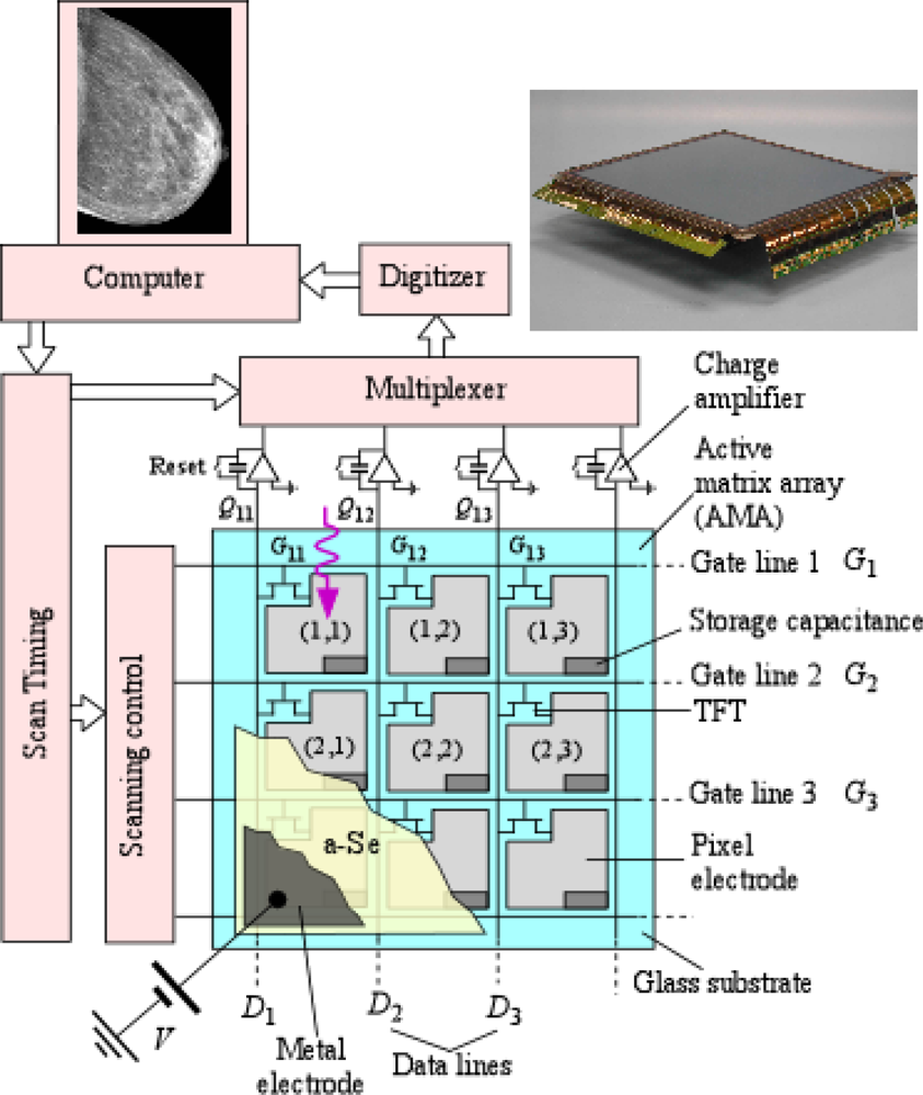


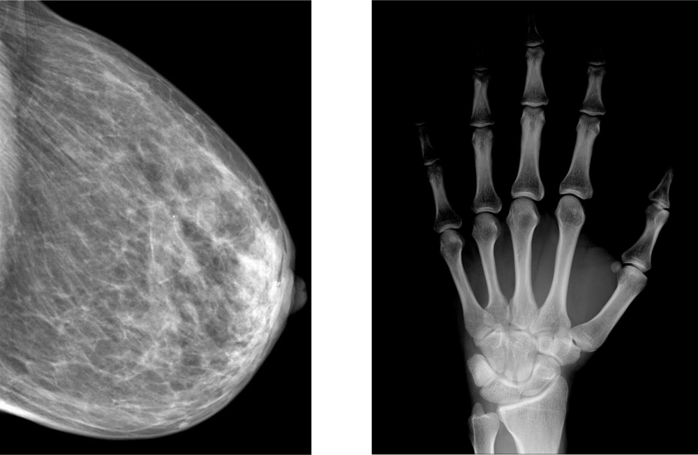

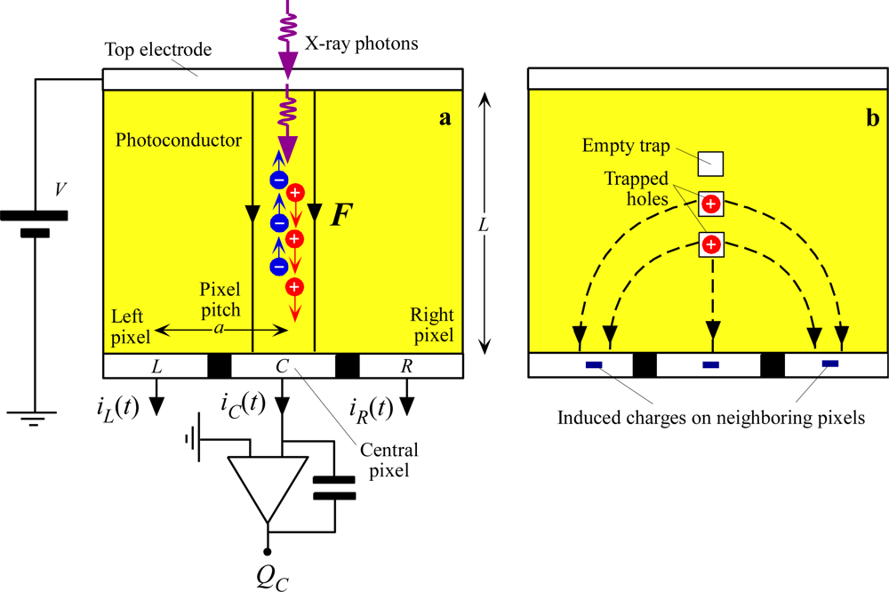


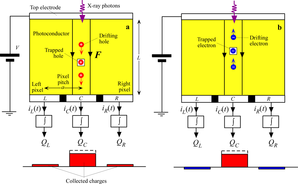


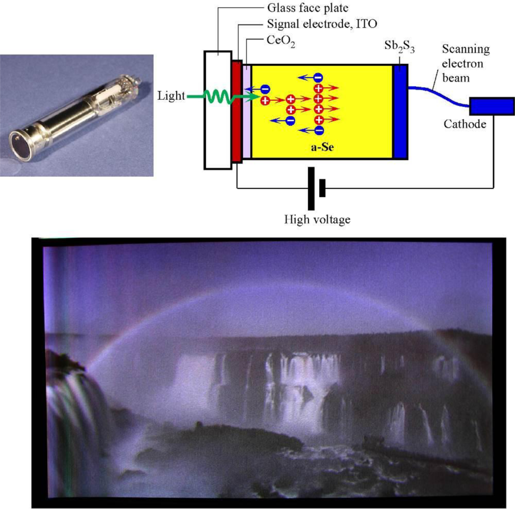
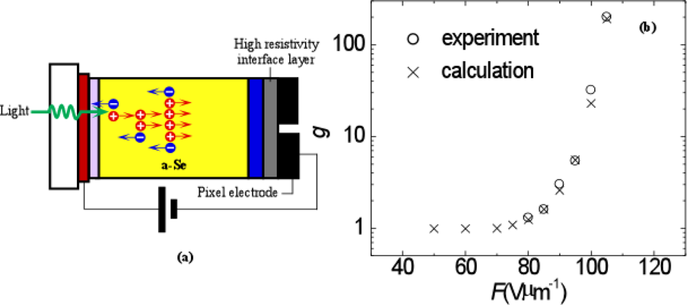
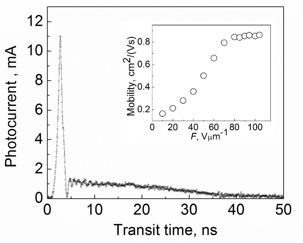


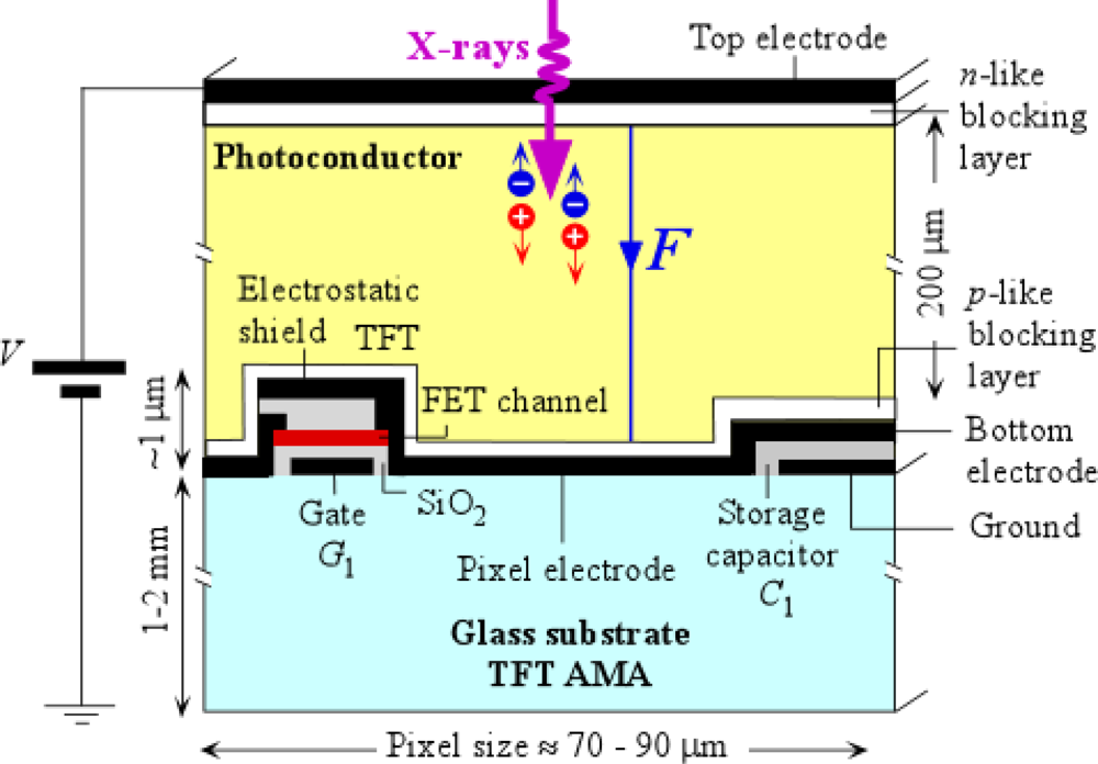
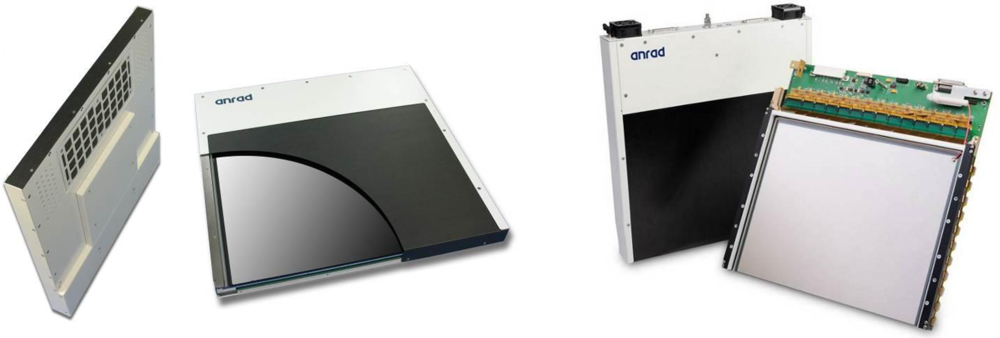
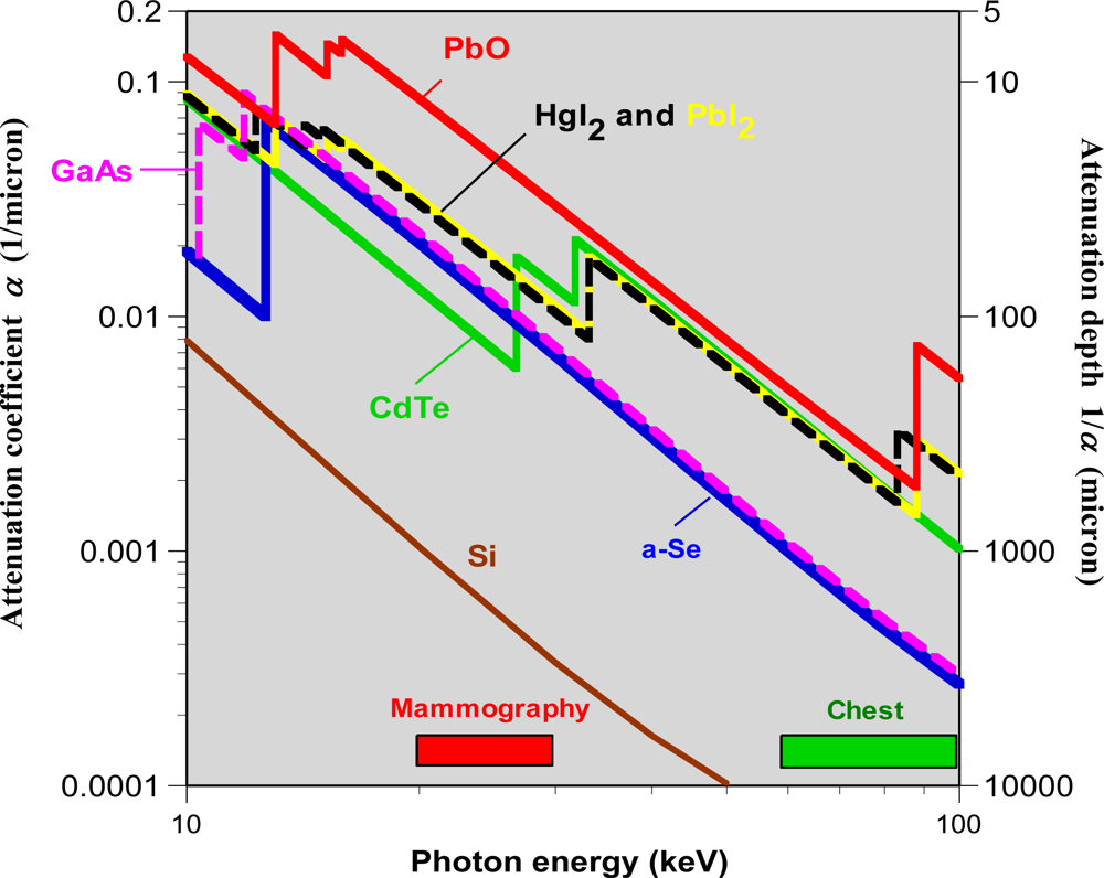
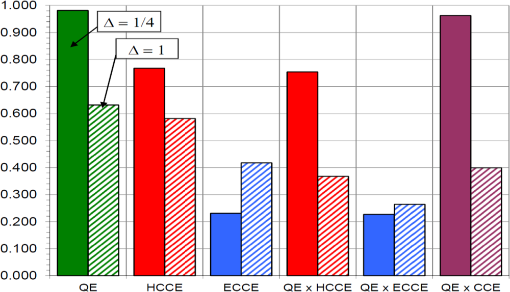
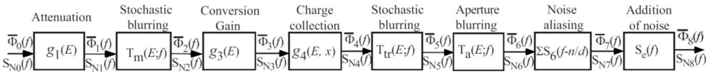
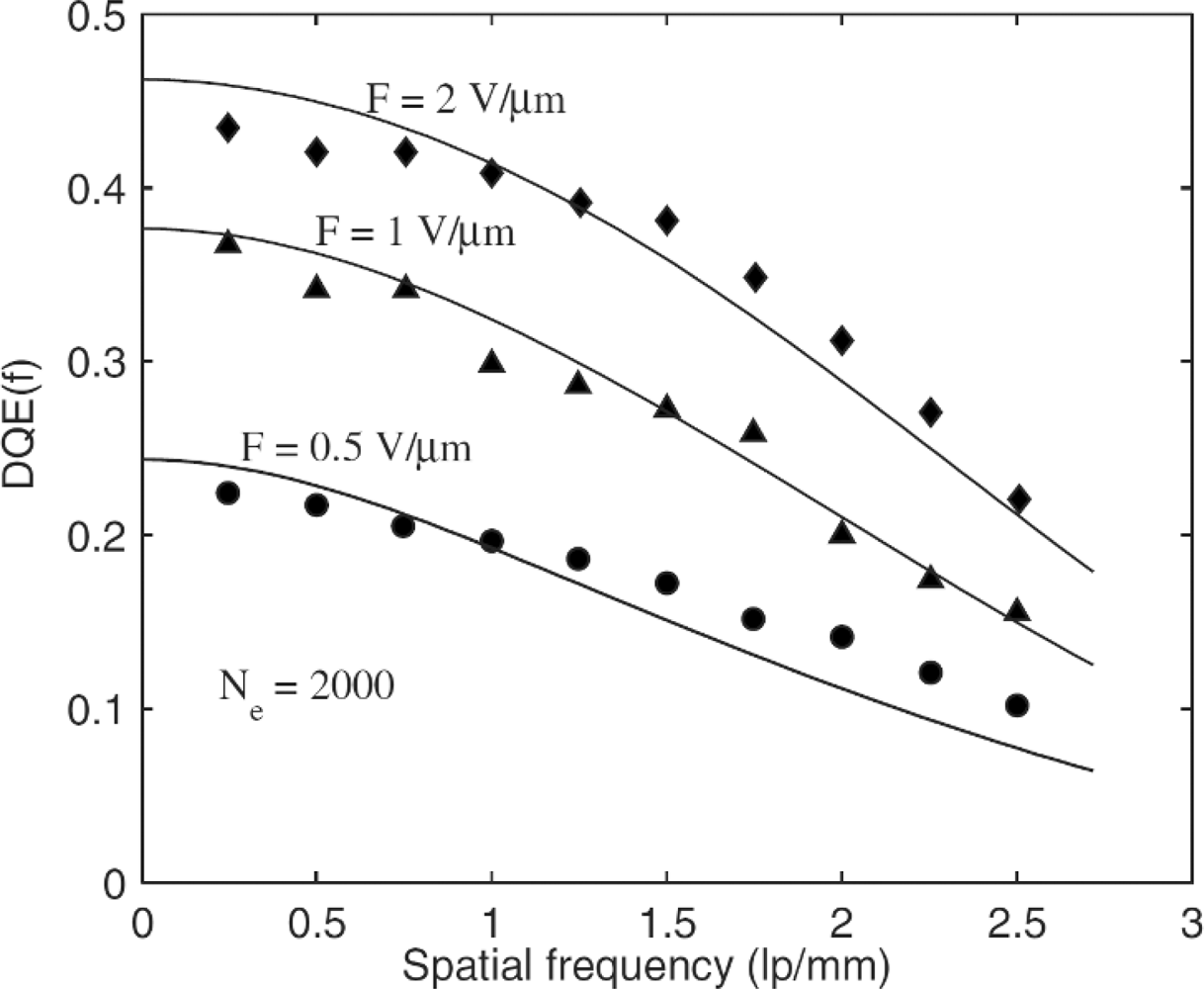
| Photoconductor State Preparation | δ at 20 keV δ at 60 keV | Eg eV | W± eV | Electron μeτe (cm2/V) | Hole μhτh (cm2/V) |
| Stabilized a-Se Amorphous Vacuum deposition [15] | 49 μm 998 μm | 2.2 | 45 at 10 V/μm 20 at 30 V/μm | 3×10⁻⁷–10−5 | 10−6–6 × 10⁻⁵ |
| HgI2 Polycrystalline PVD [68] | 32 μm 252 μm | 2.1 | 5 | 10−5–10−3 | 10−6–10−5 |
| HgI2 Polycrystalline SP [56,68–70] | 32 μm 252 μm | 2.1 | 5 | 10−6–10−5 | ∼10−7 |
| Cd.95Zn.05Te Polycrystalline Vacuum deposition (sublimination) | 80 μm 250 μm | 1.7 | 5 | ∼2 × 10⁻⁴ | ∼3 × 10⁻⁶ |
| PbI2, Polycrystalline Normally PVD [48,49] | 28 μm 259 μm | 2.3 | 5 | 7 × 10⁻⁸ | ∼2 × 10⁻⁶ [71] |
| PbO, Polycrystalline Vacuum deposition | 12 μm 218 μm | 1.9 | 8–20 | 5 × 10⁻⁷ | small |
| TlBr Polycrystalline Vacuum deposition [46] | 18 μm 317 μm | 2.7 | 6.5 | small | 1.5–3 × 10⁻⁶ |
| Phenomenon | Primary observable effects | Comment | Example reference |
|---|---|---|---|
| Hole or electron trapping. The capture of carriers into deep traps. | Reduction in sensitivity Reduction in DQE(0) Reduction in MTF for hole trapping Increase in MTF at high spatial frequencies for electron trapping | Radiation receiving electrode is positive | [82,86–88, 90,91] |
| Hole recombination with previously trapped electrons | Reduction in sensitivity Ghosting | Similar effects if electrons recombine with previously trapped holes | [81] |
| Bulk electron and hole recombination | Reduction in sensitivity Loss of linearity in collected charge vs. exposure | At very high doses that lead to large concentrations of drifting electrons and holes in the bulk. | [95] |
© 2011 by the authors; licensee MDPI, Basel, Switzerland. This article is an open access article distributed under the terms and conditions of the Creative Commons Attribution license (http://creativecommons.org/licenses/by/3.0/).
Share and Cite
Kasap, S.; Frey, J.B.; Belev, G.; Tousignant, O.; Mani, H.; Greenspan, J.; Laperriere, L.; Bubon, O.; Reznik, A.; DeCrescenzo, G.; et al. Amorphous and Polycrystalline Photoconductors for Direct Conversion Flat Panel X-Ray Image Sensors. Sensors 2011, 11, 5112-5157. https://doi.org/10.3390/s110505112
Kasap S, Frey JB, Belev G, Tousignant O, Mani H, Greenspan J, Laperriere L, Bubon O, Reznik A, DeCrescenzo G, et al. Amorphous and Polycrystalline Photoconductors for Direct Conversion Flat Panel X-Ray Image Sensors. Sensors. 2011; 11(5):5112-5157. https://doi.org/10.3390/s110505112
Chicago/Turabian StyleKasap, Safa, Joel B. Frey, George Belev, Olivier Tousignant, Habib Mani, Jonathan Greenspan, Luc Laperriere, Oleksandr Bubon, Alla Reznik, Giovanni DeCrescenzo, and et al. 2011. "Amorphous and Polycrystalline Photoconductors for Direct Conversion Flat Panel X-Ray Image Sensors" Sensors 11, no. 5: 5112-5157. https://doi.org/10.3390/s110505112