Low-Dimensional Palladium Nanostructures for Fast and Reliable Hydrogen Gas Detection

Abstract
: Palladium (Pd) has received attention as an ideal hydrogen sensor material due to its properties such as high sensitivity and selectivity to hydrogen gas, fast response, and operability at room temperature. Interestingly, various Pd nanostructures that have been realized by recent developments in nanotechnologies are known to show better performance than bulk Pd. This review highlights the characteristic properties, issues, and their possible solutions of hydrogen sensors based on the low-dimensional Pd nanostructures with more emphasis on Pd thin films and Pd nanowires. The finite size effects, relative strengths and weaknesses of the respective Pd nanostructures are discussed in terms of performance, manufacturability, and practical applicability.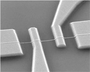
1. Introduction
Hydrogen gas (H2) has attracted a gradually increasing attention as a new energy source, keeping pace with the needs to cope with the anticipated exhaustion of traditional fossil fuels and to alleviate a global warming issue by reducing the use of fossil fuel [1]. Advantages of hydrogen gas lie in its cleanliness, chemical reactivity, recyclability, and natural abundance. However, hydrogen is highly flammable and becomes explosive when its concentration exceeds 4% in air [2]. For this reason, fast and reliable detection of hydrogen gas is required for the wide-spread realization of H2-based applications.
Various approaches have been made to fabricate hydrogen sensors with high sensitivity and fast response [3–11], and some of the initial efforts are typified by the already commercialized hot wire type [12] and electrochemical type [13] sensors. However, those sensors in their early stage of development suffered from drawbacks such as high power consumption, poor hydrogen selectivity, and high operating temperatures. A metal-oxide-semiconductor (MOS) sensor as another type of hydrogen sensor was proposed by Lundström et al., which could detect low concentrations of hydrogen gas [14–19]. This sensor, however, showed weak points such as premature saturation of detectable hydrogen concentrations and low sensitivity. More recently, delicate devices such as metal-oxide-semiconductor field-effect transistors (MOSFETs), and particularly high electron mobility transistors (HEMTs) and metal-semiconductor Schottky diodes, have emerged for high performance H2 sensing [20–25]. Although these devices have achieved much improved sensitivity and reasonable response times and detection limits, the fabrication processes are complicated, making the devices costly. This is because semiconductors incorporated in the structures are generally III–V compounds such as GaN, InGaP, and AlGaAs or II–VI compounds such as ZnO, which are all hard to grow epitaxially with limited growth areas, and many fabrication steps must be carefully controlled to obtain basic device performance along with optimal device design. In these devices, the choice of a catalytic metal is of importance and palladium (Pd) has been the most widely used one for that purpose.
Since the interaction of Pd and hydrogen was comprehensively studied four decades ago [26], the use of Pd has been extensively pursued in fields such as hydrogen storage, hydrogenation of matter, and hydrogen gas sensors [27–35]. Focusing on the hydrogen sensor area, attention has been paid to Pd as a promising H2-sensing material, primarily due to its high sensitivity and selectivity towards H2 and potential compatibility with the conventional integrated circuit (IC) fabrication process [36–38]. More concretely, key requirements for a material to be a good hydrogen sensor include high sensitivity, fast response, high H2 selectivity, room-temperature-operability, good reversibility, low detection limit, and low power consumption. Pd is recognized as a good hydrogen sensor material because it can satisfy most of these key requirements, although its selectivity to hydrogen may change depending on the type of coexisting gases such as CO, CO2, and H2S [39,40]. Needless to say, it is desirable for a Pd-based sensor to meet those requirements simultaneously, which is very challenging. In particular, the parameters of sensitivity, response time, and detection limit are of critical importance in determining the performance of a sensor, and they need to be considered in association with the sensor structures and H2-sensing methods employed.
Representative H2-sensing techniques based on Pd can be categorized as electrical, optical, strain, and chemi-mechanical methods, depending on the physical parameters under detection. Electrical and strain methods measure changes in electrical properties (resistance or conductance) and in sample dimensions, respectively. Sensor geometries for these methods are relatively simple. On the other hand, optical method detects a change in optical properties (reflectance or transmittance) caused by absorption of hydrogen atoms, using optical fibers in most cases. This method is safe, since there is no need to use electric signals that may cause electric discharge and remote sensing in hazardous environments is thus possible. However, light sources such as lasers and rather complex detection systems are required for this method, which makes it weak in both portability and cost-effectiveness [41–44]. Finally, chemi-mechanical methods detect some mechanical change of a small sensing structure. Typical are microcantilevers fabricated by micro-electro-mechanical system (MEMS) processes. The surface of the microcantilevers is usually functionalized with Pd thin films. Volume expansion of a Pd film produced by hydrogen absorption bends the microcantilever and this mechanical change is monitored by parameters such as deflection, resonance frequency, and capacitance. Although this method has the advantages of high sensitivity and low power consumption, several issues such as relatively complex sensor fabrication process, additional signal-detecting systems, and generally slow response still need to be tackled [45–48]. As briefly discussed above, all Pd-based H2-sensing methods have advantages and disadvantages at the same time. Nonetheless, the electrical method is singled out as a central subject in this article because it may have more advantages than others in many aspects such as overall performance level, simplicity of the sensor structures, possibility of sensor miniaturization, manufacturability of the sensors, and compatibility of sensor fabrication process with the current IC process. Conventional electrically operating hydrogen sensors based on Pd are classified as ‘normally-on’ sensors, since they keep conductive before their resistance increase upon H2 exposure. Bulk Pd sensors typically belong to this class.
The recent development of nanotechnologies has fueled the advent of Pd nanostructures such as two-dimensional (2D) Pd thin films [49–53], one-dimensional (1D) Pd nanowires and nanorods [54–58], and even Pd nanoparticles [59–63]. Using these Pd nanostructures, inverse types of ‘on-off’ sensors can be realized, which operate opposite to the conventional hydrogen sensors. In this class of sensors, electrical resistance drops when a sensor material in the initial open state is exposed to H2 [64–68], because a certain type of nanoscopic gap is closed by volume expansion of the Pd nanostructure as demonstrated in Pd mesowire arrays by the Penner group [64]. Although this type of inverse on-off phenomenon is interesting enough, most low-dimensional Pd nanostructures still exhibit resistance-increasing behavior with the adsorption of H2 as in bulk Pd sensors. However, the H2-sensing performance of the Pd nanostructures is in general better than that of bulk Pd, due to the increased surface-to-volume ratio. This is why low-dimensional Pd nanostructures are so widely investigated notwithstanding the increased difficulty in the fabrication of the requisite nanostructures.
In this review article, we present the H2-sensing performance of various sensors employing low-dimensional Pd nanostructures and discuss the finite size effect on the sensor performance, based on results we have obtained up to now. We also highlight issues and possible solutions related to the use of Pd nanostructures. 2D Pd thin films and 1D Pd nanowires are the main subjects of this article with a brief introduction of the use of Pd nanoparticles. The relative strengths and weaknesses of the respective nanostructures are discussed from such various points as performance, manufacturability, and applicability.
2. Fundamentals of Electrical Hydrogen Detection
When a Pd is exposed to H2, hydrogen molecules are adsorbed onto the Pd surface and dissociated into hydrogen atoms [69]. These hydrogen atoms diffuse until they occupy the interstitial sites of the Pd lattice, causing a certain amount of lattice expansion [70,71]. The diffusion generally takes place through high diffusivity paths such as grain boundaries and dislocations or via a vacancy exchange mechanism [70–73], resulting in the defect density dependence of H2 intake. The absorbed hydrogen atoms interact with Pd atoms to form Pd hydrides and increase the frequency of scattering events of charge carriers, which directly leads to the resistance increase of the Pd. In this context, it is expected that the magnitude of resistance increase is proportional to the atomic fraction of absorbed hydrogen atoms to Pd atoms, as expressed by the Sieverts’ law below:
Pick et al. considered such physical factors to calculate the maximum hydrogen in a niobium (Nb) film with a thin Pd overlayer [76]. They found that the maximum atomic fraction of hydrogen atoms inside the Nb film in equilibrium, xmax, was given as:
Given the previous reports that the resistance increase in a film is proportional to hydrogen concentration absorbed in the film, Equation (3) indicates that Pd thin films also obey the Sieverts law mentioned above. Now that the resistance increase in Pd upon exposure to H2 is attributed to the absorbed hydrogen atoms, the concentration of which is strongly correlated with H2 partial pressure in the environment, it would be interesting to identify the key process to determine the absorption process.
Kay et al. demonstrated that the hydrogen absorption rate of Pd is limited by the diffusion process of hydrogen atoms in the bulk rather than the chemisorption of H2 molecules on the surface of the Pd, from an elaborate experiment using a crystalline Pd (110) sheet and a well-designed absorption cell [69]. According to their analyses, a time to half absorption (t1/2), which is the time for the gaseous H2 pressure to reach half of its final value, is given by:
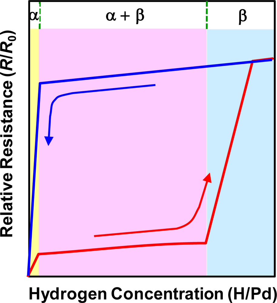
Although the above description illustrates well the general features of the electrical resistance change of Pd in the presence of H2, it is appropriate only for the α phase of the Pd hydride, where a lattice expansion caused by hydrogen filling in the interstitial sites is smaller than 0.13%: a0 = 0.3890 nm for pure Pd vs. aα, max = 0.3895 nm for the upper boundary of the α Pd hydride. As a matter of fact, the Pd hydride, PdHx, exists in a different phase depending on the atomic fraction of hydrogen (x) relative to Pd: α phase when x < 0.015, α + β mixed phase when 0.015 ≤ x < 0.61, and β phase when x > 0.61 at 278 K. Once the concentration of the absorbed hydrogen atoms exceeds the α phase boundary, nuclei of the β phase start to form in the α matrix. The β nuclei grow until the whole original α matrix is transformed to the β phase, where the lattice expansion reaches 3.47%: a0 = 0.3890 nm vs. aβ, min = 0.4025 nm for the lower boundary of the β Pd hydride. The hydrogen concentration range for coexistence of the α and β phases depends on temperature and it grows broader as temperature decreases below ∼300 °C, indicating smaller interstitial sites in the α phase and higher density of imperfections in the β phase at lower temperatures. Sakamoto et al. carefully investigated a relationship between hydrogen gas pressure (pH2), hydrogen concentration in Pd (H/Pd), and relative resistance in the pressure (R/R0) at a specific temperature, using a gas phase method [70]. In contrast with the previous monotonic increase in resistance with hydrogen concentration in Pd, as expressed by Sieverts’ law, they obtained three characteristic regions with different rates of resistance increase. They correspond to the α phase, α + β mixed phase, and β phase, respectively, as schematically shown in Figure 1.
In Figure 1, the resistance traces are different for absorption and desorption processes, which is a characteristic hysteretic resistance behavior of Pd upon cyclic exposure to H2. The abrupt increase in resistance in the β phase region is attributed to the plastic deformation caused mainly by dislocation formation and pile-up. As mentioned above, the appearance of the β phase is dependent on temperature, the steep resistance increase in the β phase and the following hysteresis during desorption process can be alleviated at elevated temperatures. Provided that room-temperature operation is a basic requirement, however, the hysteretic resistance behavior and plastic deformation in the high H/Pd region may be potential serious issues of Pd-based sensors. These issues likely become more serious in low-dimensional Pd structures, in particular, Pd thin films, requiring close investigation on the issues followed by a search for the possible solutions.
3. Two-Dimensional Pd Thin Films
Pd thin films are a basic form of low-dimensional Pd nanostructure, which are easily adaptable to practical hydrogen sensor applications. In these structures, the thickness of the films is usually restricted to less than several hundreds of nm, while the width is flexibly varied to fit into a allowed dimension in the range of several mm to several cm. The very low aspect ratio of film thickness to width generally facilitates hydrogen absorption and desorption processes, and makes the Pd film/substrate interface profoundly important in the cyclic hydrogen sensing. Here, we present the hydrogen-sensing properties of Pd thin films, discuss critical issues related to these film structures, and suggest the possible solutions to tackle the issues.
3.1. Pure Pd Thin Films
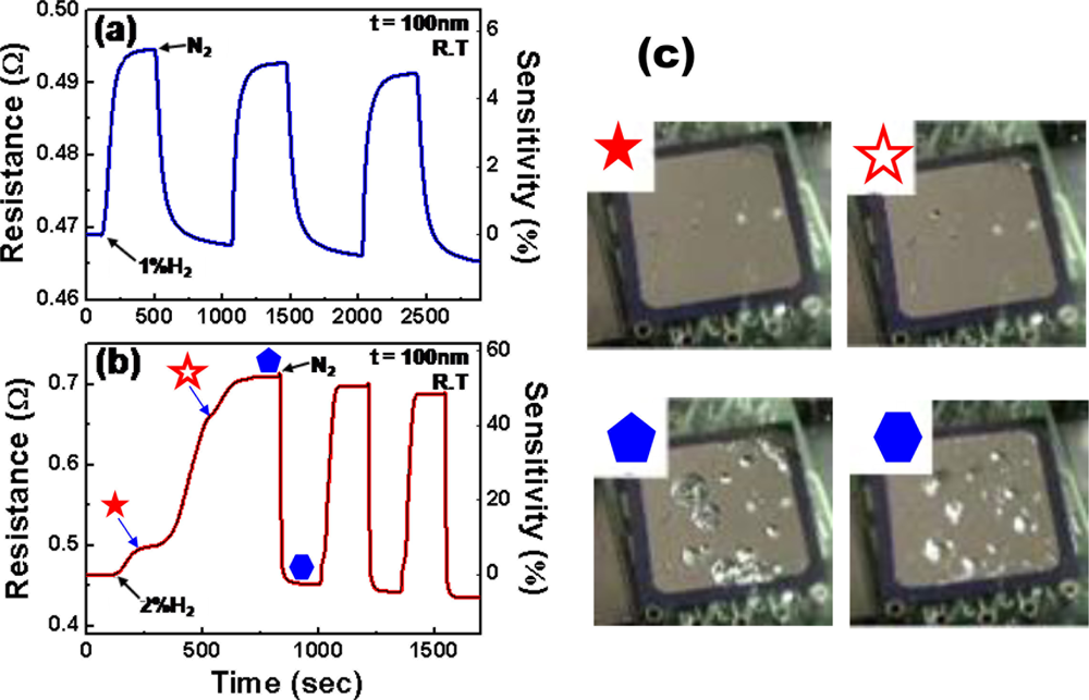
The hydrogen-sensing properties of Pd thin films on thermally oxidized Si substrates were investigated at room temperature, using nitrogen carrier gas (N2). Figure 2 shows the two representative real-time electrical responses of a 100 nm-thick Pd film for 1 and 2% H2. Hereafter, the sensitivity is defined as:
 ) in Figure 2(c)) and the deformations are only partially recovered even after H2 supply is disconnected (see the image (
 ) in Figure 2(c)).
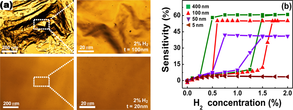
Serious structural deformations can also be observed by confocal laser scanning microscopy. Figure 3(a) shows the microscopic surface scan images of Pd films in exposure to 2% H2, using this technique. The severe film delamination is observed for the Pd film with a thickness of 100 nm, in accordance with the results above. Interestingly, the degree of structural deformations depends on the thickness of Pd film and only small pits are observed on the 20 nm-thick Pd film.
Because the structural deformations are only partially recovered after stopping the H2 flow, they give rise to a hysteresis in resistance vs. H2 concentration curves for a cycle of H2 absorption and desorption processes, as shown in Figure 3(b). The magnitude of the hysteretic behavior, however, decreases with decreasing Pd film thickness, which is well-matched to the tendency observed in thickness-dependent surface deformations. From Figure 3(b), the maximal Pd film thickness, where no hysteresis is observed, is found to be 5 nm, at which the sensitivity is only 4%. It is also difficult to precisely control the thickness as thin as this.
3.2. Pd-Ni Alloy Thin Films
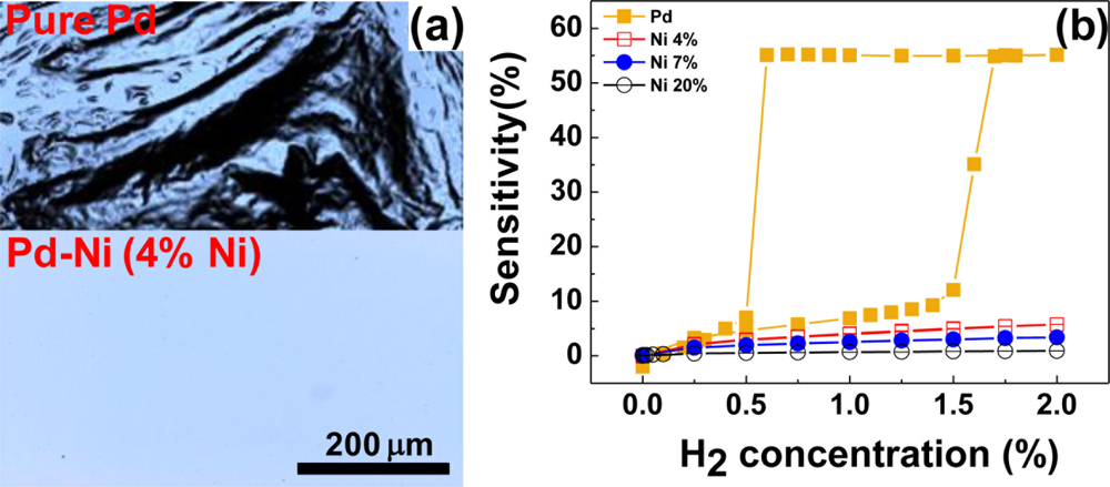
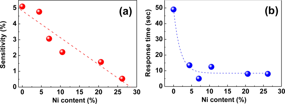
The severe structural deformations and the consequent hysteretic resistance behaviors of pure Pd films should find solutions since they risk the reliability and accuracy of the Pd film-based hydrogen sensors. Various Pd alloys such as Pd-Mg, Pd-Au, Pd-Ag, and Pd-Ni have been explored to enhance the structural stability of the Pd-based thin films of the Pd-based thin films [40,79–82]. Among those, Pd-Au and Pd-Ag alloys have been more studied due to their advantages such as crystal structures similar to that of Pd, higher hydrogen solubilities than pure Pd, and good capabilities to suppress structural deformations. However, they have problematic issues too. For instance, the Au in the Pd-Au alloy easily segregates on the surface owing to its high mobility [83], causing a reliability problem. For the Pd-Ag alloy, good sensor performance, particularly, high hydrogen permeability is observed only in high Ag concentration more than 20 wt% and the hydrogen dissociation capability of the alloy becomes worse than pure Pd in this concentration range [84]. Moreover, both alloys are expensive, adding more cost to sensors incorporating those materials. Comparing Pd-Ni alloy to those alloys, Ni can be introduced to Pd matrix in less amount for suppressing structural deformations. Ni is less likely to segregate in the alloy, is inexpensive, and helps to shorten response times. The attributes of the Pd-Ni alloy like good durability, fast response, and consistency of crystal structure with Pd make it attractive material for hydrogen sensing. According to our investigation, the addition of a small amount of Ni to Pd effectively suppresses the structural deformations, as demonstrated in Figure 4(a). A Pd-Ni alloy containing 4% Ni shows no conceivable surface defects, leading to hysteresis-free resistance change in response to H2 concentration. From Figure 4(b), it is found that the resistances of Pd-Ni alloy films containing more than 4% of Ni increase almost linearly with H2 concentration without a hysteresis, while a pure Pd film shows a sizable hysteretic behavior in its resistance change. Although these results are desirable for sensor operations, the sensitivities of the Pd-Ni alloys are smaller than that of pure Pd. The small sensitivities and linear relationships between the sensitivity and H2 concentration of Pd-Ni alloys are ascribed to a reduced H2 in-take and the hindered β phase formation due to the smaller lattice constants and interstitial volumes and stronger Pd-Ni bonds with respect to pure Pd (see Figure 5(a) below for the dependence of sensitivity on Ni content).
In contrast with the reduced sensitivities, the Pd-Ni alloy films respond to H2 much faster than a pure Pd film, as seen from Figure 5(b).
The response time drastically drops by a factor of ∼5 from the value of a pure Pd when 4% of Ni is added to Pd, and then it remains almost unchanged with further Ni addition. Here, the response time is defined as the time required to reach 36.8% (=e−1) of the total resistance change at a given H2 concentration. Owing to the difference in lattice constants of Pd (3.891 Å) and Ni (3.524 Å), imperfections such as grain boundaries and dislocations are likely to be formed to compensate for the lattice strain generated by the addition of a small amount of Ni to the Pd matrix. These imperfections may function as a preferential diffusion path for the absorbed hydrogen atoms, leading to the shorter response time for Pd-Ni alloys. The steady response time appearing beyond ∼7% Ni stems possibly from the deterioration of crystal quality at high Ni contents rather than the further creation of the line or plane defects. This fast response of the Pd-Ni alloys as well as the sensitivity proportional to H2 concentration makes these alloys a class of good materials for fast, reliable, and scalable H2 sensing.
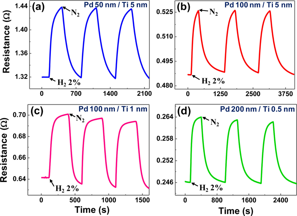
3.3. Pd Thin Films on a Ti Buffer
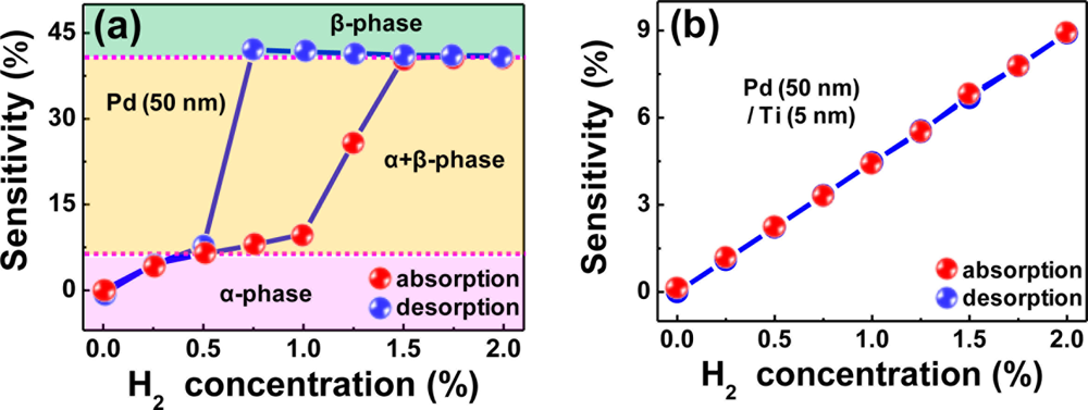
Although the Pd-Ni alloys with a Ni content less than 10% achieved a very fast and hysteresis-free response, the introduction of Ni not only complicates the film preparation, but is also incompatible with the conventional semiconductor integration process. Moreover, the Pd-Ni alloys suffer from a small sensitivity even to high H2 concentration (∼5.5% at 2% H2) and a resistivity increased from the value of Pd even at low Ni content (6 to 7 times at 7% Ni). The structural deformation and hysteretic resistance problems of pure Pd films can be more easily treated using a thin buffer layer. Titanium (Ti) is a typical adhesion promoter for thin films, that is widely used in the present semiconductor industry. We closely examined the effects of a thin Ti buffer layer on the structural and electrical properties of Pd thin films. The film delamination that was a severe problem for pure Pd films was not observed. Real-time electrical responses at room temperature are shown in Figure 6 for Pd/Ti film stacks with different combinations of respective layer thicknesses. All curves exhibit monotonic resistance increase without any intermediate stages, reflecting the absence of structural deformations. Comparing the 100 nm-thick Pd films without (described above) and with Ti buffer layers (5 and 1 nm), the sensitivities (8% and 9.2%) of Ti-buffer Pd films are smaller than that (∼52%) of a pure Pd film.
This indicates that the Ti-mediated improvement in adhesion of Pd film to the substrate strengthens so-called ‘clamping effect’ and restricts global volume expansion of the Pd film [85], lowering the level of H2 in-take and suppressing the appearance of the β hydride. The small increase (only 1.2%) of sensitivity for the thinner Ti buffer reflects that the reinforcement of the clamping effect occurs primarily in the vicinity of Pd film/Ti buffer interface, as also supported by the inflectionless response for even thinner Ti (0.5 nm) in Figure 6(d). Considering the response time, the Ti-buffered Pd films apparently respond to H2 faster (20–30 s for Figure 6(a) through (d)) than does a Pd film with a comparable thickness (∼50 s for 100 nm-thick Pd film). The decreased response time of the Ti-buffered Pd films is attributed to the reduced distance for hydrogen diffusion due to the reduced free volume by the reinforced clamping effect in these film stacks.
As explained above, the structural deformations and hysteretic response behaviors of pure Pd films are associated with phase transitions in them, as represented by Figure 7(a). The β phase grows as H2 concentration increases and the tensile stress produced by volume expansion gradually imposes onto the film/substrate interface. Once this stress exceeds the Pd-substrate bond strength, the Pd film starts to deform until it is delaminated from the substrate, resulting in an abrupt resistance increase. Because these structural deformations are mostly irreversible, there appears a lag in resistance recovery to the α phase value in the desorption process.
The complete phase transition from the α to β phase occurs at ∼1.5% H2. In contrast, the H2 in-take and β phase formation are restricted in the Ti-buffered Pd films due to the enhanced clamping effect, leading to a linear relationship between the sensitivity and H2 concentration in both H2 absorption and desorption processes without a hysteresis, as shown in Figure 7(b). Furthermore, the sensitivity of this Ti-buffered Pd film is larger than that of Pd-Ni alloy films by a factor of 1.6 to 1.7 at a given H2 concentration. The reasonable sensitivity and fast response of the Ti-buffered Pd films without structural deformations and hysteresis, along with a simple fabrication process, allow the film stacks to be considered for practical applications in hydrogen sensors.
3.4. Nanoporous Pd Thin Films
Despite the many strong points the conventional dense Pd films have as hydrogen sensors, they are generally difficult to use for measuring H2 concentration lower than 500 ppm with precision and their response time still needs to be improved. To address these issues, Pd thin films with nanopores have been investigated using anodic aluminum oxide (AAO) templates. The AAO-supported Pd thin films are expected to show a lower H2 detection limit and faster response than the dense Pd films due to the greatly increased surface area. In addition, the film delamination problem may be alleviated in the nanoporous structures owing to the potentially enhanced adhesion provided by the heavy up and down substrate structure. Ding et al. fabricated AAO-supported nanoporous Pd thin films and compared their response characteristics with those of dense Pd films [86]. Notably, the thin porous Pd film could clearly detect H2 concentrations as low as 250 ppm. Comparing the responses of a dense Pd and a porous Pd films with an identical thickness of 45 nm, the resistance change in the porous film was faster and sharper than that of the dense film. The faster and sharper response and lower detection limit of the thin nanoporous Pd film probably originate from the dual contributions of a very thin thickness effect and an enlarged surface effect.
4. One-Dimensional Pd Nanowires
Through the study of nanoporous Pd films described above, it was demonstrated that the H2 detection limit and response time could be reduced in nanoporous structures due to their increased surface area. If it is the real case, Pd nanowires would be ideal structures for fast detection of low H2 concentrations. However, the H2-sensing properties of the Pd nanowires should be considered along with methods for their fabrication, because nanowires are in general harder to fabricate compared to thin films and their properties depend on the final structures. Here, we present the H2-sensing properties of lithographically patterned Pd nanowires, bottom-up grown Pd nanowires, ion-milled Pd nanowires, and grain-structured Pd nanowires. Finite size effects in the Pd nanowires are also discussed.
4.1. Lithographically Patterned Pd Nanowires
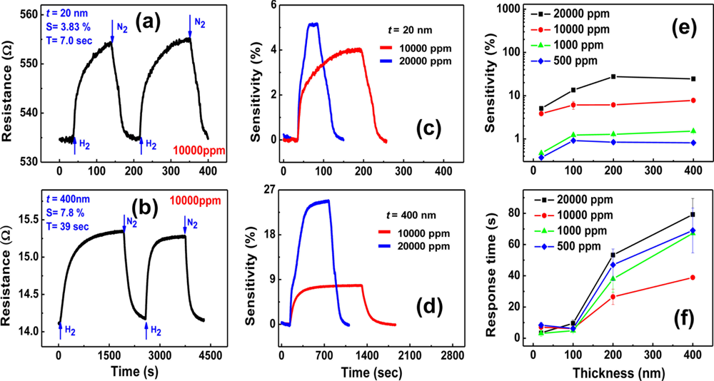
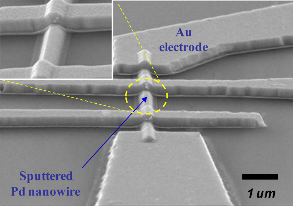
Lithographically patterned Pd nanowires can be regarded as intermediate structures between Pd thin films and bottom-up grown Pd nanowires. To fabricate these nanostructures, a combination of E-beam lithography and a lift-off process was used. Pd thin films with varying thickness t = 20–400 nm were sputter-deposited on thermally oxidized Si substrates. The patterned Pd nanowires had an identical width w = 300 nm and length l = 10 μm. Later, different combinations of a lift-off process and either photolithography or E-beam lithography were used to pattern relatively larger Ti/Au outer electrodes and micron-scaled Ti/Au inner electrodes, respectively, on the Pd nanowires. Figure 8 shows a SEM image of a lithographically patterned Pd nanowire (t = 100 nm) with four inner electrodes.
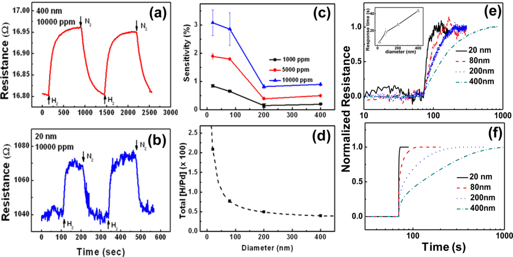
H2-sensing properties of the lithographically patterned Pd nanowires were investigated at room temperature as a function of H2 concentration and nanowire thickness. Typical results are shown in Figure 9. Figures 9(a,b) exhibit electrical responses of two Pd nanowires with t = 20 and 400 nm, respectively, at the same H2 concentration of 10,000 ppm. The thinner nanowire (t = 20 nm) shows a lower sensitivity, but a much faster response time compared to the thicker one (t = 400 nm). This difference is attributed to the stronger clamping effect in the thinner nanowire, as explained in the previous section of Pd thin films. Because the clamping effect originates from the nanowire/substrate interface, it is stronger at positions closer to the interface. The stronger clamping effect in the thinner nanowire suppresses the free volume expansion of the nanowire to limit the hydrogen absorption, leading to a lower sensitivity. The shorter response time is obtained by the reduction of hydrogen diffusion distance in the thinner nanowire.
The relative intensity of the clamping effect can be deduced from the difference in sensitivities to 10,000 and 20,000 ppm H2, as shown in Figures 9(c,d). The ratio of sensitivities to respective 10,000 and 20,000 ppm H2 for the thinner nanowire (t = 20 nm) is only 1.3, in contrast with 3 for the thicker nanowire (t = 400 nm). This indicates that the thinner nanowire absorbs less hydrogen atoms than the thicker one does at the same concentration gradient since the resistance increase upon H2 exposure is basically caused by the enhanced carrier scattering by the absorbed hydrogen atoms, justifying the stronger clamping effect in the thinner Pd nanowire.
Figures 9(e,f) show comprehensive trends of sensitivity and response time as functions of nanowire thickness and H2 concentration. The sensitivity is found to increase with increasing H2 concentration for all thicknesses, as shown in Figure 9(e). However, it is almost saturated beyond a certain thickness, particularly 100 nm at H2 concentrations lower than 10,000 ppm. This may be because the weakening of the clamping effect is counterbalanced by the reduced surface-to-volume ratio in this thickness range. The larger saturation thickness (200 nm) at a higher H2 concentration (20,000 ppm) reflects that the relaxation of the clamping effect is more effective than the reduction of the surface-to-volume ratio at a high H2 partial pressure, probably supported by the slight structural deformation. These sensitivity trends in lithographically patterned Pd nanowires are different from the observations in Pd thin films, where the sensitivity increases with increasing the film thickness in the range of 5 to 400 nm and hysteretic resistance behaviors are observed in all films thicker than 20 nm due to the α to β phase transitions. As a matter of fact, the lithographically patterned Pd nanowires with thicknesses smaller than 100 nm showed an almost linear relationship between the sensitivity and H2 concentration. As a consequence, it was demonstrated that a thin Pd nanowire could detect H2 concentrations as low as 20 ppm.
On the contrary, the response time remains almost constant below 100 nm whereas it gradually decreases with decreasing thickness down to this value. The general decrease of response time with decreasing the thickness is due to the reduced hydrogen diffusion distance mentioned above. The steady response time along with the sensitivity trend in the thickness range smaller than 100 nm suggests that the clamping effect dominates the hydrogen absorption dynamics in this range. The shortest response time obtained from the lithographically patterned Pd nanowires was ∼3 s at 1,000 ppm of H2 for one with t = 20 nm, when the response time is defined as the time required to reach 36.8% (=e−1) of the total resistance change as before. This is much smaller than that of Pd thin films.
4.2. Bottom-Up Grown Pd Nanowires
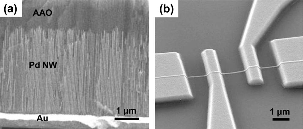
It was found that Pd nanowires fabricated by lithography techniques could be good hydrogen sensors with fast response and low detection limit. However, they possibly face the risk of structural deformations at high H2 concentrations because the nanowire body sticks to the substrate. This problem would be eliminated using bottom-up grown Pd nanowires, which have no direct bonds with the substrate. It would be possible to investigate more intrinsic finite size effects of H2-sensing properties using these Pd nanowires because the clamping effect could be ruled out in these isolated nanowire structures. As an example of this bottom-up approach, Pd nanowires were grown by electrodeposition into nanochannels of AAO templates from an aqueous solution containing 0.034 mol of PdCl2, using an Au cathode layer (see Figure 10(a)).
Pd nanowires were rinsed and immersed in isopropyl alcohol (IPA) after chemically removing the AAO templates. The Pd nanowires were dispersed onto a thermally oxidized Si substrate with patterned outer electrodes on it by a drop-casting method. A combination of E-beam lithography and a lift-off process was used to pattern inner Au electrodes on an individual Pd nanowire. A representative four terminal device on the individual Pd nanowire is shown in Figure 10(b).
H2-sensing properties of the bottom-up grown Pd nanowires were investigated at room temperature as functions of H2 concentration and nanowire diameter in a similar manner for the previous lithographically patterned Pd nanowires. Figures 11(a,b) show representative electrical responses of two Pd nanowires with d = 20 and 400 nm, respectively, at the same H2 concentration of 10,000 ppm. On the contrary to lithographically patterned nanowires with the same thicknesses, the thinner nanowire (d = 20 nm) exhibits a larger sensitivity than that of the thicker one (d = 400 nm). This trend can be confirmed more clearly from the nanowire diameter dependence of the sensitivity shown in Figure 11(c). It is found from this figure that the sensitivity of the Pd nanowire increases with decreasing the nanowire diameter in a range of 0–200 nm for H2 concentrations tested. Since the sensitivity is proportional to the relative concentration of hydrogen atoms in Pd matrix (∝ [H]/[Pd]), this atomic ratio was calculated by the following equation:
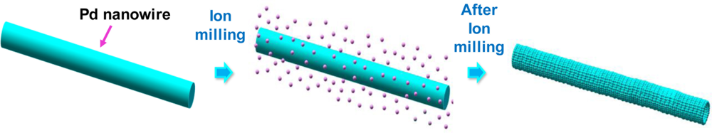
4.3. Ion-Milled Pd Nanowires
From the study of the bottom-up grown Pd nanowires, it was found that the sensitivity increases while the response time decreases as the nanowire diameter shrinks. This was mainly ascribed to the higher density of hydrogen-accommodating sites at the surface compared to the bulk. If this is the case, it would be interesting if we investigate the effects of Pd nanowire surface roughness on the H2-sensing performance because the rough nanowire would provide the larger surface area than the smooth one at the same average diameter. To check this effect, Lee et al. [89] intentionally induced a rough surface on electrodeposition-grown Pd nanowires using ion-milling (beam energy: 500 eV, beam current density: 5 μA/cm2, milling time: 10 min), as shown schematically in Figure 12. The surface of the Pd nanowires, which was initially smooth, appeared to be rough after ion-milling, presumably due to different etch rates depending on crystal planes. They measured electrical responses on individual Pd nanowires before and after ion-milling. Similar device structures to that shown in Figure 10(b) were used for the response measurements. Surprisingly, the resistance of the ion-milled nanowire increased much faster than the as-grown nanowire. When defining the response time as the time required to reach 90% of the total resistance change, the response time of the ion-milled Pd nanowire was found to be approximately 20 times shorter than that of the as-grown one (25 and 500 s, respectively). This is attributed to the enhanced surface-to-volume ratio and the consequent increase of hydrogen-accommodating sites of the ion-milled Pd nanowire. Interestingly, sensitivity seems almost unchanged even through the ion-milling. It may be because the sensitivity depends on the total nanowire volume (average diameter) rather than the surface area.
4.4. Grain-Structured Pd Nanowires
The Pd nanowires grown by electrodeposition into AAO templates described above were structurally homogeneous, resulting in the resistance increase upon H2 exposure. However, many electrodeposited Pd nanowires can have different morphologies depending on the growth conditions. Hu et al. [90] and Yang et al. [91] have demonstrated that the electrodeposited Pd nanowires with different morphologies led to sharp contrasts in their respective response behaviors. Hu et al. grew Pd nanowires on polymethylmethacrylate (PMMA) channels between two Au electrodes by electrophoresis, by varying growth currents [90]. They obtained three different kinds of nanowire structures depending on the nanowire diameter: plain structure at d = 85 nm, grain structure in the range of d = 100–150 nm, and hairy structure at d = ∼100 nm. Interestingly, Pd nanowires with grain structure exhibited the inverse-type of resistance behavior (ΔR/R0 < 0), while normal resistance behaviors (ΔR/R0 > 0) were observed in nanowires with plain structure. The grain-structured nanowires are composed of Pd nanoparticles either in close contact or connected by narrow necks. When these Pd nanowires are exposed to H2, the Pd nanoparticles expand to reduce the length of the neck and the neck itself expands at the same time. These expansions result in an increase in contact area between neighboring nanoparticles, leading to the significant decrease in nanowire resistance. The expanded Pd nanoparticles and necks are back to the original states as soon as H2 flow stops. The grain-structured Pd nanowires could detect H2 concentrations as low as 2–5 ppm. Pd nanowires with hairy structure were subdivided into two different internal structures, which showed normal and inverse resistance behaviors, respectively. The Pd nanowire arrays with grain structures prepared by dielectrophoresis on patterned Si substrates, which was performed by La Ferrara et al. [7], showed a high sensitivity up to 140% at 4% H2. Furthermore, thinner nanowires were found to produce a higher sensitivity and a shorter response time, which is in good agreement with the trend observed in more uniform, isolated Pd nanowires stated above.
5. Pd Nanoparticles
Despite the interesting H2-sensing properties (fast response, reasonable sensitivity, and good reproducibility) of the bottom-up grown homogeneous Pd nanowires, precision diameter control and device fabrication on the nanowires are challenging. Recollecting that the high performance of the nanowires is ascribed to the high surface-to-volume ratio of the structures and high hydrogen-accommodating site density at the surface, Pd nanopartices are expected to show better performance although they have a difficulty in fabrication. Because using a single Pd nanopartice as a sensor medium is extremely difficult, continuous films of Pd nanoparticles or other structures incorporating them have been exploited. Here, we briefly present the examples of using Pd nanoparticles as H2 sensors: continuous films consisting of Pd nanoparticles and Pd nanoparticles grafted onto carbon nanotubes (CNTs).
5.1. Continuous Films of Pd Nanoparticles
Joshi et al. electrochemically deposited Pd nanoparticles on Si substrates by electrodeposition from a solution of Pd sulfate and sulfuric acid [92]. The deposited nanoparticles were dense enough to form a continuous film, as shown schematically in Figure 13.
For sensing performance comparison, sputtered Pd thin films were also prepared in parallel. The average grain sizes of Pd nanoparticle films and sputtered films were varied by either changing deposition time or deposition pressure. The Pd nanoparticle film showed the normal resistance behavior with a resistance increase upon exposure to H2, confirming that the Pd nanoparticles were electrically connected. Referring to Equation (5) for the estimation of sensitivity, the sensitivity was approximately 100% at 1% H2, which was about 70% higher than that of the Pd thin film with the same 150 nm thickness at the same H2 concentration (see Figure 3(b)). This indicates that the continuous film of Pd nanoparticles can detect H2 with larger signals as compared to the normal Pd thin film. The systematic grain-size-dependent comparison study of the sensitivity and response time between the film of Pd nanoparticles and sputtered Pd thin film was carried out. The sensitivity of a Pd nanoparticle film was higher than that of a sputtered Pd thin film at all H2 concentrations and grain sizes, while the response time was shorter in the nanoparticle film than in the sputtered film. Furthermore, for both the nanoparticle film and sputtered film, the sensitivity increased and response time decreased as the average grain size decreases at given H2 concentrations. These results reflect that the enlarged surface-to-volume ratio of the Pd nanoparticles and the higher grain boundary density at a film with smaller grains cooperatively contribute to a higher amount of H2 in-take and a faster hydrogen diffusion. The hydrogen diffusion is also facilitated by the higher density of hydrogen-accommodating sites at the surface of smaller nanoparticles and grains.
5.2. Pd Nanoparticles Grafted onto CNTs
Although the continuous film of Pd nanoparticles demonstrated the improved H2-sensing performance of the nanoparticle systems, it was an intermediate structure between the dense Pd film and a cluster of authentic Pd nanoparticles, consisting of rather large nanoparticles (>14 nm). Moreover, the H2-sensing mechanism was almost the same as for the normal resistance-based H2 sensors. Ju et al. fabricated a different type of H2 sensor, consisting of single-walled CNTs (SWCNTs) as building blocks, truly small Pd nanoparticles (2–3 nm) as H2 absorbers, and dendrimers as grafting mediators of the Pd nanoparticles to SWCNTs [93]. Despite the many advantages of CNTs such as hollow cores, small size, and large surface area, they hardly interact with H2 and need to be functionalized to be used as H2 sensors. Ju et al. first pretreated the SWCNTs to form terminal amine groups on their surfaces and then chemically grew polyamidoamine dendrimers on the surfaces of the pretreated SWCNTs. Subsequently, Pd nanoparticles were grafted onto the dendrimer-modified SWCNTs in aqueous solution of PdCl42− and NaBH4 (see sample 1 in Figure 14). This sample further underwent a pyrolysis (200 °C, 12 h) to remove the dendrimers (see sample 2 in Figure 14).
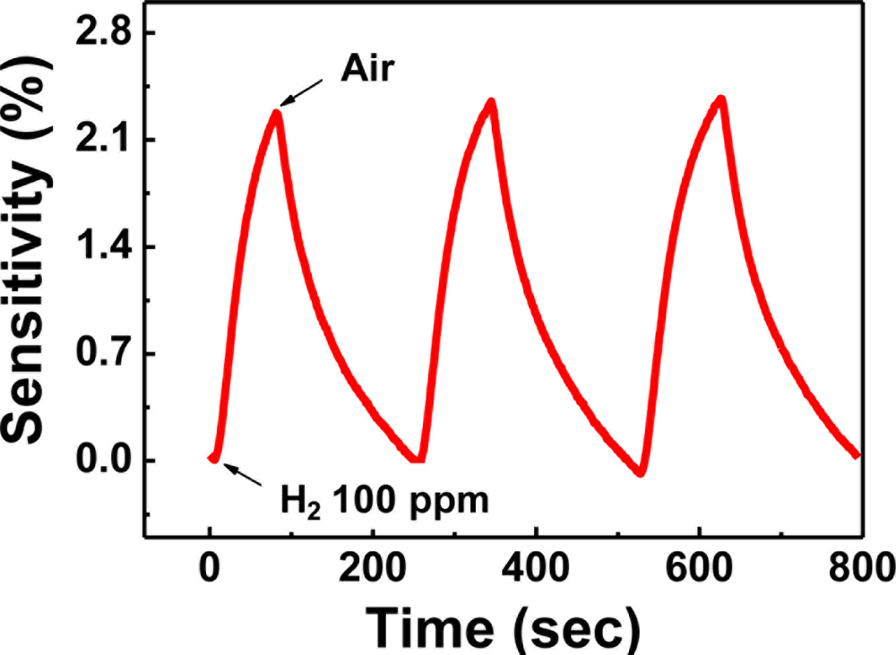
A control sample, where Pd nanoparticles were directly grafted on SWCNTs without dendrimers, were also prepared and Pd nanoparticles appeared to be scarcely formed on its surface. On the other hand, both samples 1 and 2 showed high densities of Pd nanoparticles, confirming the efficacy of the SWCNT modification and nanoparticle-grafting processes. It was believed that the larger nanoparticle size for sample 2 is due to the agglomeration of adjacent nanoparticles during annealing at the elevated temperature (200 °C). Both samples showed normal response behaviors, in which resistance increased upon exposure to H2. Comparing the two samples, sample 2 exhibited a higher sensitivity (25%) and a slightly longer response time (7 s) than those of sample 1 to the same H2 concentration (10,000 ppm). Because both samples behaved like a normal resistance-based H2 sensor, the possibility of engagement of break junctions between Pd nanoparticles should be ruled out. Instead, interactions between the Pd nanoparticles and SWCNTs are the most likely mechanisms to generate such output signals. In this respect, the two samples see different environments and respond differently to H2, mainly depending on the presence or absence of dendrimer layer. It is difficult to transfer absorbed electrons from Pd nanoparticles to SWCNTs due to the dielectric layer in-between them (sample 1). Thus, the dipole moment formation mediated by dendrimers is more likely to be a main player in sample 1. Once dipole moments are formed across the dendrimer layer in response to H2 absorption, the mobility of majority carriers in SWCNTs becomes lower, leading to an increase in resistance. The response time is short because the dipole moments are formed quickly and the sensitivity is rather small because the influence of this phenomenon is not strong. By contrast, the direct electron transfer is possible in sample 2 since Pd nanoparticles are in contact with SWCNTs. Hence, the absorbed hydrogen atoms lower the work function of the Pd nanoparticles and ease the electron transfer from the nanoparticles to SWCNTs. This consequently decreases the hole-carrier density of the p-type SWCNTs, resulting in the resistance increase. Owing to the direct nature and atom level resolution of this mechanism, the sensitivity is high and detection limit is extremely low.
As shown in Figure 15, the response curve of sample 2 is clear and the sensitivity reaches 2.3% at H2 concentration as low as 100 ppm, which is much higher than that of Pd nanowires. The detection limit of 10 ppm H2 in air was achieved using the sample 2.
6. Conclusions
Pd-based hydrogen sensing has been extensively investigated over the past four decades. More recently, the performance of hydrogen sensors has been greatly improved by the use of various Pd nanostructures, which was stimulated by the advancement of nanotechnology. Low-dimensional Pd nanostructures such as Pd thin films, Pd nanowires, and Pd nanoparticles have emerged to meet the requirement of fast, sensitive, and reliable detection of hydrogen gas. Although the nanostructures have many advantages, primarily due to the high surface-to-volume ratio, the manufacturability of hydrogen sensors based on them should be also considered for the practical use of the nanostructured sensors. Hydrogen sensors employing Pd nanostructures have unique attributes and issues that depend on the dimensionality of the nanostructures.
Two-dimensional Pd thin films suffer from structural deformations and hysteretic resistance behaviors although they are the easiest nanostructures to fabricate. These issues hinder the use of Pd films for sensing hydrogen reproducibly and in a scalable way. Use of a proper buffer layer or addition of small amount of second element to Pd can remedy the issues, accompanying the modulated properties such as decreased sensitivity and accelerated response. However, these modified Pd films are confronted with response time and hydrogen detection limit limitations. One-dimensional Pd nanowires show excellent sensor properties in aspects such as hydrogen-sensing scalability, response time, and hydrogen detection limit. However, these nanostructures are difficult to fabricate and their sensitivities fall short of those of Pd thin films. Pd nanoparticles can satisfy almost all the requirements such as high sensitivity, fast response, scalable detection of hydrogen, and low detection limit, if complementary structures are properly chosen.
Acknowledgments
This work was supported by Priority Research Centers Program (2009-0093823) through the National Research Foundation of Korea (NRF).
References and Notes
- Jacobson, M.Z.; Colella, W.G.; Golden, D.M. Cleaning the air and improving health with hydrogen fuel-cell vehicles. Science 2005, 308, 1901–1905. [Google Scholar]
- Liekhus, K.J.; Zlochower, I.A.; Cashdollar, K.L.; Djordjevic, S.M.; Loehr, C.A. Flammability of gas mixtures containing volatile organic compounds and hydrogen. J. Loss Prev. Process Ind 2000, 13, 377–384. [Google Scholar]
- Favier, F. Nanogaps for sensing. Procedia Chem 2009, 1, 746–749. [Google Scholar]
- Cherevko, S.; Kulyk, N.; Fu, J.; Chung, C. Hydrogen sensing performance of electrodeposited conoidal palladium nanowire and nanotube arrays. Sens. Actuat. B 2009, 136, 388–391. [Google Scholar]
- Yang, F.; Taggart, D.; Penner, R. Joule-heating a Palladium nanowire sensor for accelerated response and recovery to hydrogen gas. Small 2010, 6, 1422–1429. [Google Scholar]
- Yang, F.; Kung, S.; Cheng, M.; Hemminger, J.; Penner, R. Smaller is faster and more sensitive: The effect of wire size on the detection of hydrogen by single Palladium nanowires. ACS Nano 2010, 4, 5233–5244. [Google Scholar]
- Ferrara, V.L.; Alfano, B.; Massera, E.; Francia, G.D. Palladium nanowires assembly by dielectrophoresis investigated as hydrogen sensors. IEEE Trans. Nanotech 2008, 7, 776–781. [Google Scholar]
- Ibanez, F.J.; Zamborini, F.P. Ozone- and thermally activated films of Palladium monolayer-protected clusters for chemiresistive hydrogen sensing. Langmuir 2006, 22, 9789–9796. [Google Scholar]
- Sun, Y.; Wang, H.H. Electrodeposition of Pd nanoparticles on single-walled carbon nanotubes for flexible hydrogen sensors. Appl. Phys. Lett 2007, 90, 213107–213113. [Google Scholar]
- Schlecht, U.; Balasubramanian, K.; Burghard, M.; Kern, K. Electrochemically decorated carbon nanotubes for hydrogen sensing. Appl. Surf. Sci 2007, 253, 8394–8397. [Google Scholar]
- Sun, Y.; Wang, H.H.; Xia, M. Single-walled carbon nanotubes modified with Pd nanoparticles: Unique building blocks for high-performance, flexible hydrogen sensors. J. Phys. Chem. C 2008, 112, 1250–1259. [Google Scholar]
- Katsuki, A.; Fukui, K. H2 selective gas sensor based on SnO2. Sens. Actuat. B 1998, 52, 30–37. [Google Scholar]
- Bakker, E.; Telting-Diaz, M. Electrochemical sensors. Anal. Chem 2002, 74, 2781–2800. [Google Scholar]
- Lundström, I.; Shivaraman, S.; Svensson, C.; Lundkvist, L. A hydrogen-sensitive MOS field effect transistor. Appl. Phys. Lett 1975, 26, 55–57. [Google Scholar]
- Johansson, M.; Lundström, I.; Ekedahl, L.G. Bridging the pressure gap for palladium metal-insulator-semiconductor hydrogen sensors in oxygen containing environments. J. Appl. Phys 1998, 84, 44–51. [Google Scholar]
- Liu, W.; Pan, H.; Chen, H.; Lin, K.; Wang, C. Comparative hydrogen-sensing study of Pd/GaAs and Pd/InP metal-oxide-semiconductor Schottky diodes. J. Appl. Phys 2001, 40, 6254–6259. [Google Scholar]
- Lu, C.T.; Lin, K.W.; Chen, H.I.; Chuang, H.M.; Chen, C.Y.; Liu, W.C. A new Pd-oxide-Al0.3Ga0.7As MOS hydrogen sensor. IEEE Electron. Dev. Lett 2003, 24, 390–392. [Google Scholar]
- Kang, B.S.; Ren, F.; Gila, B.P.; Abernathy, C.R.; Pearton, S.J. AlGaN/GaN-based metal-oxide-semiconductor diode-based hydrogen gas sensor. Appl. Phys. Lett 2004, 84, 1123–1125. [Google Scholar]
- Fang, Y.K.; Hwang, S.B.; Lin, C.Y.; Lee, C.C. Trench Pd/Si metal-oxide-semiconductor Schottky barrier diode for a high sensitivity hydrogen gas sensor. Appl. Phys. Lett 2009, 57, 2686–2688. [Google Scholar]
- Cheng, C.C.; Tsai, Y.Y.; Lin, K.W.; Chen, H.I.; Hsu, W.H.; Hung, C.W.; Liu, R.C.; Liu, W.C. Pd-oxide-Al0.24Ga0.76As (MOS) high electron mobility transistor (HEMT)-based hydrogen sensor. IEEE Sens. J 2006, 6, 287–292. [Google Scholar]
- Cheng, C.C.; Tsai, Y.Y.; Lin, K.W.; Chen, H.I.; Hsu, W.H.; Hong, C.W.; Liu, W.C. Characteristics of a Pd-oxide-In0.49Ga0.51P high electron mobility transistor (HEMT)-based hydrogen sensor. Sens. Actuat. B 2006, 113, 29–35. [Google Scholar]
- Hung, C.; Lin, H.; Chen, H.; Tsai, Y.; Lai, P.; Fu, S.; Chuang, H.; Liu, W. Comprehensive study of a Pd-GaAs high electron mobility transistor (HEMT)-based hydrogen sensor. Sens. Actuat. B 2007, 122, 81–88. [Google Scholar]
- Kang, B.S.; Wang, H.T.; Ren, F.; Pearton, S.J.; Morey, T.E.; Dennis, D.M.; Johnson, J.W.; Rajagopal, P.; Roberts, J.C.; Piner, E.L.; Linthicum, K.J. Enzymatic glucose detection using ZnO nanorods on the gate region of AlGaN/GaN high electron mobility transistors. Appl. Phys. Lett 2007, 91, 252103–252105. [Google Scholar]
- Yu, X.; Li, C.; Low, Z.N.; Lin, J.; Anderson, T.J.; Wang, H.T.; Ren, F.; Wang, Y.L.; Chang, C.Y.; Pearton, S.J.; Hsu, C.H.; Osinsky, A.; Dabiran, A.; Chow, P.; Balaban, C.; Painter, J. Wireless hydrogen sensor network using AlGaN/GaN high electron mobility transistor differential diode sensors. Sens. Actuat. B 2008, 135, 188–194. [Google Scholar]
- Anderson, T.; Ren, F.; Pearton, S.; Kang, B.S.; Wang, H.T.; Chang, C.Y.; Lin, J. Advances in hydrogen, carbon dioxide, and hydrocarbon gas sensor technology using GaN and ZnO-based devices. Sensors 2009, 9, 4669–4694. [Google Scholar]
- Lewis, F.A. The Palladium Hydrogen System; Academic Press: London, UK, 1967. [Google Scholar]
- Kolb, G.; Zapf, R.; Hessel, V.; Löwe, H. Propane steam reforming in micro-channels—results from catalyst screening and optimization. Appl. Catal. A 2004, 277, 155–166. [Google Scholar]
- Züttel, A.; Wenger, P.; Sudan, P.; Mauron, P; Orimo, S.I. Hydrogen density in nanostructured carbon, metals and complex materials. Mater. Sci. Eng. B 2004, 108, 9–18. [Google Scholar]
- Kishorea, S.; Nelsonb, J.A.; Adairb, J.H.; Eklund, P.C. Hydrogen storage in spherical and platelet palladium nanoparticles. J. Alloys Compd 2005, 389, 234–242. [Google Scholar]
- Zacharia, R.; Kim, K.Y.; Kibria, A.K.M.F.; Nahm, K.S. Enhancement of hydrogen storage capacity of carbon nanotubes via spill-over from vanadium and palladium nanoparticles. Chem. Phys. Lett 2005, 412, 369–375. [Google Scholar]
- Strukul, G.; Gavagnin, R.; Pinna, F.; Modaferri, E.; Perathoner, S.; Centi, G.; Marella, M.; Tomaselli, M. Use of palladium based catalysts in the hydrogenation of nitrates in drinking water: From powders to membranes. Catal. Today 2000, 55, 139–149. [Google Scholar]
- Dittmeyer, R.; Höllein, V.; Daub, K. Membrane reactors for hydrogenation and dehydrogenation processes based on supported palladium. J. Mol. Catal. A 2001, 173, 135–184. [Google Scholar]
- Yamauchi, M.; Ikeda, R.; Kitagawa, H.; Takata, M. Nanosize effects on hydrogen storage in Palladium. ACS Nano 2008, 112, 3294–3299. [Google Scholar]
- Sekimoto, S.; Nakagawa, H.; Okazaki, S.; Fukuda, K.; Asakura, S.; Shigemori, T.; Takahashi, S. A fiber-optic evanescent-wave hydrogen gas sensor using palladium-supported tungsten oxide. Sens. Actuat. B 2000, 66, 142–145. [Google Scholar]
- Roy, S.; Jacob, C.; Basu, S. Studies on Pd/3C-SiC Schottky junction hydrogen sensors at high temperature. Sens. Actuat. B 2003, 94, 298–303. [Google Scholar]
- Tabib-Azar, M.; Sutapun, B.; Petrick, R.; Kazemi, A. Highly sensitive hydrogen sensors using palladium coated fiber optics with exposed cores and evanescent field interactions. Sens. Actuat. B 1999, 56, 158–163. [Google Scholar]
- Flanagan, T.B.; Oates, W.A. The palladium-hydrogen system. Annu. Rev. Mater. Sci 1991, 21, 269–304. [Google Scholar]
- Frazier, G.A.; Glosser, R. Characterization of thin films of the palladium-hydrogen system. Less-Common Met 1980, 74, 89–96. [Google Scholar]
- Way, J.D.; Thoen, P.M. Palladium/Copper Alloy Composite Membranes for High Temperature Hydrogen Separation; Final Technical Progress Report; Energy Citations Database (ECD):: Washington, DC, USA; 31; August; 2006. [Google Scholar]
- Cheng, Y.T.; Li, Y.; Lisi, D.; Wang, W.M. Preparation and characterization of Pd/Ni thin films for hydrogen sensing. Sens. Actuat. B 1996, 30, 11–16. [Google Scholar]
- Lieberman, R.A.; Beshay, M.H. Safe detector system for hydrogen leaks. Proceedings of 2010 DOE Hydrogen Program Annual Merit Review and Peer Evaluation, Washington, DC, USA, 7–11 June 2010.
- Maier, R.R.J.; Jones, B.J.S.; Barton, J.S.; McCulloch, S.; Allsop, T.; Jones, J.D.C.; Bennion, I. Fibre optics in palladium-based hydrogen sensing. J. Opt. A Pure Appl. Opt 2007, 9, S45–S59. [Google Scholar]
- Okuhara, Y.; Takata, M. Recovery characteristics of optical hydrogen sensor using Pd thin film: Behaviour of three-stage hydrogen desorption. Bull. Mater. Sci 1999, 22, 85–87. [Google Scholar]
- Shim, J.Y.; Lee, J.D.; Jin, J.M.; Cheong, H. Comparison of Pd, Pt and Pt/Pd as catalysts for hydrogen sensor films. J. Korean Phys. Soc 2009, 55, 2693–2696. [Google Scholar]
- Patton, J.F.; Hunter, S.R.; Sepaniak, M.J.; Daskos, P.G.; Smith, D.B. Rapid response microsensor for hydrogen detection using nanostructured palladium films. Sens. Actuat. A 2010, 163, 464–470. [Google Scholar]
- Chou, Y.I.; Chiang, H.C.; Wang, C.C. Study on Pd functionalization of microcantilever for hydrogen detection promotion. Sens. Actuat. B 2008, 129, 72–78. [Google Scholar]
- Baselt, D.R.; Fruhberger, B.; Klaassen, E.; Cemalovic, S.; Britton, C.L.; Patel, S.V.; Mlsna, T.E.; Warmack, D.M.B. Design and performance of a microcantilever-based hydrogen. Sens. Actuat. B 2003, 88, 120–131. [Google Scholar]
- Fabre, A.; Finot, E.; Demoment, J.; Contreras, S. Monitoring the chemical changes in Pd induced by hydrogen absorption using microcantilevers. Ultramicroscopy 2003, 97, 425–432. [Google Scholar]
- Cabrera, A.L.; Aguayo-Soto, R. Hydrogen absorption in palladium films sensed by changes in their resistivity. Catalysis Lett 1997, 45, 79–83. [Google Scholar]
- Xu, T.; Zach, M.P.; Xiao, Z.L.; Rosenmann, D.; Welp, U.; Kwok, W.K.; Crabtree, G.W. Self-assembled monolayer-enhanced hydrogen sensing with ultrathin palladium films. Appl. Phys. Lett 2005, 86, 2031041–2031043. [Google Scholar]
- Hughes, R.C.; Schubert, W.K. Thin films of Pd/Ni alloys for detection of high hydrogen concentrations. J. Appl. Phys 1992, 71, 542–544. [Google Scholar]
- Mandelis, A.; Garcia, J.A. Pd/PVDF thin film hydrogen sensor based on laser-amplitude-modulated optical-transmittance: Dependence on H2 concentration and device physics. Sens. Actuat. B 1998, 49, 258–267. [Google Scholar]
- Zhao, Z.; Carpenter, M.A.; Xia, H.; Welch, D. All-optical hydrogen sensor based on a high alloy content palladium thin film. Sens. Actuat. B 2006, 113, 532–538. [Google Scholar]
- Yun, M.H.; Myung, N.V.; Vasquez, R.P.; Lee, C.; Menke, E.; Penner, R.M. Electrochemically grown wires for individually addressable sensor arrays. Nano Lett 2004, 4, 419–422. [Google Scholar]
- Im, Y.H.; Lee, C.; Vasquez, R.P.; Bangar, M.A.; Myung, N.V.; Menke, E.J.; Penner, R.M.; Yun, M.H. Investigation of a single Pd nanowire for use as a hydrogen sensor. Small 2006, 2, 356–358. [Google Scholar]
- Walter, E.C.; Favier, F.; Penner, R.M. Palladium mesowire arrays for fast hydrogen sensors and hydrogen-actuated switches. Anal. Chem 2002, 74, 1546–1553. [Google Scholar]
- Atashbar, M.Z.; Banerji, D.; Singamaneni, S. Room-temperature hydrogen sensor based on palladium nanowires. IEEE Sens. J 2005, 5, 792–797. [Google Scholar]
- Kim, K.T.; Sim, J.; Cho, S.M. Hydrogen gas sensor using Pd nanowires electro-deposited into anodized alumina template. IEEE Sens. J 2006, 6, 509–513. [Google Scholar]
- Kong, J.; Chapline, M.G.; Dai, H. Functionalized carbon nanotubes for molecular hydrogen sensors. Adv. Mater 2001, 13, 1384–1386. [Google Scholar]
- Mubeen, S.; Zhang, T.; Yoo, B.; Deshusses, M.A.; Myung, M.V. Palladium nanoparticles decorated single-walled carbon nanotube hydrogen sensor. J. Phys. Chem. C 2007, 111, 6321–6327. [Google Scholar]
- Zhao, Q.; Gan, Z.; Zhuang, Q. Electrochemical sensors based on carbon nanotubes. Electroanalysis 2002, 14, 1609–1613. [Google Scholar]
- Sun, Y.; Wang, H.H. High-performance, flexible hydrogen sensors that use carbon nanotubes decorated with Palladium nanoparticles. Adv. Mater 2007, 19, 2818–2823. [Google Scholar]
- Kolmakov, A.; Klenov, D.O.; Lilach, Y.; Stemmer, S.; Moskovits, M. Enhanced gas sensing by individual SnO2 nanowires and nanobelts functionalized with Pd catalyst particles. Nano Lett 2005, 5, 667–673. [Google Scholar]
- Favier, F.; Walter, E.C.; Zach, M.P.; Benter, T.; Penner, R.M. Hydrogen sensors and switches from electrodeposited palladium mesowire arrays. Science 2001, 293, 2227–2231. [Google Scholar]
- Atashbar, M.Z.; Singamaneni, S. Room temperature gas sensor based on metallic nanowires. Sens. Actuat. B 2005, 111, 13–21. [Google Scholar]
- Dasari, R.; Zamborini, F.P. Hydrogen switches and sensors fabricated by combining electropolymerization and Pd electrodeposition at microgap electrodes. J. Am. Chem. Soc 2008, 130, 16138–16139. [Google Scholar]
- Hatakeyama, Y.; Umetsu, M.; Ohara, S.; Kawadai, F.; Takami, S.; Naka, T.; Adschiri, T. Homogenous spherical mosslike assembly of Pd nanoparticles by using DNA compaction: application of Pd-DNA hybrid materials to volume-expansion hydrogen switches. Adv. Mater 2008, 20, 1122–1128. [Google Scholar]
- Ohara, S.; Hatakeyama, Y.; Umetsu, M.; Sato, K.; Naka, T.; Adschiri, T. Palladium-polyelectrolyte hybrid nanoparticles for hydrogen sensor in fuel cells. J. Power Sources 2009, 193, 367–370. [Google Scholar]
- Kay, B.D.; Peden, C.H.F.; Goodman, D.W. Kinetics of hydrogen absorption by Pd(110). Phys. Rev. B 1986, 34, 817–822. [Google Scholar]
- Sakamoto, Y.; Takai, K.; Takashima, I.; Imada, M. Electrical resistance measurements as a function of composition of palladium-hydrogen(deuterium) systems by a gas phase method. J. Phys. Condens. Matter 1996, 8, 3399–3411. [Google Scholar]
- Smith, R.J.; Otterson, D.A. Electrical resistivity of PdHx system for H/Pd atom ratios to 0.97. J. Phys. Chem. Solids 1970, 31, 187–189. [Google Scholar]
- Pundt, A.; Kirchheim, R. Hydrogen in metals: Microstructural aspects. Annu. Rev. Mater. Res 2006, 36, 555–608. [Google Scholar]
- Fukai, Y.; Sugimoto, H. Formation mechanism of defect metal hydrides containing superabundant vacancies. J. Phys. Condens. Matter 2007, 19, 4362011–43620124. [Google Scholar]
- Sieverts, A. Absorption of Gases by Metals. Z. Metallkund 1929, 21, 37. [Google Scholar]
- Mueller, W.M.; Blackledge, J.P.; Libowitz, G.G. Metal Hydrides; Academic Press: New York, NY, USA, 1968. [Google Scholar]
- Pick, M.A.; Davenport, J.W.; Strongin, M.; Dienes, G.J. Enhancement of hydrogen uptake rates for Nb and Ta by thin surface overlayers. Phys. Rev. Lett 1979, 43, 286–289. [Google Scholar]
- Lee, E.; Lee, J.M.; Koo, J.H.; Lee, W.; Lee, T. Hysteresis behavior of electrical resistance in Pd thin films during the process of absorption and desorption of hydrogen gas. Int. J. Hydrogen Energ 2010, 35, 6984–6991. [Google Scholar]
- Kim, K.R.; Noh, J.S.; Lee, J.M.; Kim, Y.J.; Lee, W. Suppression of phase transitions in Pd thin filmsby insertion of a Ti buffer layer. J. Mater. Sci 2010. [Google Scholar] [CrossRef]
- Nakano, S.; Yamaura, S.; Uchinashi, S.; Kimura, H.; Inoue, A. Effect of hydrogen on the electrical resistance of melt-spun Mg90Pd10 amorphous alloy. Sens. Actuat. B 2005, 104, 75–79. [Google Scholar]
- Huang, X.M.H.; Manolidis, M.; Jun, S.C.; Hone, J. Nanomechanical hydrogen sensing. Appl. Phys. Lett 2005, 86, 1431041–1431043. [Google Scholar]
- Wang, M.; Feng, Y. Palladium-silver thin film for hydrogen sensing. Sens. Actuat. B 2007, 123, 101–106. [Google Scholar]
- Lee, E.; Lee, J.M.; Noh, J.S.; Joe, J.H.; Lee, W. Hydrogen gas sensing performance of Pd-Ni alloy thin films. Thin Solid Films 2010, 519, 880–884. [Google Scholar]
- Butler, M.A.; Sanchez, R.; Dulleck, G.R. Fiber Optic Hydrogen Sensor; Sandia Report SAND-96-1 133; Sandia National Labs: Albuquerque, NM, USA, 1996. [Google Scholar]
- Gielens, F.C.; Tong, H.D.; van Rijn, C.J.M.; Vorstman, M.A.G.; Keurentjes, J.T.F. Microsystem technology for high-flux hydrogen separation membranes. J. Membr. Sci 2004, 243, 203–213. [Google Scholar]
- Nicolas, M.; Dumoulin, L.; Burger, J.P. Thickness dependence of the critical solution temperature of hydrogen in Pd films. J. Appl. Phys 1986, 60, 3125–3130. [Google Scholar]
- Ding, D.; Chen, Z.; Lu, C. Hydrogen sensing of nanoporous palladium films supported by anodic aluminum oxides. Sens. Actuat. B 2006, 120, 182–186. [Google Scholar]
- Jeon, K.J.; Lee, J.M.; Lee, E.; Lee, W. Individual Pd nanowire hydrogen sensors fabricated by electron-beam lithography. Nanotechnology 2009, 20, 1355021–1355025. [Google Scholar]
- Jeon, K.J.; Jeun, M.; Lee, E.; Lee, J.M.; Lee, K.I.; von Allmen, P.; Lee, W. Finite size effect on hydrogen gas sensing performance in single Pd nanowires. Nanotechnology 2008, 19, 4955011–4955016. [Google Scholar]
- Lee, J.M.; Lee, W. Effects of surface roughness on hydrogen gas sensing properties of single Pd nanowires. J. Nanosci. Nanotech 2010. submitted.. [Google Scholar]
- Hu, Y.; Perello, D.; Mushtaq, U.; Yun, M. A single palladium nanowire via electrophoresis deposition used as a ultrasensitive hydrogen sensor. IEEE T. Nanotechnol 2008, 7, 693–699. [Google Scholar]
- Yang, F.; Taggart, D.K.; Penner, R.M. Fast, sensitive hydrogen gas detection using single palladium nanowires that resist fracture. Nano Lett 2009, 9, 2177–2182. [Google Scholar]
- Joshi, R.K.; Krishnan, S.; Yoshimura, M.; Kumar, A. Pd nanoparticles and thin films for room temperature hydrogen sensor. Nanoscale Res. Lett 2009, 4, 1191–1196. [Google Scholar]
- Ju, S.; Lee, J.M.; Jung, Y.; Lee, E.; Lee, W.; Kim, S.J. Highly sensitive hydrogen gas sensors using single-walled carbon nanotubesgrafted with Pd nanoparticles. Sens. Actuat. B 2010, 146, 122–128. [Google Scholar]


© 2011 by the authors; licensee MDPI, Basel, Switzerland. This article is an open access article distributed under the terms and conditions of the Creative Commons Attribution license (http://creativecommons.org/licenses/by/3.0/).
Share and Cite
Noh, J.-S.; Lee, J.M.; Lee, W. Low-Dimensional Palladium Nanostructures for Fast and Reliable Hydrogen Gas Detection. Sensors 2011, 11, 825-851. https://doi.org/10.3390/s110100825
Noh J-S, Lee JM, Lee W. Low-Dimensional Palladium Nanostructures for Fast and Reliable Hydrogen Gas Detection. Sensors. 2011; 11(1):825-851. https://doi.org/10.3390/s110100825
Chicago/Turabian StyleNoh, Jin-Seo, Jun Min Lee, and Wooyoung Lee. 2011. "Low-Dimensional Palladium Nanostructures for Fast and Reliable Hydrogen Gas Detection" Sensors 11, no. 1: 825-851. https://doi.org/10.3390/s110100825