Recent Advances in the Design of Electro-Optic Sensors for Minimally Destructive Microwave Field Probing

Abstract
: In this paper we review recent design methodologies for fully dielectric electro-optic sensors that have applications in non-destructive evaluation (NDE) of devices and materials that radiate, guide, or otherwise may be impacted by microwave fields. In many practical NDE situations, fiber-coupled-sensor configurations are preferred due to their advantages over free-space bulk sensors in terms of optical alignment, spatial resolution, and especially, a low degree of field invasiveness. We propose and review five distinct types of fiber-coupled electro-optic sensor probes. The design guidelines for each probe type and their performances in absolute electric-field measurements are compared and summarized.1. Introduction
Over the past two decades, electro-optic (EO) sensing technologies have been continually and viably developed as a practical and unique method for sensing electric fields in a minimally destructive way [1–6]. This is because EO crystals are essentially transparent to both electromagnetic and optical waves. The unique, electrically-transparent aspect of these all-dielectric field probes enables exploration of the near-electric-field distributions of radio frequency (RF) radiators, such as antennas and arrays, or the internal-node diagnosis of high-speed electronic devices and circuits—without disruption to the signals present and without the complicated probe compensation necessary when employing conventional metallic probes. Regarding the electrical transparency of the sensor crystals, both the volume and permittivity (i.e., capacitance) of the material, as well as its supporting embodiment are crucial factors. It is apparent that the design and implementation of EO sensors are crucial to achieving non-destructive microwave sensing applications with suitable sensitivity. One of the most widely used configurations is the mounting of a tiny EO-sensitive crystal tip onto a fiber facet, as this allows the development of all-dielectric embodiments with reasonably small size that minimize distortion of the electric fields to be sensed [7–10].
In this paper, we review a variety of design methods for fiber-coupled EO sensors. Five types of sensors are classified and reviewed by their respective operating principle and probe configuration. Then, the performance of each sensor type is evaluated by characterizing its absolute sensitivity with a standard micro-TEM cell that generates electric-field distributions with accurate, calculable strength for use in probe calibration.
2. Design Methods of Fiber-Coupled EO Probes
The earliest schemes for EO sensing used a free-space configuration with a bulk EO crystal itself employed as the sensor [4–6,11–14]. The refractive indices of the EO sensor materials are linearly affected by electric fields that pass through the sensor media. As the properties of the EO-sensor medium along the optical path are modified during exposure to low-frequency electric fields (relative to the optical frequency of the light beam), the light becomes phase-modulated by an additional, field-induced optical phase delay experienced by the part of the light polarized along specific axes of the crystal. The modulated portions of this sensing light beam are eventually demodulated using a photodiode that receives either transmitted or reflected light from the sensor. In practical respects, the reflective scheme is generally preferred, with a sensor tip as the terminal of the optical sensor and the light being modulated at the sensor terminal when it is exposed to an electric field. The reflected beams to be detected are efficiently returned from the sensor using a number of common methods: a mirror [7–9,13–15]; total internal reflection [11–13]; highly reflective surfaces from the device under tests [16]; or through fabrication of a resonator on the sensor plate [10].
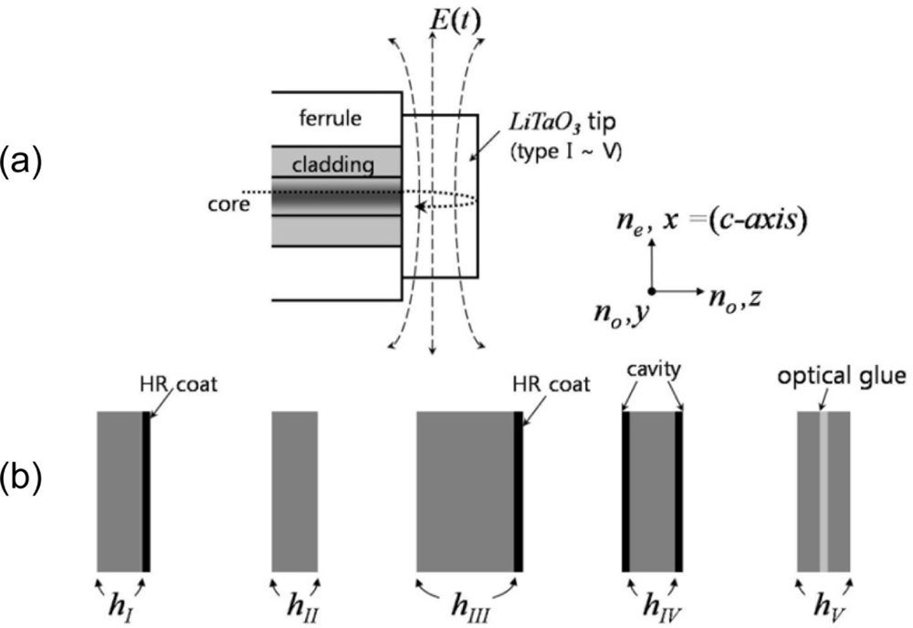
The most distinguishing feature of EO sensors for use in electromagnetic-field detection is their distinctly low-invasiveness compared to common electrical-field probes. For the bulk probes, interference with the signals to be measured or the operation of the device under test can be substantially decreased, and scanning mobility and spatial resolution can be significantly improved, by mounting the sensor crystals on the output facet of an optical fiber [shown in Figure 1(a)]. Various types of tip-on-fiber EO sensors have been reported [7–10,17,18] and we review and compare five distinct types of EO-sensor designs [shown in Figure 1(b)].
2.1. Type I: Conventional Double-Pass Probe
First, we review what is arguably the most common fiber-probe type [7–9]. Here, what is basically a double-pass probe will be called type I. It is based on a retro-reflection process that utilizes a dielectric mirror on the output surface of the probe tip to cause the reflected light to be coupled back along the original fiber path through the tiny fiber core. Such fiber-based EO probes can be categorized into two main sub-types: those that are directly fiber-mounted [7], and those that are attached to a ferrule and GRIN-lens assembly, depending on how the optical beam diverges within the EO crystal [8,9]. The size of the EO crystal is the crucial factor in determining the mounting type, and a clear criterion was presented for this in reference [9]. For thick crystals (up to ∼1 cm), either a quarter- or half-pitch GRIN lens is used to collimate [9] or focus [8] the probe beam onto the sensor plate, respectively. Assembling a probe using a quarter-pitch GRIN lens is generally sufficient to couple the light, but the beam spot becomes maximized at the lens output, while for a half-pitch GRIN the output light is minimized. This is an important design criterion if the spatial resolution of the measured fields is to be optimized.
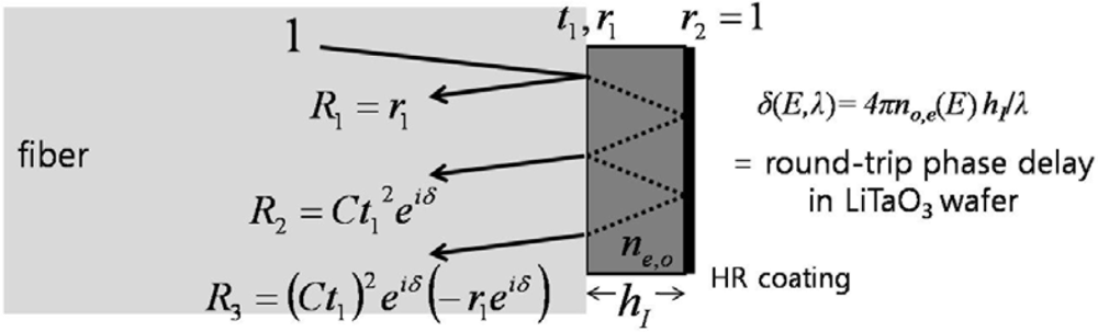
Alternately, crystals up to 1 mm thick can be directly mounted on a thermally-expanded-core fiber-end [7], because the increased numerical aperture of the expanded core allows one to achieve virtually a collimated beam within the crystal volume. As the thickness of a crystal becomes much smaller (to less than 0.1 mm or so), a well-polished fiber ferrule or even a cleaved bare fiber-end is reasonable for capturing the majority of the reflected light. Here, we will concentrate on such a type I probe (i.e., ferrule + thin crystal tip with a mirror), as illustrated in Figure 2. In this figure, a 100 μm thick, x-cut LiTaO3 plate with an HR coat (mirror) on its free surface is mounted directly on the face of a fiber (n ∼1.5). The incident optical beam component through the fiber is partially reflected at the first interface (fiber-LiTaO3) with the Fresnel coefficient r1. The transmitted field component (t1) is then reflected at the second interface (LiTaO3-mirror) with another reflection coefficient r2 ∼1.
The majority of this component is coupled back onto the original fiber path. The magnitude of the coupled component is Ct12r2, where C is a coupling factor associated with the numerical aperture of the fiber and the thickness of the crystal (where C can be maintained at a high value for reasonably thin crystals). This coupled component possesses an additional phase retardation arising from the Pockels effect, given by δ(E,λ) = 4πno,e(E,λ)h/λ and due to the electric (E) fields that the EO crystal experiences.
The EO LiTaO3 crystal is positive uniaxial (i.e., ne > no) and belongs to the symmetry class 3m. Hence, it has two birefringence terms, Δno,e = (ne − no) + (ne3r33 − no3r13)E/2 [19]. The first and second terms are the natural and electrically-induced birefringences, respectively. Δno,e is the term we can control with E fields and polarizations. When the light is linearly polarized along the e-axis (or o-axis), the phase retardation by the crystal is δe(E,λ) = 4πneh/λ + 2πne3r33hE/λ (or δo(E,λ) = 4πnoh/λ − 2πno3r13hE/λ), because the light experiences only one refractive index throughout the crystal. In this case, Δδe(E,λ) = 2πne3r33hE/λ (or Δδo(E,λ) = −2πno3r13hE/λ) controls the E-field-induced phase modulations. Conventional fiber-coupled EO probes sense electric fields in phase modulation forms that are being transformed into amplitude modulations. To realize a conversion to amplitude modulation, additional polarization optics is commonly used to obtain a sine (or cosine)-squared transfer function, created by a pair of crossed polarizers. An optional quarter-wave plate is required if one wishes to shift the operating bias point along the sine-squared curve.
2.2. Type II: Interference Probe
In contrast to the conventional single- or double-pass EO-modulation method, it has been demonstrated that for a system employing an interferometric EO probe (here called type II), the use of polarizers and wave plates within the beam path may actually be avoided [17,20]. The type II EO probe utilizes the slope of its interference fringe along with field-induced EO phase retardations, which are inherently created by the EO crystal itself. In the type-I case, the reflections from the two surfaces of the crystal wafer are highly unbalanced (i.e., r2 ≫r1) due to the mirror, which requires a coating process to produce the last crystal-air interface. In actuality, the two dominant light components—coupled back to the fiber-crystal interface—are r1 + Ct12r2.exp(δ(E,λ)), where δ(E,λ) can be δe or δo depending on the polarization of the light beam. Also, r1 and Ct12r2 can be comparable because r2 (at the crystal-air interface) is always a bit larger than r1 (at the fiber-crystal boundary), and their difference can be compensated by Ct12 which is accordingly smaller than unity if a crystal with proper thickness and refractive index is used.
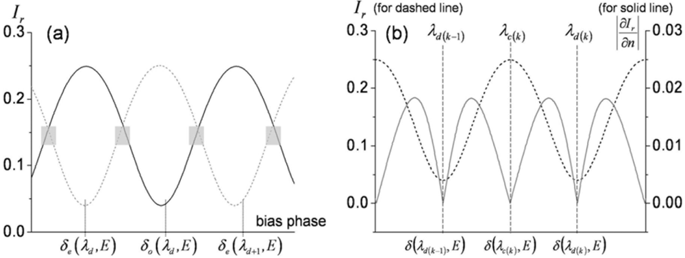
Since the magnitudes of the two interferometric terms are comparable, clear interference fringes are formed within the range of their sum and difference. The period of the fringes is determined by the phase delay term exp(δ(E,λ)) which is significantly affected by polarization and light wavelength. We use a ∼1.55-μm-wavelength distributed feedback (DFB) laser diode, and the known birefringence parameters of the LiTaO3 crystal at 1558 nm are ne = 2.1224, no = 2.1186, r33 = 27.4 (pm/V), and r13 = 6.92 (pm/V) [21]. When a linear beam polarization is set along one of the refractive indices (ne or no) of the LiTaO3, the dominant reflected beam components are r1 + Ct12r2exp(δo,e(E,λ)) (we ignore multi-round trip terms in the crystal, as the first two reflections are dominant). With no exposure to E fields from an electronic source, wavelength and polarization are the only quantities that control the reflectance. Figure 4(a) shows the fringe patterns for a 10 nm span near 1.55 μm. Two distinct fringe patterns exit for linear polarizations aligned along the respective no or ne axis of the LiTaO3 wafer. Although the amount of natural birefringence (ne − no) is minute, such that either refractive index with a crystal of 100 μm thickness would yield approximately a 5.72-nm mode-spacing at this wavelength band, the position of destructive wavelength (λd) could vary substantially, as shown in Figure 4(a). The simulation is done for ideal reflection and coupling conditions (r1: fiber-LiTaO3; r2: LiTaO3-air; C = 1). Such an interference fringe pattern is similar to that of a Mach-Zehnder (MZ) modulator where a DC bias controls the operating point of modulation. Contrary to this, for the type-II interference-based probe, the wavelength serves as the static field bias in the MZ modulators. Setting the spectral biases at the steepest modulation slopes [gray areas in Figure 4(a)], efficient light modulation can be attained by inducing a dynamic phase retardation associated with electric fields. The EO sensitivity is basically proportional to the slope of the fringe pattern. The EO phase modulation (PM) gets transformed to an amplitude modulation (AM) through such a PM-AM conversion curve, and its conversion efficiency slope with respect to the fringe pattern is shown in Figure 4(b).
2.3. Type III: Thick Interference-Based Probe
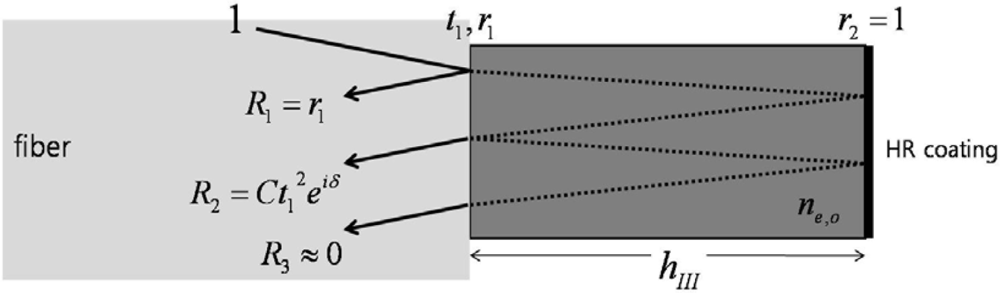
This type of probe can be understood as a hybrid of the type-I and -II probes. As the crystal in a type-II probe becomes thicker, the coupling efficiency C degrades, so that the secondary interference term—which contains important EO-phase-modulation information—becomes less associated with the primary interference term that is reflected at the fiber-crystal interface. In type-I probes, this secondary term is dominant over the first term, so the interference effect is often ignored. In type-II probes, those two terms can be reasonably balanced, and thus the PM component may be converted to AM through an interference process without using a polarizer (or analyzer). In either of the type-I or -II cases, it would be greater to increase the EO interaction length by simply employing a thicker crystal. However, the coupling efficiency C degrades rapidly due to the beam divergence in a thicker crystal.
The reduced coupling efficiency can be compensated by increasing the reflection at the crystal-air interface (r2) via an HR-coated mirror. As an example, for a crystal five times thicker than that in Figure 2, the period of the fringes will shrink accordingly due to the increased cavity length, while the coupling efficiencies are nicely maintained by the HR mirror. This will be verified in the experimental section below.
2.4. Type IV: Resonance Probe
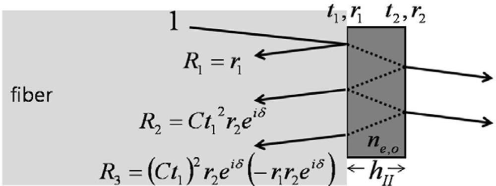
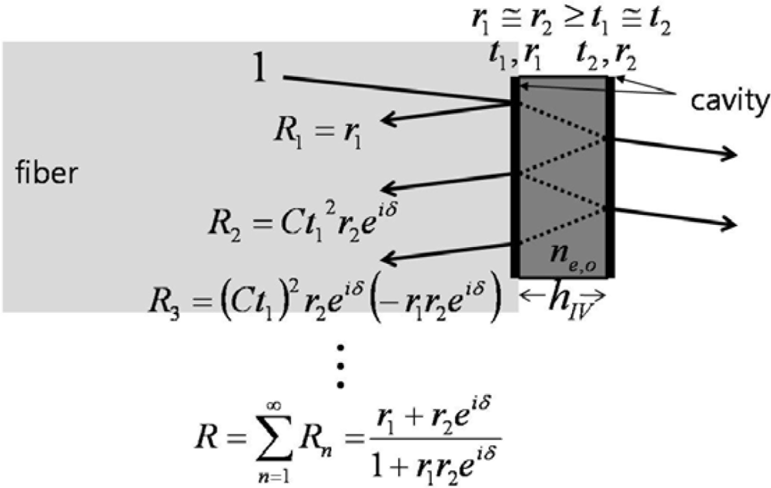
In the first three types of probes, not only does the conventional type-I case use just a single round-trip phase modulation (based on the double pass scheme of the probes), but so too, essentially, do the other two interference-based probes. To enhance the interaction length of the crystal, there have been numerous investigations that utilize a resonance effect [10,22–28]. Building an optical cavity around the crystal, the probing light can be contained for much longer than in the single-round-trip case, and thus resonantly enhanced cumulative phase components can contribute to an improvement in sensitivity. Moreover, the multi-pass components associated with the cavity can also significantly increase the sharpness of the interference fringes (i.e., the finesse of the cavity). Thus, the PM-AM conversion slope becomes more effective, resulting in sensitivity enhancements without increasing the volume of the crystal.
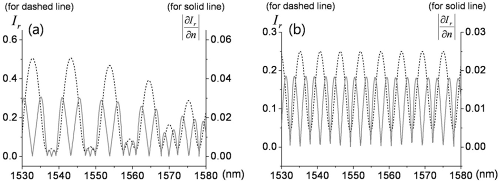
Such resonance-based EO-sensing schemes can be better understood by considering Figure 6. In a cavity that has large reflection coefficients (at least r ≥ t), higher order reflection terms (R3 or higher) may no longer be ignored, but rather must be included to obtain the overall reflection components. The summation of the reflected field components R(E,λ) is (r1+ r2exp(δ(E,λ)))/(1+ r1r2exp(δ(E,λ))), as expressed in Figure 6. Hence, the reflected intensity is Ir(E,λ) = |R(E,λ)|2, which heavily depends on the wavelength and polarization of the light. As discussed for the previous probe types, the input polarization is set parallel to the optic-axis to maximize the EO phase retardation and to only capture the light modulation along the ne axis, while the wavelength bias is set at the point of steepest slope on the spectral fringes. Having fixed these two conditions, the only variable that can change the light intensity is the refractive index of the crystal. Since the EO crystal changes its refractive index with applied E-fields, and the amount of index modulation is typically minute for most EO sensing applications, the sensitivity of the EO amplitude modulation is proportional to ∂Ir(E,λ)/∂n(E). Figure 7 displays the fringe patterns associated with a cavity (r12 = r22= 0.5) and its corresponding EO sensitivity.
2.5. Type V: Multi-Layer Probe
Building a resonator out of the EO crystal has been a significant advancement for overcoming the inherently minute nature of the Pockels effect on the refractive index of the sensor medium, because of the increase in EO interaction length within the sensor. In the type-IV probe, we used a balanced resonator (Fabry-Perot type) to enhance the EO phase retardation and to allow utilization of the steepened modulation slope. Such resonant retardation could be enhanced even more significantly through the use of an unbalanced structure (i.e., of Gires-Tournois type) [25].
A novel design approach was recently presented for realizing another resonance-based, electro-optic-sensing scheme, without relying on highly reflective surfaces [18]. Utilizing two or more uncoated EO wafers, the reflectance resonance characteristics can be improved, and thus the EO phase retardation and the slope of the function responsible for phase-to-amplitude modulation-conversion (which is also associated with the multi-stratified embodiment) are also enhanced.
The multi-layer scheme is basically an extension of the type-II case, in which a single dielectric EO wafer naturally forms a Fabry-Perot etalon, and thus it has unique transmission/reflection characteristics. The transmittance/reflectance of the etalon is slightly modulated as the refractive index of an EO medium is perturbed by an applied E-field. Such EO modulation effects can be enhanced by adding other layers of appropriate thicknesses.
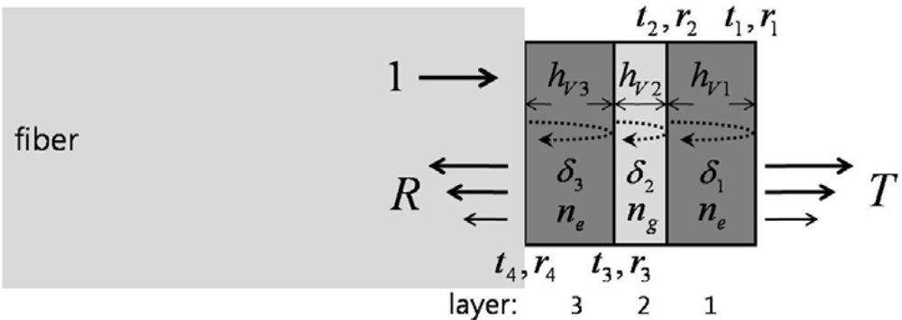
Figure 8 is a schematic of a type-V probe that consists of three stratified layers mounted on a fiber facet. Layers 1 and 3 are x-cut LiTaO3 wafers, and thus both of their optic-axes are perpendicular to the travel of the optical beam. The incoming optical beam is transmitted through a fiber core (ncore ∼1.5), after which it passes through layer 3 (LiTaO3), layer 2 (an optical adhesive with ng ∼1.5), and layer 1 (identical to layer 3). The overall optical field transmission from such a three-layer system is expressed in Equation 1 based on the transfer function and standard feedback theory [18,29]:
where the first-order feedback terms are: −(r1r2eiδ1 + r2r3eiδ2 + r3r4eiδ3)
the second-order feedback terms are: −(r1r3ei(δ1+δ2) + r2r4ei(δ2+δ3) + r1r2r3r4ei(δ1+δ3))
and the third-order feedback terms are: −(r4r1ei(δ1+δ2+δ3))
For overall reflectance, we may utilize the complementary relation: Ir = |R|2 = 1 − |T|2 = 1 − It for lossless media. The simulated reflectance of this type-V probe for 50-μm-thick EO wafers (layer 1, 3: ne = 2.1224) and a 10-μm-thick adhesive gap (layer 2: ng = 1.5) is shown in Figure 9. The polarization of the laser was assumed to be linear along the x-direction (extra-ordinary axis) as in previous probe types.
The spectral range chosen was centered at ∼1.55 μm, with a span wide enough to explore complex interferometric fringe relations. The fringes in Figure 9 consist of fine and wide periodic patterns, which are determined by δ1 (or δ3) and δ2, respectively. The steeper slope of the reflected-intensity fringes over a broad spectral region is advantageous for efficient EO amplitude modulation. This condition can be achieved by reducing the gap between wafers or by using a gap-medium of lower index. As in previous interference or resonance probes, the sensitivity of the EO amplitude modulation versus a minute E-field-induced index, is proportional to ∂Ir(E,λ)/∂n(E). Since It (E,λ) + Ir (E,λ) = 1 − loss(λ), the sensitivity becomes ∂Ir/∂n = −∂It/∂n, where n is an electro-optical variable (here, n = n1 = n3 = ne). The partial derivative of intensity over the variable index can be readily obtained by numerically perturbing refractive index terms. It should be noted that this approach also inherently deals with resonance-based phase-enhancement terms as described in references [23] and [24].
The reflectance and corresponding EO sensitivity within the wavelength region appropriate to optical-communication sources are computed for 0.01% modulation of ne, and shown in Figure 10. Figure 10(a) indicates the normalized EO sensitivity compared to the slopes of the reflectance with the simulation parameters as in Figure 9. However, as we remove the gap between the EO wafers (that is h1 = 100 μm, h2 = h3 = 0), the slope of the fringe is reduced, as observed with the correspondingly reduced EO sensitivity in Figure 4(b).
3. Performance Evaluation of Fiber-Coupled EO Probes
The set of five probes described above was fabricated in order to conduct an experimental evaluation of their performance. For the conventional, type-I probe, we used a 100 ± 5-μm-thick, x-cut LiTaO3 plate with a 99% HR-coated mirror. Practically, considering non-ideal coupling conditions (C < 1) and minor spectral ripples associated with small reflections at the fiber-LiTaO3 interface, the coupled light is typically about two thirds of the input power. Since its spectral slope for effective PM-AM conversion is relatively weak, an additional polarization controller and analyzer were employed just before the photodetector. Here, an analyzer creates the well-known sine-squared PM-AM conversion slope of a single-pass EO modulator, and the second polarization controller adjusts the EO modulation bias. We also made a type-II probe using the same material and procedure, except that the HR mirror was not included.
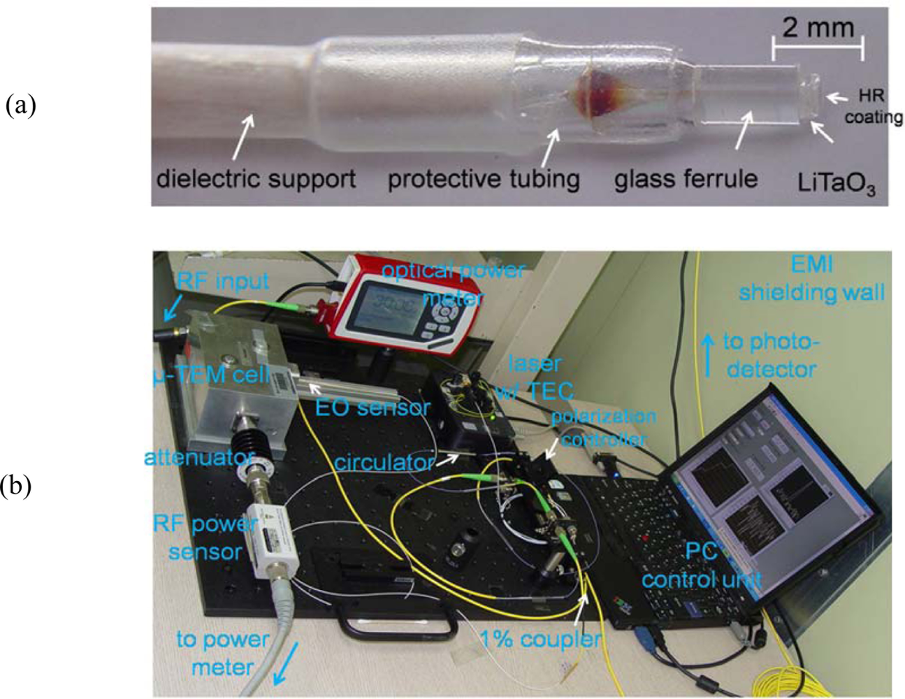
Using a LiTaO3 plate five times thicker than the EO medium of the type-I probe (500 ± 5 μm), a type-III probe was fabricated. A type-IV probe, intended as an improved version of the type II case, was also produced, with a balanced cavity added to the faces of the EO plate. A type-V probe was assembled based on the proposed three-layer configuration in Figure 8. The thickness of each LiTaO3 wafer used here was 50 ± 5 μm, and a narrow gap between the two wafers was filled with UV-curing cement. The wafer stack was pressed together in order to minimize the gap between the EO wafers to ∼2 μm.
To utilize the slopes of the spectral reflection fringes in each probe (types II–V), the laser has to cover sufficient wavelength tuning ranges. It would be ideal to use a widely tunable laser source, such as an external-cavity diode laser. However, a commercial optical-communication-grade distributed-feedback (DFB) laser diode can replace the more expensive tunable sources, since a DFB laser exhibits limited tunability via thermo-electric control (TEC). A typical DFB laser diode in the 1.5-μm wavelength band readily covers a few nm of tuning range using such thermal control. The relationship of laser wavelength and temperature control reported previously, where ∼2.5 nm of tuning range was attained by 30 degrees of dynamic temperature control, was again employed in this study [17].
For all of the probes of type II through V, the slopes of the spectral reflection fringes are used in order to perform EO sensing. It is apparent that controlling the wavelength bias (by the laser-diode temperature setting) at the steepest slopes of the fringes yields the strongest EO signal for each probe. However, from a practical perspective, it has been found that it is advantageous to lower the bias to achieve a better signal-to-noise ratio (SNR) [30-35]. This is because the noise level is primarily proportional to the laser power level that a detector receives. Lowering the wavelength bias reduces the light intensity more than the gradient of the fringes. Straightforward modeling and experimental analysis of bias optimization for SNR enhancement can be found in reference [35]. A closer look at the low-bias points for each probe in Figure 11 is presented in Figure 12, where the incident laser power to the probes is 30 mW, and the 10% reflectance level was used for the respective bias point of each probe. The saturation power level of our photodiode is ∼3 mW, and ∼2.8 mW of EO-sensing probe beam is coupled to a photodiode through a circulator. Receiving the same power, the noise level of the photodiode for each probe becomes comparable, whereas the signal strength heavily depends on the slope of the fringes and the interaction length of the crystal. The overall reflectance of each probe (type II–V), measured over 2.5 nm of spectral range, is shown in Figure 11. The polarization of the laser was set along the ne axis of the LiTaO3 wafers, so as to have clean interferometric fringes, as well as maximized EO phase retardation.
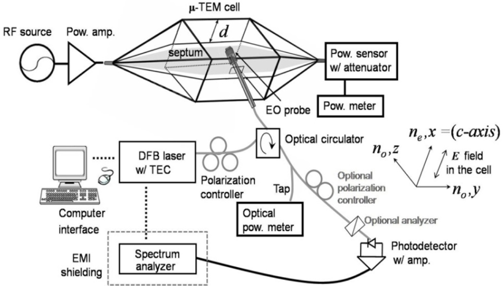
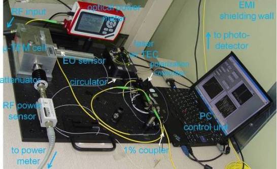
The sensitivity of each EO probe can be evaluated if one uses a calculable, and thus known electric-field strength from a standard field-generating device. One excellent choice for such field strength calibration is a micro-transverse-electromagnetic (μ-TEM) cell, where the reference field strength can be calculated with low uncertainty from parameters of the cell such as the reflection coefficient, input power, and geometrical dimensions [36–38]. The field strength inside the cell is proportional to the input power and inversely proportion to the septum (center conductor) distance of the cell. The μ-TEM cell has a very small septum height (d in Figure 13) compared to a conventional TEM cell, and therefore it can generate a relatively high E-field for the same input power level. The electric fields are linearly polarized in a vertical direction in the TEM cell and are uniform in the useable test area, which is located in the center region between the septum and the upper wall of the cell. To sense these fields, the EO probe end was placed at the precise center of the test area through a tiny hole in the side wall. The optic-axis of the sensor is parallel to the E-fields (x-direction in Figure 13) in order to maximize the sensing fields.
The complete probe-evaluation system is illustrated in Figure 13, and a photograph of the actual layout appears in Figure 14.
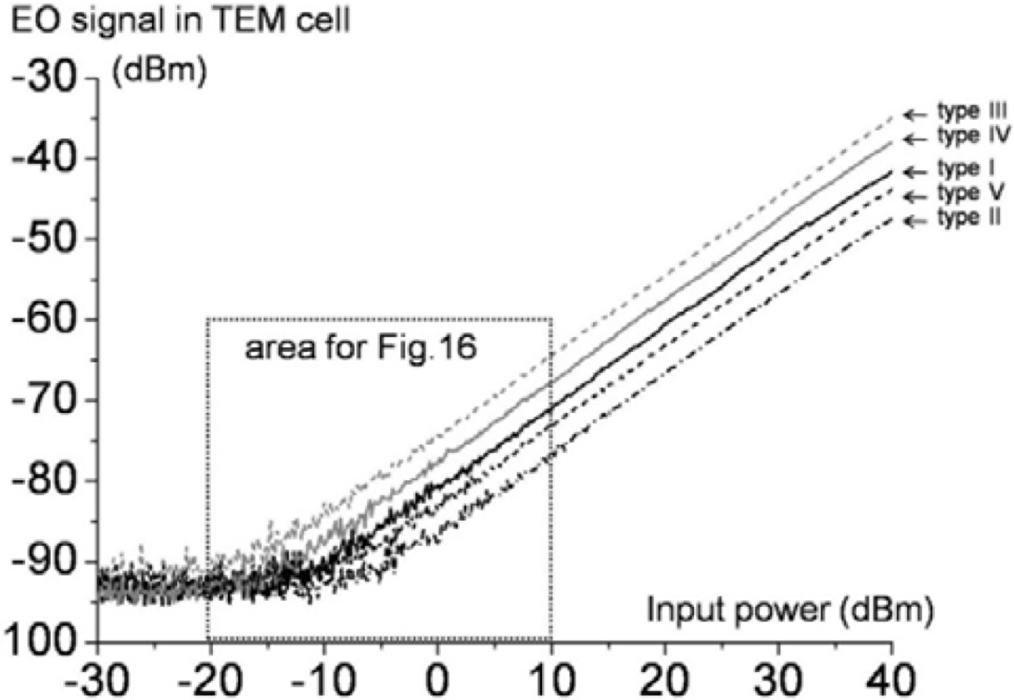
A fiber-pigtailed diode laser, manual polarization controller, optical circulator, and fiber-connectorized photodiode were spliced together with the probe to form a continuous, low loss, enclosed optical path. The 30 mW of polarization-controlled light flows to the probe-head tip, and the known electric field and the optical beam intersect within the EO medium. The reflected/modulated beam—which contains the valuable information on the amplitude and phase of the electric fields—is routed to the photodetector so that the field components may be demodulated. The SNR performance of such electrical-signal measurements is evaluated using an electrical spectrum analyzer. The μ-TEM cell has broad bandwidth (DC∼1 GHz), and we fed up to +40 dBm of power into the cell at 1 GHz in order to evaluate the high-power-handling capability, linearity, and dynamic range of each probe (type I–V).
The probe-evaluation system requires a second polarization controller and analyzer in the optical beam path before the photodetector for the type-I probe configuration. In conventional type-I sensing, typically the operating bias is set so that the light output is 50% of the input intensity, or at a position of half the maximum value on the sine-squared AM curve. However, similar to the type II-V cases, lowering the bias to a point close to the null output of the modulator is advantageous for SNR, due to the fact that the noise will be suppressed by a greater amount than the signal at this point [30–35]. Maintaining the reflected power from the probe at the same 10% level, the signal level was then maximized by adjusting the two polarization controllers.
Compared to previous publications [17,18], an additional preamplifier was used to boost the signal level while significantly lowering the noise level (by ∼15 dB) through shielding of the read-out instrument from electromagnetic interference (EMI). Each signal plot maintains its linearity up to +40 dBm of TEM-cell input power without probe damage or any indication of saturation. Since the EO sensor has an all-dielectric embodiment, it should be able to sense even higher RF power. To investigate the minimum detectable electric fields for the different probes, the detail of Figure 15 at weak RF driving power is considered in Figure 16. By measuring these calculable fields in the standard TEM cell with an EO probe, the EO signal levels can be mapped onto the corresponding absolute field strengths in V/m. The absolute electric field strength within the cell’s test area between the upper wall and the septum (i.e., the septum height) is determined by the equation (PZo)1/2/d (in V/m), where P is the net power flowing through the cell, Zo is the complex characteristic impedance of the cell, and d is the septum distance [36–38].
Our cell features yield Zo = 50.319 Ω and d = 34.405 mm, and thus by measuring the P values versus input power, the calculated absolute electric fields in the test area of the cell can be attained (see the solid curve in Figure 16). For instance, the minimum detectable field of the type III probe (dashed gray line) is determined to be between 1–2 V/m. At −10 dBm of cell power, an EO signal level of ∼6 dB above the upper peak noise level is found. This signal level corresponds to 2 V/m by correspondence to the electric-field plot (solid, curved line). It should be noted that each signal curve is the trace of the peak values on the signal spectra, so the noisy portion along each signal trace is the upper limit of the experiment’s noise floor. The actual average noise floor is ∼−95 dBm ± 5 dB, so the minimum detectable field strength is practically very close to the 1 V/m level. This condition can be achieved averaging the noise level with a longer sweep time on a spectrum analyzer.
The stability of the sensors is an important factor in instances where a long-term measurement is required—for instance, due to the fact that the sensitivities of probe types II–V are all temperature-dependent. Potential temperature drift can be overcome through the use of a TEC-locked loop, which employs feedback so that the wavelength needed for optimal EO sensitivity can be held constant during the entire measurement time. In addition, if one wishes to translate the probes to sense the field at different locations, the light polarization inside the optical fiber should be fixed to insure consistent and optimal operation of the probes. This challenge may be overcome by using polarization-maintaining fibers.
The characteristics of each probe type are summarized in Table 1. The physical operating principle, sensitivity, probe coating, and analyzer requirements have been discussed throughout the text. In regards to fabrication difficulty, the efficient coupling of the reflected beam from the probe crystal back into the optical fiber is the main issue. Probe types I–III are reasonably straightforward to assemble, as these utilize only single round-trip phase-delay components from the crystal. On the contrary, since type-IV probes need to couple multiple round-trip components, and type-V probes utilize sophisticated reflection components resulting from multi-layer coatings, their fabrication is significantly more challenging.
Low invasiveness is one of the distinguishing features of EO sensors. The sensor volume that interacts with the E-fields to be measured is a key factor in the invasiveness. For the same sensor volume, the invasiveness of type I, II, and IV probes would be relatively small, since the dielectric optical coating is negligibly thin. The invasiveness increases slightly as the crystals become larger (type III) and/or more complex (type V).
The bandwidth of the sensors is determined by the optical interaction length of the sensor crystal. In case of our type I and II sensors (100 μm, LiTaO3), the single round trip optical propagation time is 1.43 ps. Although such delays may be multiplied several times for thicker crystals (e.g., type III) or for longer interaction lengths within cavities (type IV) or periodic structures (type V), the delay should not impact the sensing of microwave fields having the longer temporal periods (e.g., 1 GHz corresponds to a period of 1 ns) examined in these experiments. The bandwidth of the EO crystals themselves is known to extend well into the THz regime [39], so the actual bandwidth of the EO-sensing technique is determined primarily by the probe structure, and secondarily by the capabilities of the high-speed light modulation and detection.
Besides the low invasiveness of the sensors, EO probing is particularly well-suited for high-voltage or high-power microwave applications [40]. In our TEM cell, the max field is 652 V/m at + 40 dBm input power, while the damage level of the all-dielectric EO sensor is known to be on the order of 1 MV/m [40]. We expect these types of probes to have an extremely wide, nearly 120 dB (V/m-MV/m) dynamic range. As the probe handles kV/m-MV/m scales of intense fields, the light would be highly modulated, as much as in a typical electro-optic modulator. Such super intense field information would be readily demodulated using mature optical-telecommunications detection techniques.
4. Conclusions
We have reviewed five types of fully dielectric and fiber-coupled electro-optic sensors for non-destructive microwave field detection. The structures and operation principles of conventional double-pass, interference, thick-interference, resonance and multi-layer probes are presented in detail. The performance of each probe is compared by measuring the absolute electric fields with a huge dynamic range. Each type shows pros and cons in various aspects such as sensitivity, cost, invasiveness and sensing speed. The design scheme and performance comparison of each probe can serve as a good guideline for low-invasive and high-power-handling electro-optic sensing applications.
Acknowledgments
This material is based upon work supported by the Korea Research Institute of Standards and Science (KRISS) and Agency for Defense Development (ADD).
References
- Valdmanis, J.A.; Mourou, G.A. Subpicosecond electro-optic sampling: Principles and applications. IEEE J. Quantum Electron 1986, 22, 69–78. [Google Scholar]
- Valdmanis, J.A. 1 THz-bandwidth prober for high speed devices and integrated circuits. Electron. Lett 1987, 23, 1308–1310. [Google Scholar]
- Shinagawa, M.; Nagatsuma, T. An automated electro-optic probing system for ultra-high-speed IC’s. IEEE Trans. Instrum. Meas 1994, 43, 843–847. [Google Scholar]
- Yang, K.; David, G.; Robertson, S.; Whitaker, J.F.; Katehi, L.P.B. Electro-optic mapping of near-field distributions in integrated microwave circuits. IEEE Trans. Microwave Theory Tech 1998, 46, 2338–2343. [Google Scholar]
- Yang, K.; Yook, J.G.; Katehi, L.P.B; Whitaker, J.F. Electrooptic mapping and finite-element modeling of the near-field pattern of a microstrip patch antenna. IEEE Trans. Microwave Theory Tech 2000, 48, 288–294. [Google Scholar]
- Nagatsuma, T. Photonic measurement technologies for high-speed electronics. Meas. Sci. Technol 2002, 13, 1655–1663. [Google Scholar]
- Wakana, S.; Ohara, T.; Abe, M.; Yamazaki, E.; Kishi, M.; Tsuchiya, M. Fiber-edge electrooptic/magnetooptic probe for spectral-domain analysis of electromagnetic field. IEEE Trans. Microwave Theory Tech 2000, 48, 2611–2616. [Google Scholar]
- Yang, K.; Katehi, L.P.B; Whitaker, J.F. Electric field mapping system using an optical-fiber-based electro optic probe. IEEE Microw. Wireless Compon. Lett 2001, 11, 164–166. [Google Scholar]
- Togo, H.; Shimizu, N; Nagatsuma, T. Near-field mapping system using fiber-based electro-optic probe for specific absorption rate measurement. IEICE Trans. Electron 2007, E90–C, 436–442. [Google Scholar]
- Lee, D.J.; Crites, M.H.; Whitaker, J.F. Electro-optic probing of microwave fields using a wavelength-tunable modulation depth. IOP Meas. Sci. Tech 2008, 19, 115301–115310. [Google Scholar]
- Yang, K.; Katehi, L.P.B; Whitaker, J.F. Electro-optic field mapping system utilizing external gallium arsenide probes. Appl. Phys. Lett 2000, 77, 486–488. [Google Scholar]
- Yang, K.; Marshall, T.; Forman, M.; Hubert, J.; Mirth, L.; Popovic, Z.; Katehi, L.P.B; Whitaker, J.F. Active-amplifier-array diagnostics using high-resolution electrooptic field mapping. IEEE Trans. Microwave Theory Tech 2001, 49, 849–857. [Google Scholar]
- Kuo, W.K.; Pai, C.H.; Huang, S.L.; Chou, H.Y.; Huang, H.S. Electro-optic mapping systems of electric-field using CW laser diodes. Opt. Laser Technol 2006, 38, 111–116. [Google Scholar]
- Sasagawa, K.; Kanno, A.; Kawanishi, T.; Tsuchiya, M. Live electrooptic imaging system based on ultraparallel photonic heterodyne for microwave near-fields. IEEE Trans. Microwave Theory Tech 2007, 55, 2782–2791. [Google Scholar]
- Chen, C.C.; Whitaker, J.F. An optically-interrogated microwave-poynting-vector sensor using cadmium manganese telluride. Opt. Express 2010, 18, 12239–12248. [Google Scholar]
- Chandani, S.M. Fiber-based probe for electrooptic sampling. IEEE Photon. Technol. Lett 2006, 18, 1290–1292. [Google Scholar]
- Lee, D.J.; Kang, N.W.; Kwon, J.Y.; Kang, T.W. Field-calibrated electro-optic probe using interferometric modulations. J. Opt. Soc. Am. B 2010, 27, 318–322. [Google Scholar]
- Lee, D.J.; Kwon, J.Y.; Ryu, H.Y.; Whitaker, J.F. A multi-layer electro-optic field probe. Opt. Express 2010, 18, 24735–24744. [Google Scholar]
- Yariv, A.; Yeh, P. Optical Waves in Crystals; Wiley: New York, NY, USA, 1984; Chapter 8. [Google Scholar]
- Lee, D.J.; Whitaker, J.F. A simplified Fabry—Pérot electrooptic-modulation sensor. IEEE Phot. Tech. Lett 2008, 20, 866–868. [Google Scholar]
- Casson, J.L.; Gahagan, K.T.; Scrymgeour, D.A.; Jain, R.K.; Robinson, J.M.; Gopalan, V.; Sander, R.K. Electro-optic coefficients of lithium tantalate at near-infrared wavelengths. J. Opt. Soc. Am. B 2004, 21, 1948–1952. [Google Scholar]
- Quang, D.L.; Erasme, D.; Huyart, B. Fabry-Perot enhanced real-time electro-optic probing of MMICs. Electron. Lett 1993, 29, 498–499. [Google Scholar]
- Vickers, A.J.; Tesser, R.; Dudley, R.; Hassan, M.A. Fabry-Perot enhancement electro-optic sampling. Opt. Quantum Electron 1997, 29, 661–669. [Google Scholar]
- Mueller, P.O.; Alleston, S.B.; Vickers, A.J.; Erasme, D. An external electrooptic sampling technique based on the Fabry-Perot effect. IEEE J. Quantum Electron 1999, 35, 7–11. [Google Scholar]
- Mitrofanov, O.; Gasparyan, A.; Pfeiffer, L.N.; West, K.W. Electro-optic effect in an unbalanced AlGaAs/GaAs microresonator. Appl. Phys. Lett 2005, 86, 202103:1–202103:3. [Google Scholar]
- Mitrofanov, O. Terahertz near-field electro-optic probe based on a microresonator. Appl. Phys. Lett 2006, 88, 091118:1–091118:3. [Google Scholar]
- Sasagawa, K.; Tsuchiya, M. An electrooptic sensor with sub-millivolt sensitivity using a nonlinear optical disk resonator. Microwave Phot 2005, 12, 355–358. [Google Scholar]
- Kuo, W.K.; Wu, P.Y.; Lee, C.C. A Fabry—Pérot electro-optic sensing system using a drive-current-tuned wavelength laser diode. Rev. Sci. Instrum 2010, 81, 053107:1–053107:4. [Google Scholar]
- Lee, D.J.; Whitaker, J.F. Analysis of optical and terahertz multilayer systems using microwave and feedback theory. Microwave Opt. Tech. Lett 2009, 51, 1308–1312. [Google Scholar]
- Mitrofanov, O. Laser excess noise reduction in optical phase-shift measurements. Appl. Opt 2003, 42, 2527–2531. [Google Scholar]
- Mitani, S.; Yamazaki, E.; Kishi, M.; Tsuchiya, M. EDFA-enhanced sensitivity of RF magneto-optical probe. Proceedings of International Topical Meeting on Microwave Photonics, Budapest, Hungary, 10–12 September 2003; pp. 255–258.
- Wakana, S.; Yamazaki, E.; Mitani, S.; Park, H.; Iwanami, M.; Hoshino, S.; Kishi, M.; Tsuchiya, M. Performance evaluation of fiber-edge magnetooptic probe. J. Lightwave Technol 2003, 21, 3292–3299. [Google Scholar]
- Sasagawa, K.; Tsuchiya, M.; Izutsu, M. Sensitivity enhancement of electrooptic probing based on photonic downconversion by sideband management. Proceedings of Conference on Lasers and Electro-Optics, Baltimore, MD, USA, 22–27 May 2005; pp. 1185–1187.
- Sasagawa, K.; Tsuchiya, M. Modulation depth enhancement for highly sensitive electro-optic RF near-field measurement. Electron. Lett 2006, 42, 1357–1358. [Google Scholar]
- Lee, D.J.; Whitaker, J.F. Optimization of sideband modulation in optical-heterodyne-down-mixed electro-optic sensing. Appl. Opt 2009, 48, 1583–1590. [Google Scholar]
- Berger, J.; Petermann, K.; Fahling, H.; Wust, P. Calibrated electro-optic E-field sensors for hyperthermia applications. Phys. Med. Biol 2001, 46, 399–411. [Google Scholar]
- Kang, N.W.; Kang, J.S.; Kim, D.C.; Kim, J.H.; Lee, J.G. Characterization method of electric field probe by using transfer standard in GTEM cell. IEEE Trans. Instrum. Meas 2009, 58, 1109–1113. [Google Scholar]
- Crawford, M.L. Generation of standard electromagnetic fields using TEM transmission cells. IEEE Trans. Electromag. Compat 1974, 16, 189–195. [Google Scholar]
- Jiang, Z.; Zhang, X.C. Terahertz imaging via electrooptic effect. IEEE Trans. Microwave Theory 1999, 47, 2644–2650. [Google Scholar]
- Garzarella, A.; Qadri, S.B.; Wu, D.H. Optimal electro-optic sensor configuration for phase noise limited, remote field sensing applications. Appl. Phys. Lett 2009, 94, 221113:1–221113:3. [Google Scholar]


| Probe type | Probe name | Sensitivity | Fabrication difficulty | Need for coating | Need for analyzer | Invasiveness | Temporal resolution |
|---|---|---|---|---|---|---|---|
| I | conventional | good | easy | once | yes | excellent | excellent |
| II | interference | fair | easy | no | no | excellent | excellent |
| III | thick-interference | excellent | easy | once | no | fair | good |
| IV | resonance | excellent | medium | twice | no | excellent | good |
| V | multi-layer | good | hard | no | no | good | good |
© 2011 by the authors; licensee MDPI, Basel, Switzerland. This article is an open access article distributed under the terms and conditions of the Creative Commons Attribution license (http://creativecommons.org/licenses/by/3.0/).
Share and Cite
Lee, D.-J.; Kang, N.-W.; Choi, J.-H.; Kim, J.; Whitaker, J.F. Recent Advances in the Design of Electro-Optic Sensors for Minimally Destructive Microwave Field Probing. Sensors 2011, 11, 806-824. https://doi.org/10.3390/s110100806
Lee D-J, Kang N-W, Choi J-H, Kim J, Whitaker JF. Recent Advances in the Design of Electro-Optic Sensors for Minimally Destructive Microwave Field Probing. Sensors. 2011; 11(1):806-824. https://doi.org/10.3390/s110100806
Chicago/Turabian StyleLee, Dong-Joon, No-Weon Kang, Jun-Ho Choi, Junyeon Kim, and John F. Whitaker. 2011. "Recent Advances in the Design of Electro-Optic Sensors for Minimally Destructive Microwave Field Probing" Sensors 11, no. 1: 806-824. https://doi.org/10.3390/s110100806