Photo-Detectors for Time of Flight Positron Emission Tomography (ToF-PET)

Abstract
: We present the most recent advances in photo-detector design employed in time of flight positron emission tomography (ToF-PET). PET is a molecular imaging modality that collects pairs of coincident (temporally correlated) annihilation photons emitted from the patient body. The annihilation photon detector typically comprises a scintillation crystal coupled to a fast photo-detector. ToF information provides better localization of the annihilation event along the line formed by each detector pair, resulting in an overall improvement in signal to noise ratio (SNR) of the reconstructed image. Apart from the demand for high luminosity and fast decay time of the scintillation crystal, proper design and selection of the photo-detector and methods for arrival time pick-off are a prerequisite for achieving excellent time resolution required for ToF-PET. We review the two types of photo-detectors used in ToF-PET: photomultiplier tubes (PMTs) and silicon photo-multipliers (SiPMs) with a special focus on SiPMs.1. Introduction
Recent advances in the field of medical imaging have greatly facilitated the transition from technologies used to accurately image structures inside the human body to technologies sensitive enough to provide functional and biological information at the cellular and the molecular level. Positron emission tomography (PET) is considered to be one of the most sensitive in-vivo molecular imaging modalities despite its significantly inferior spatial resolution compared to imaging modalities such as computed tomography (CT) and magnetic resonance imaging (MRI). The improvement of PET detector technology is an active field of research and efforts are focused on addressing the limits in spatial resolution and sensitivity achieved in PET.
1.1. Positron emission tomography (PET): Basic principles
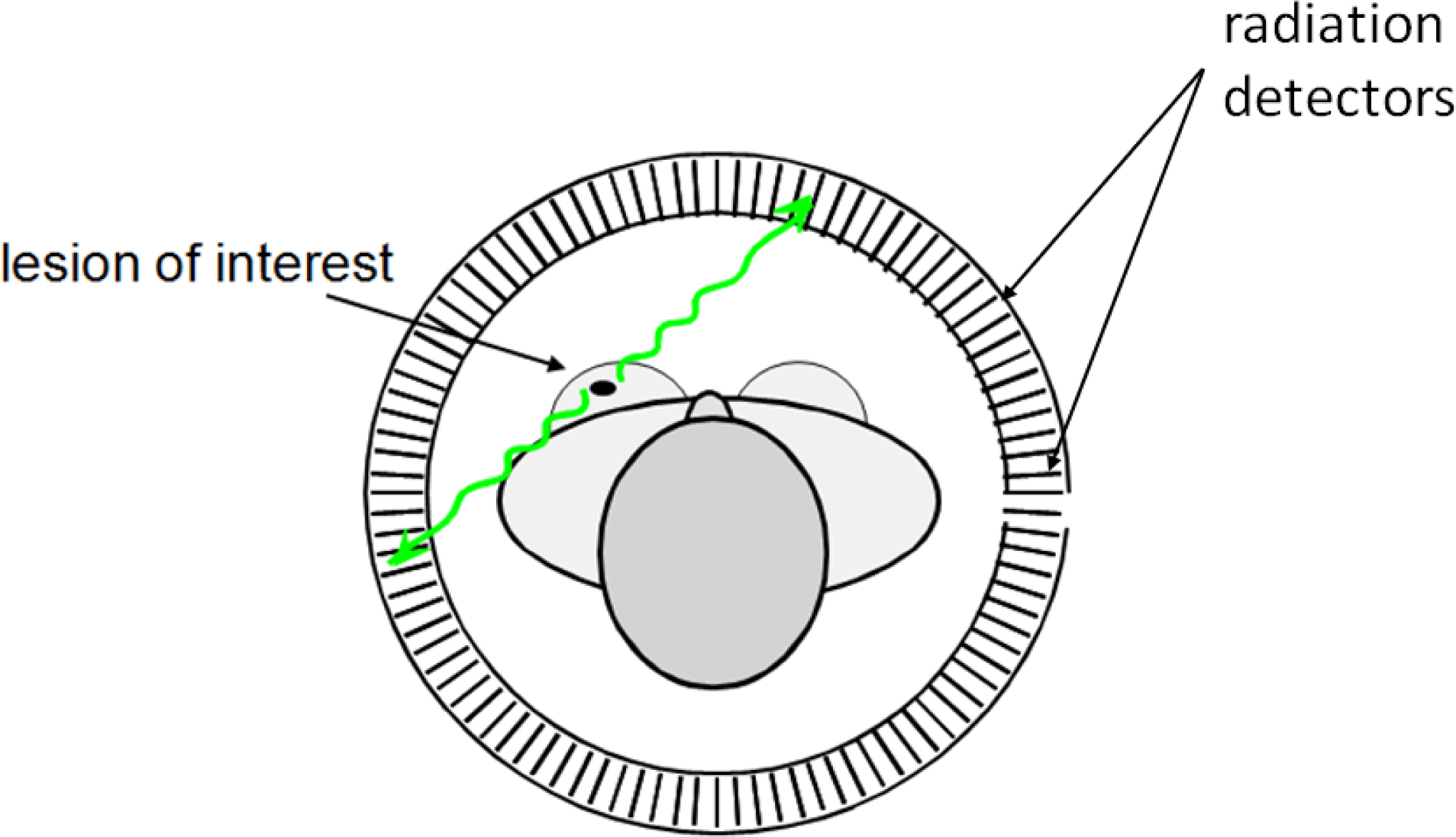
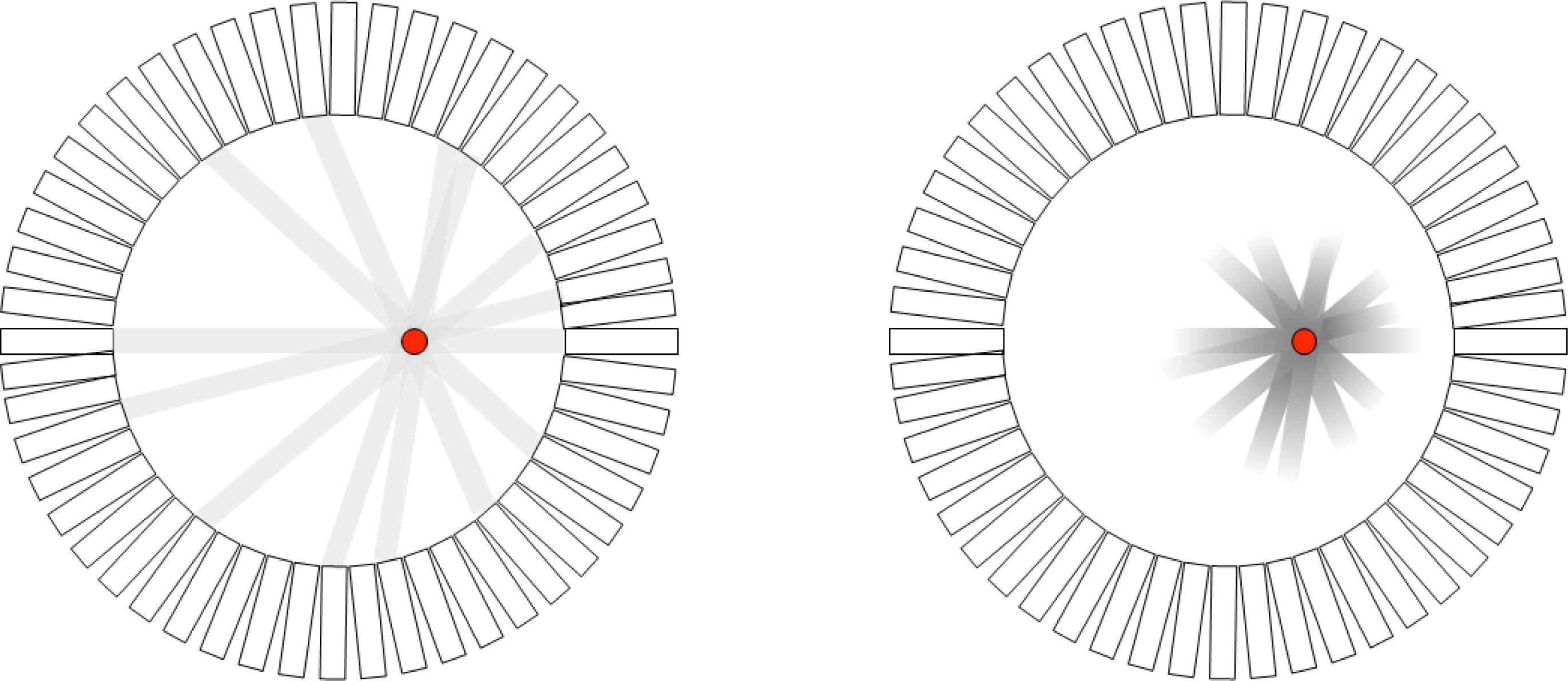
PET imaging is performed after the administration to the patient of a radio-tracer, namely a biomolecule labeled with a radioactive atom emitting positrons (β+ particles). The biomolecule is chosen such that it will preferentially accumulate in the area of interest resulting in high radio-tracer concentration in this region. A PET acquisition is based on the coincident detection of many pairs of simultaneous anti-parallel photons following the annihilation of the positron emitted by the radio-tracer [1]. The detection is performed by a number of detector element pairs which are placed around the imaged object, typically in a ring geometry, as shown in Figure 1. The incident annihilation photons will interact with these detectors which will fully or partially absorb the photon energy resulting in the generation of an electrical signal. This process will be henceforth referred to as a photon event. A PET acquisition will eventually result in a number of identified detector pairs that have simultaneously detected the two annihilation photons, or otherwise stated, the positron annihilation event. These pairs will be subsequently assigned a virtual line connecting the two detection points (line of response, LoR). For every stimulated detector pair the related positron annihilation is localized somewhere along the respective LoR through the patient with no further information about the exact point of positron annihilation along that line. Acquisition from detector pairs at various angular views (tomographic acquisition) followed by appropriate reconstruction algorithms allows for estimation of the tracer biodistribution within the imaged object with a finite spatial resolution and sensitivity.
PET detectors are required to have fast response due to the requirement for detection of simultaneous photon events. To date the detectors typically used in PET have a finite time resolution of a few nanoseconds (ns) allowing for detection of photon events within a predefined time window. The width of this window is usually chosen to be twice the time resolution of the PET detectors.
1.2. The time of flight (ToF) feature: Benefits and challenges
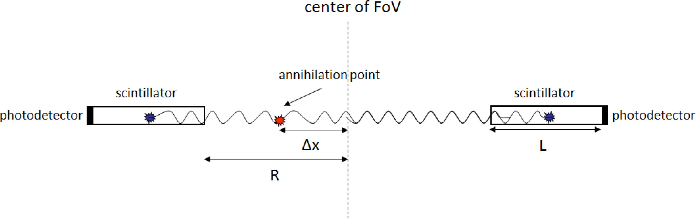
Time of flight PET (ToF-PET) is an advance over traditional PET that exploits the time difference Δt in detection of the two photon events and correlates it to the position Δx of the annihilation point with respect to the center of the field of view (FoV) according to the formula (Figure 2) [2]:
Due to the limited time resolution of the PET detectors the registered time difference Δt is blurred by a variance resulting in a corresponding blurring in the estimated position Δx by a variance (Gaussian structure in Figure 3).
To date the time resolution of PET detectors is not adequate in order for ToF information to be used for exact localization of the annihilation point along the LoR. For example, a detector time resolution of 500 picoseconds (ps) will result in a position blurring of 7.5 cm. This blurring is an order of magnitude higher compared to the spatial resolution of several mm achieved by current clinical PET systems [4] and dominated by the scintillation crystal pixel size [5]. However, time resolution values of hundreds of ps that current detectors have can result in a considerable gain in signal-to-noise ratio (SNR) in the reconstructed image which further implies better lesion detectability, reduced radioactive dose received by the patient and/or reduced scan time [6–8]. An illustration of the difference between a standard PET and a ToF-PET acquisition is illustrated in Figure 4.
1.3. The concept of time resolution
We define the time resolution of a detector as the minimum time interval between two subsequent photon events in order for these to be recorded as separate events [9]. In PET, time resolution is typically measured for pairs of detectors that detect many annihilation photon events and is defined as the full width at half maximum (FWHM) of the distribution of time difference between the two detectors, over multiple events. Typical time resolutions achieved by modern PET systems lie within the 2–10 ns range. In the case of ToF-PET, however, such magnitudes are insufficient in order for ToF information to have a benefit over a conventional PET acquisition. The existing commercially available ToF-PET imaging systems can achieve time resolutions in the range of 500–900 ps allowing for a Gaussian weighted localization with a FWHM of 7.5–13.5 cm along each LoR.
The lowest limit in time resolution for a single photon event that can be achieved is theoretically described by a number of empirical formulas [10,11] and for a generic detector with finite signal-to-noise ratio and transit time jitter could be summarized as follows:
Even though there have been several studies in the past demonstrating the feasibility of ToF PET, only the past few years has it managed to gain popularity in both industry and research. Recent technological advances have led to the development of new scintillator materials and novel photo-detector architectures with improved performance properties that have significantly facilitated the rapid integration of ToF technology into complete imaging systems. In the following, we review the most important components of ToF-PET radiation detectors with emphasis in solid-state photo-detectors.
2. Radiation Detectors for Fast Timing Applications
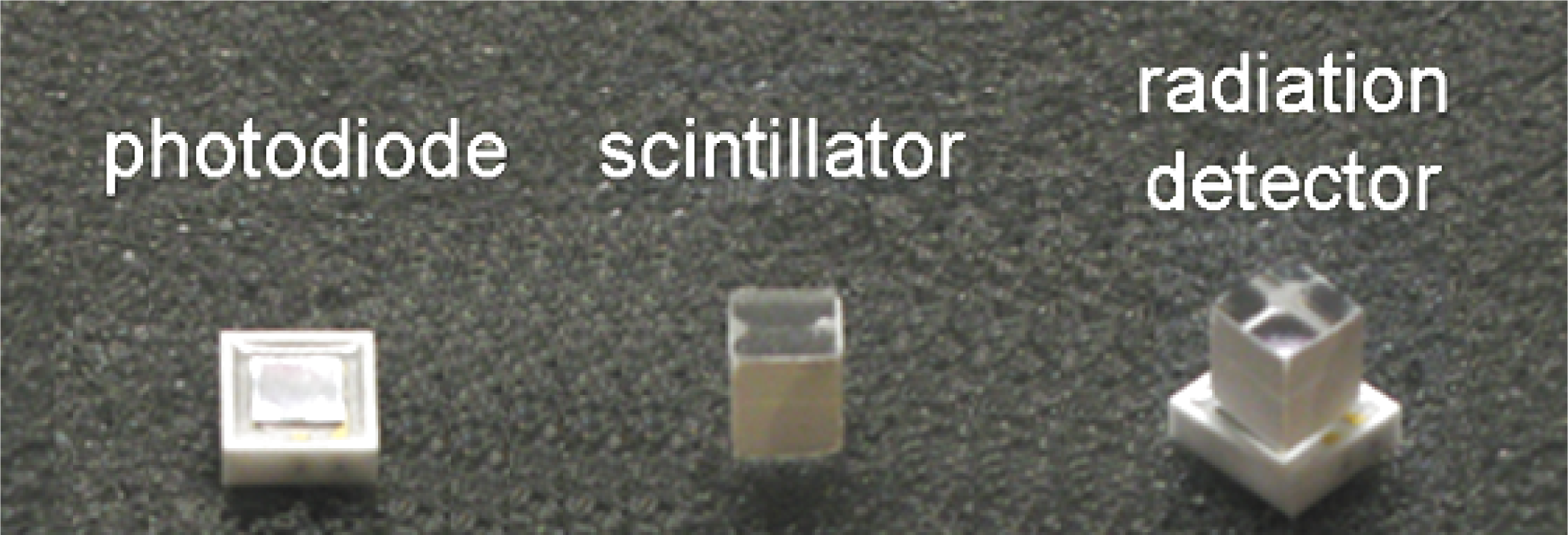
Typically in PET the detection of incident radiation is achieved by a two-step conversion of the annihilation photon energy (1) to visible light in a scintillation material and (2) to electric charge in a photo-detector. Even though inevitable signal losses are associated with this two-step conversion, this type of detector is still considered to be a well understood, fast and efficient means of 511 keV photon detection. An example of a two-step radiation detector is shown in Figure 5.
2.1. The ideal ToF-PET detector
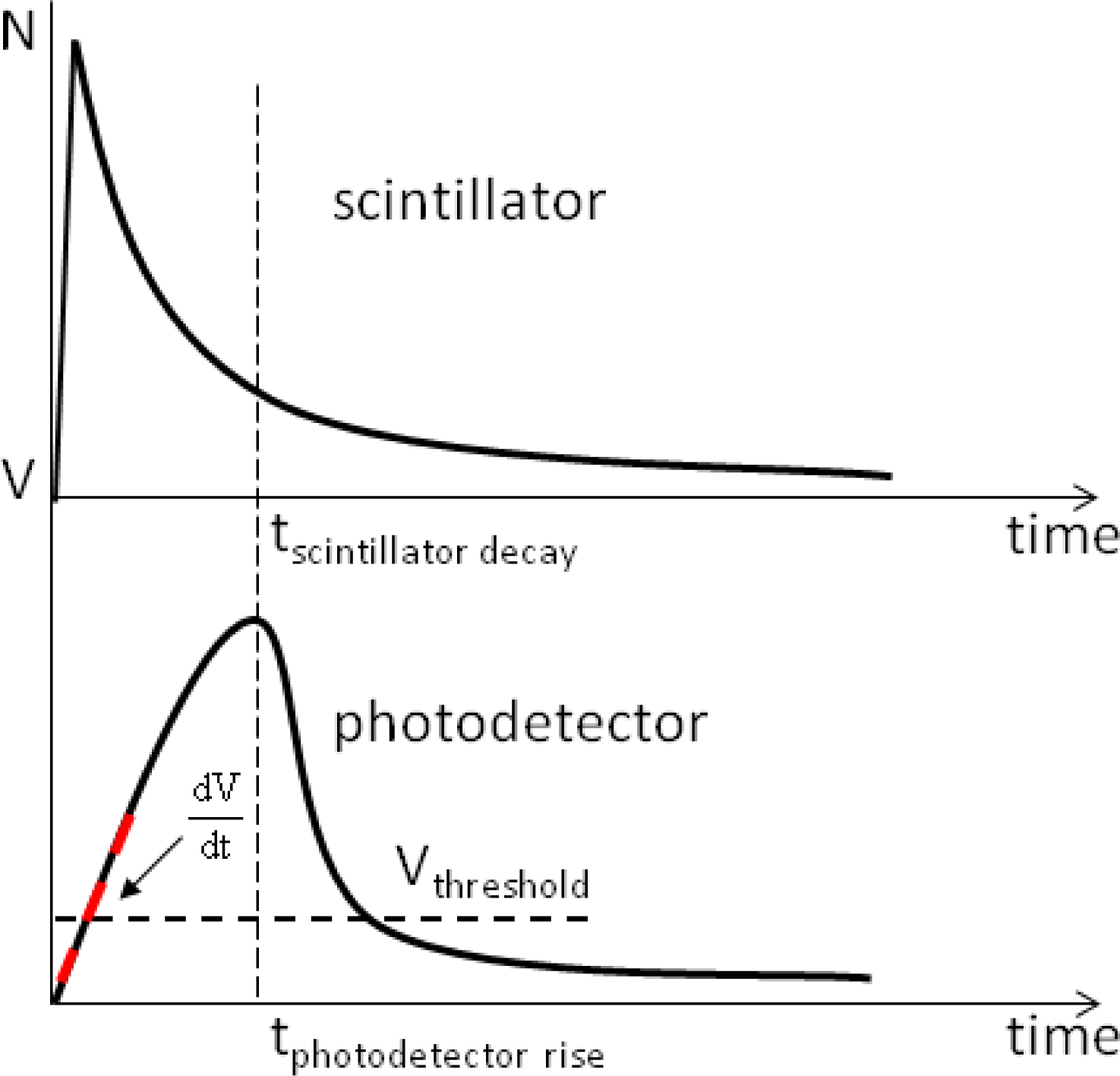
In order to extract as accurately as possible information about the flight time difference of the two annihilation photons, both components of the PET detector, namely the scintillator and the photo-detector, should have a fast, ideally instantaneous response. However, there are a number of factors which may considerably affect time resolution, such as the statistical nature of radiation detection, even in the case of very fast response. Both the detection of the annihilation photons in a scintillation crystal as well as the detection of optical photons in the photo-detector are subject to Poisson statistics which may affect the timing accuracy especially in case of a low scintillation light yield and/or a low photo-detector gain. Thus high light output in the scintillator and high gain in the photo-detector are key features in order to minimize statistical uncertainties.
An ideal ToF-PET radiation detector will combine the following features:
a scintillator material with high efficiency for absorption of the 511-keV annihilation photons
a scintillation process with instantaneous rise and decay times of the light pulse profile
a scintillator geometry with a low aspect ratio ( ) which will minimize the optical photon travel path and thus light losses at the crystal interfaces, as well as transit time variances in the crystal
a photo-detector with high efficiency in the detection of the visible light produced by the scintillator
a photo-detector with high amplification gain and low noise
a photo-detector with instantaneous rise and decay time of the charge pulse profile and low charge transit time spread
2.2. Scintillation crystals
Table 1 summarizes the basic features of fast scintillators that have been considered in ToF-PET, either in research or in industry. As already mentioned in the description of an ideal radiation detector, a scintillator with high photon emission rate (high photon yield at a fast decay time) and high stopping power (as represented by the effective atomic number and the density) is the desired combination for ToF-PET. However additional features such as the refractive index and the peak emission wavelength will assure compatibility with the photo-detector and thus efficient transfer of the optical photon flux from the scintillator to the photo-detector. Even though LSO or LYSO is acknowledged as the option of choice for fast scintillation counters, an even faster and more luminous scintillation material, LaBr3 has recently attracted interest with promising results [19–21] despite its hygroscopic properties and lower stopping power compared to LSO. Recently, the doping of the latter (LSO) with Ca in addition to Ce dopants proves to improve the timing performance of the scintillator.
From the materials listed in Table 1, BaF2 and plastic scintillators are not preferred options for ToF-PET despite their excellent time response. Plastic scintillators suffer from low stopping power and optical photon yield, factors that will significant compromise PET overall imaging performance. The inorganic material BaF2 has been studied in the past as a candidate for ToF [22] with promising results in terms of time resolution reaching values below 300 ps [23]. However, the stopping power and light output of this material is significantly lower compared to the other inorganic scintillators of Table 1 and, in addition, the peak emission wavelength of the fast decay component of BaF2 may restrict the available choices of photo-detectors with sufficient light detection efficiency at this part of the electromagnetic spectrum.
2.3. Photo-detectors
Even with an ideal scintillator yielding high optical photon rate, a lower bound on the time resolution that can be achieved is imposed by the photo-detector performance. Low quantum efficiency (ratio of number of emitted charge to the number of incident optical photons absorbed in the photosensitive area, QE) of the photo-detector at the peak emission wavelength of the scintillator will result in an effective reduction of the amount of scintillation light detected. In addition low gain, gain variations or noise in the photo-detector response will increase statistical variations in the extraction of any type of information from the generated electrical signal. Table 2 summarizes the basic performance features of the three types of photo-detectors widely used in commercial and research PET systems [24,25].
From the photo-detectors listed in Table 2, proportional mode avalanche photo-diodes (APDs) are not preferred for use in the ToF application due to their significantly slower response time. In addition, their low multiplication gain results in small output signals requiring further amplification prior to processing. In the following, two types of photo-detectors will be reviewed, the PMT and the SiPM, with special focus on the latter.
The photomultiplier tube (PMT)
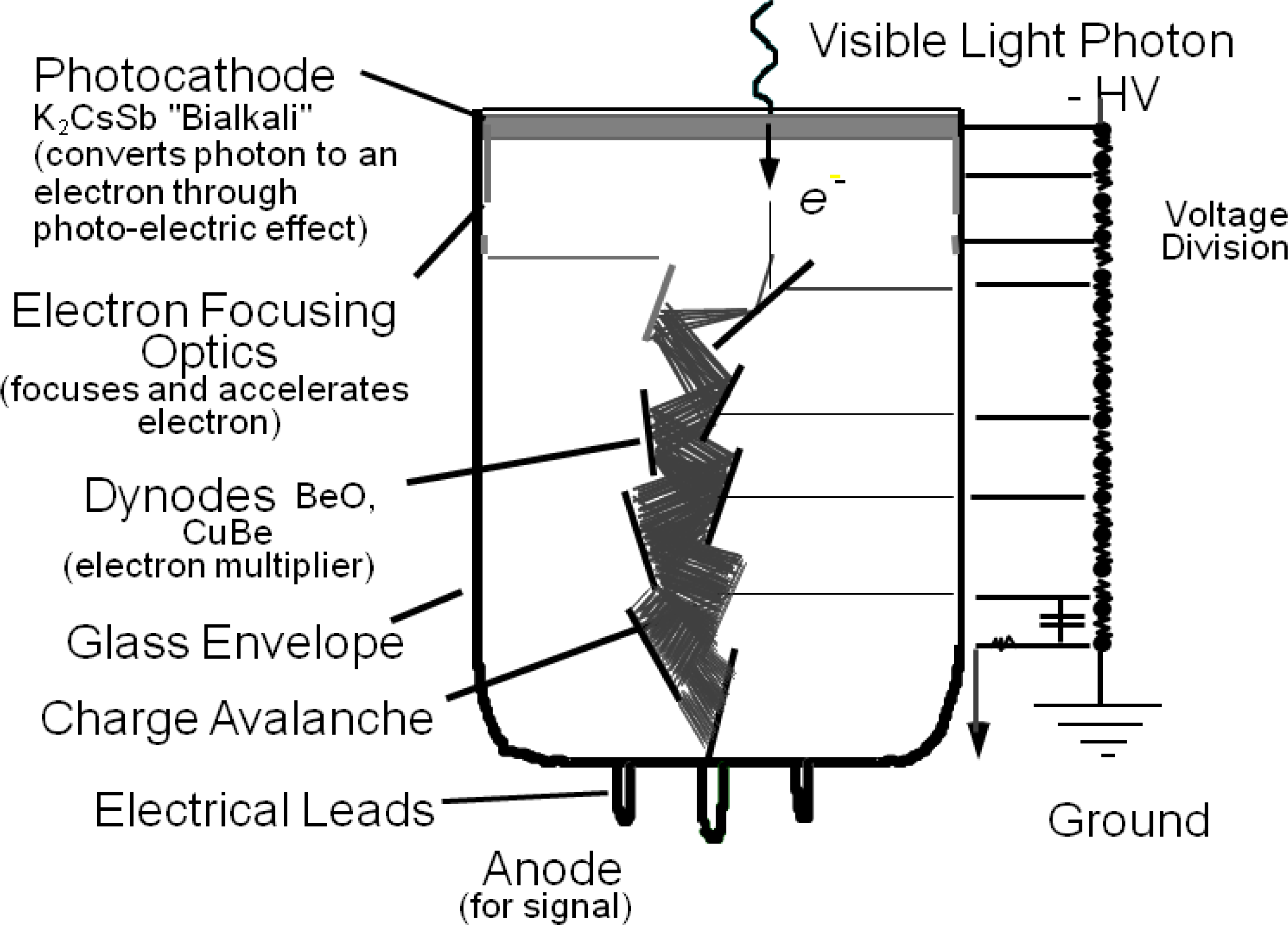
The photomultiplier tube (PMT) is a photo-detector type commonly used for scintillator readout in numerous applications including medical imaging. In ToF-PET, PMTs are still considered to be the gold standard for sub-nanosecond time resolution [12,26]. Their high gain combined with a low excess noise factor lead to minimal deviation from Poisson statistics as well as reduced statistical uncertainty in the generated charge signal [9]. The basic component of a PMT is a vacuum tube consisting of a photo-cathode, several electrodes called dynodes and an anode. The photocathode is a photo-sensitive electrode that emits charge (electrons) for a number of incident optical photons absorbed with a given efficiency (QE defined above). Between the cathode and the anode a bias voltage in the kV range is applied to facilitate the generated electron transport and amplification from the cathode to the anode. Under the influence of a high potential the generated electrons from the photocathode drift and successively encounter the dynode stages. At every dynode stage the incident electrons have gained sufficient energy to create secondary electron emissions from collisions with the dynode, thus resulting in a large electron cloud at the anode (Figure 7). As can be seen in Table 2, one advantage of PMTs over semiconductor photo-detectors is their lower sensitivity in temperature variations which in most cases implies stable detector operation over a wide range of temperatures. However, their relatively bulky size and the requirement for power supplies which can provide thousands of Volts make PMTs a less attractive option for their use in high packing fraction, high channel density PET radiation detectors.
The Silicon photomultiplier (SiPM)
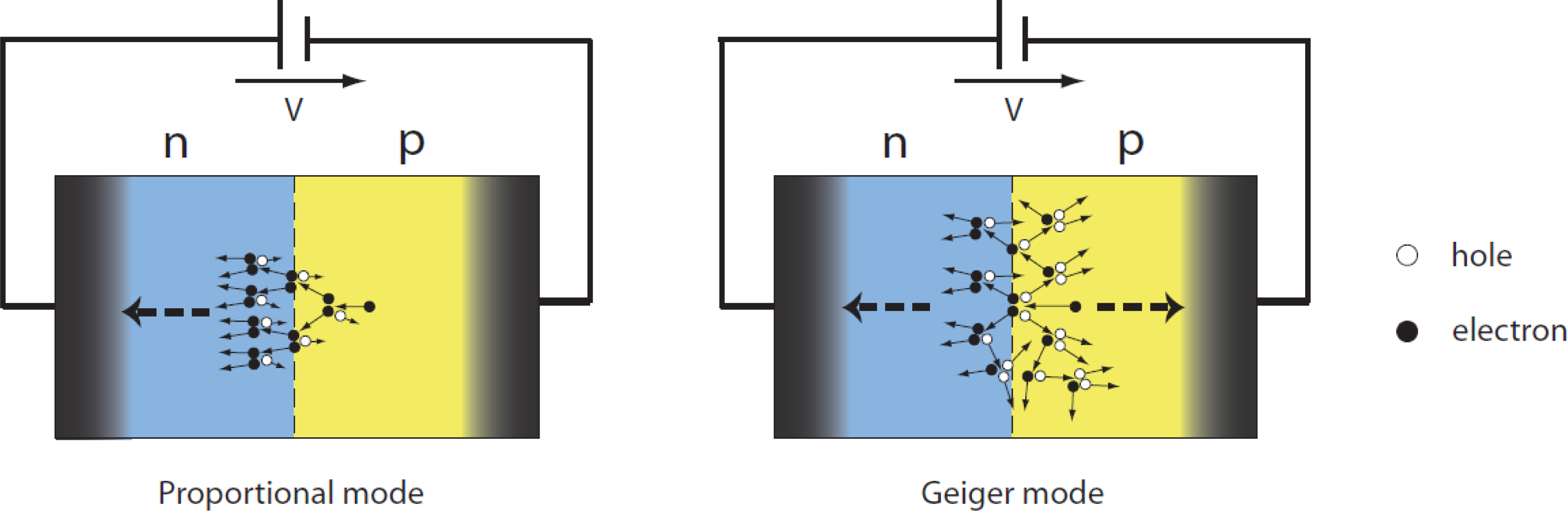
The silicon photomultiplier (SiPM) has recently been introduced to address the shortcomings of both PMTs and APDs summarized in Table 2 [25,27–32]. These devices consist of an array of microscopic, parallel connected avalanche photo-diodes which operate in limited Geiger-mode (alternatively known as G-APDs or SiPM micro-cells). In this mode of operation the micro-cells are biased above breakdown resulting in a cumulative avalanche breakdown within the diode depletion region and thus in an excessive current every time they encounter a (visible) photon stimulus (Figure 8). The difference between the proportional and the Geiger mode of APD operation is illustrated in Figure 9. As shown in Figure 9 in the case of a proportional-mode APD the electron carriers are primarily involved in the avalanche process, while in the case of a Geiger-mode APD both charge carriers (namely electrons and holes) are able to trigger an avalanche.
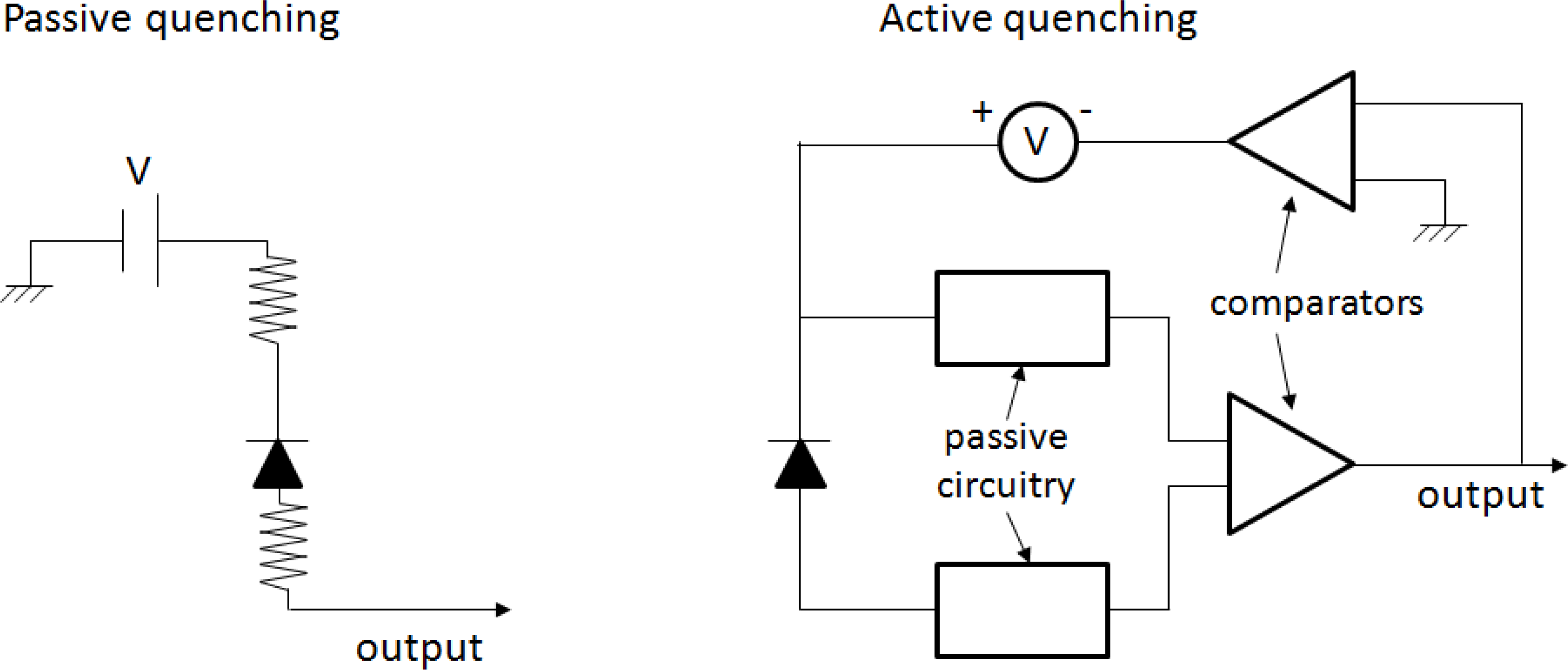
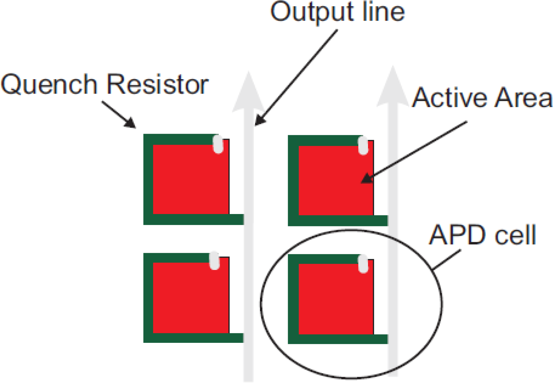
In order for the large amount of current not to destroy the diode, an appropriate quenching circuit is integrated to each micro-cell as shown in Figure 10. Typically, a resistor of several hundreds of kOhm (quenching resistor) is connected in series with each micro-cell to quench the avalanche (passive quenching). Every time a large current flows trough it, it will result in a voltage drop across the micro-cell terminals. This voltage drop is large enough to lower the micro-cell applied bias below the breakdown limit, resulting in interruption of the avalanche process. Due to the inherent micro-cell capacitance, as well as the parasitic capacitance of the overall summing network in a SiPM, each micro-cell needs a characteristic amount of time to recover after the bias voltage is restored to values above breakdown. This characteristic time is called recovery time and its magnitude is typically equal to the product of the value of the quenching resistor and the value of the overall diode capacitance.
Even though passive quenching is relatively simple to implement and most of commercially available SiPMs employ such circuits, there are specific performance limitations associated with it. The pulse shape depends on the values of the passive elements used in the quenching circuitry and may thus be subject to variations depending on how these values are influenced i.e., by temperature. In addition SiPMs with passive quenching are typically characterized by long recovery times which can subsequently impact their count rate performance and dynamic range [34].
In order to address the above shortcomings of passive quenching, G-APDs can alternatively be quenched using an active quenching circuit (Figure 11).
A generic active circuit typically consists of a comparator-based feedback circuit with a sensing and a quenching network. Whenever the rise of the G-APD output pulse is sensed, indicating the rise of an avalanche, a feedback pulse is produced and forces the G-APD to quench the avalanche by means of a controlled voltage source. This source is also configured to reset the G-APD back to an active state by restoring the proper bias across its terminals. Both the quenching and the reset are performed in a highly controlled way allowing thus for fast recovery of the SiPM micro-cells [35]. For applications where high count rate capability is a prerequisite, SiPMs with active quenching are preferred.
Even though the most acknowledged advantage of actively quenched SiPMs is their enhanced count rate performance, they may also demonstrate an effective enhancement in PDE owing to the fact that each micro-cell can be triggered multiple times, within the duration of the light stimulus, due to their fast recovery (factor RT becomes larger in Equation 4). On the other hand, it is difficult to predict quantitatively the actual PDE enhancement because of the limitations in the SiPM fill factor due to the active quenching circuitry (factor FF becomes smaller in Equation 4).
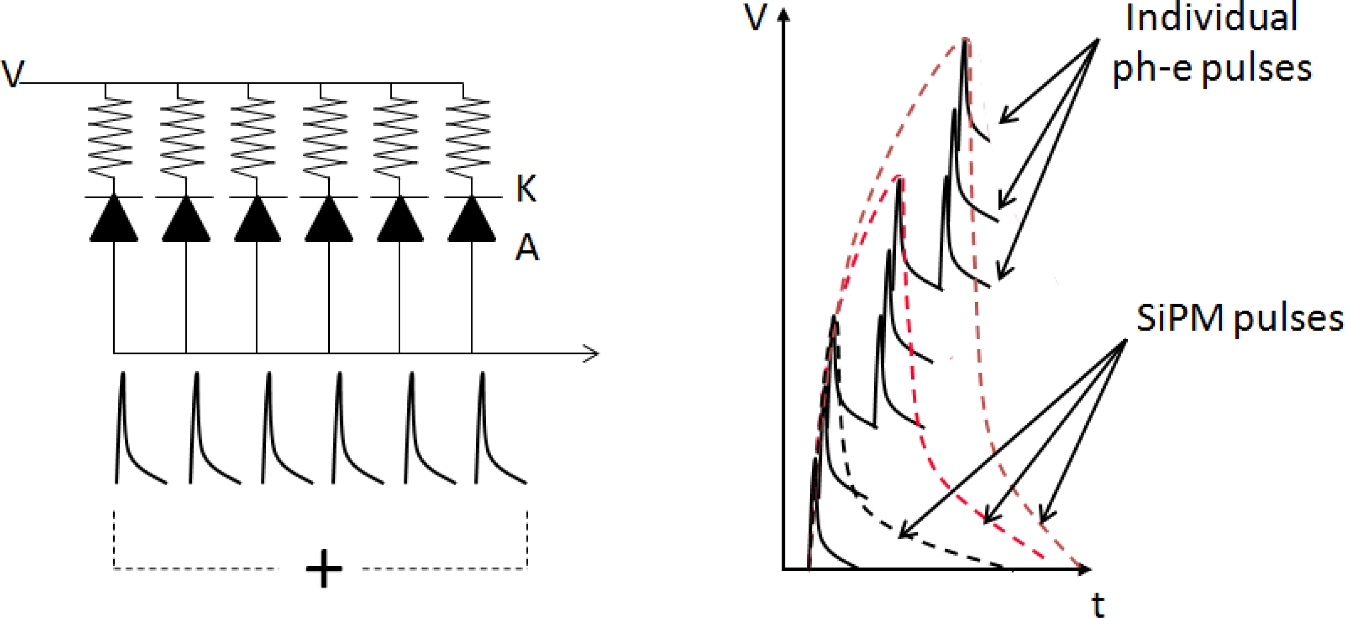
In both the aforementioned quenching modes, every micro-cell acts as a binary device which can provide information about the detection of a light stimulus but no information about its intensity. Proportionality between the intensity of the incident light stimulus and the output charge of a SiPM is achieved by summing the signals of individual micro-cells through a common readout line, provided that the incident photon flux is low enough in order for each micro-cell to respond to a single visible photon (Figures 10 and 12). The SiPM combines appealing detector features of both the PMT and the APD for ToF-PET imaging:
Small size which enables detectors with high packing fraction for enhanced sampling and photon sensitivity. In addition small sensitive area reduces device capacitance and dark current.
High gain which eliminates the need for pre-amplification.
Single electron pulses from each micro-cell with a very well defined pulse shape which can be exploited for optimum timing.
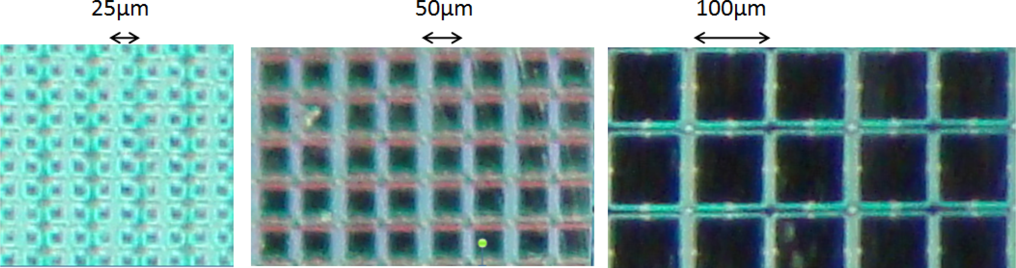
Furthermore in a given SiPM area with a fixed dead area (area occupied by the read-out traces) around each micro-cell, a larger number of micro-cells would imply a smaller micro-cell sensitive area. This decreased micro-cell area decreases the light PDE of each cell and thus, the overall detection efficiency of the device is degraded (Figure 13).
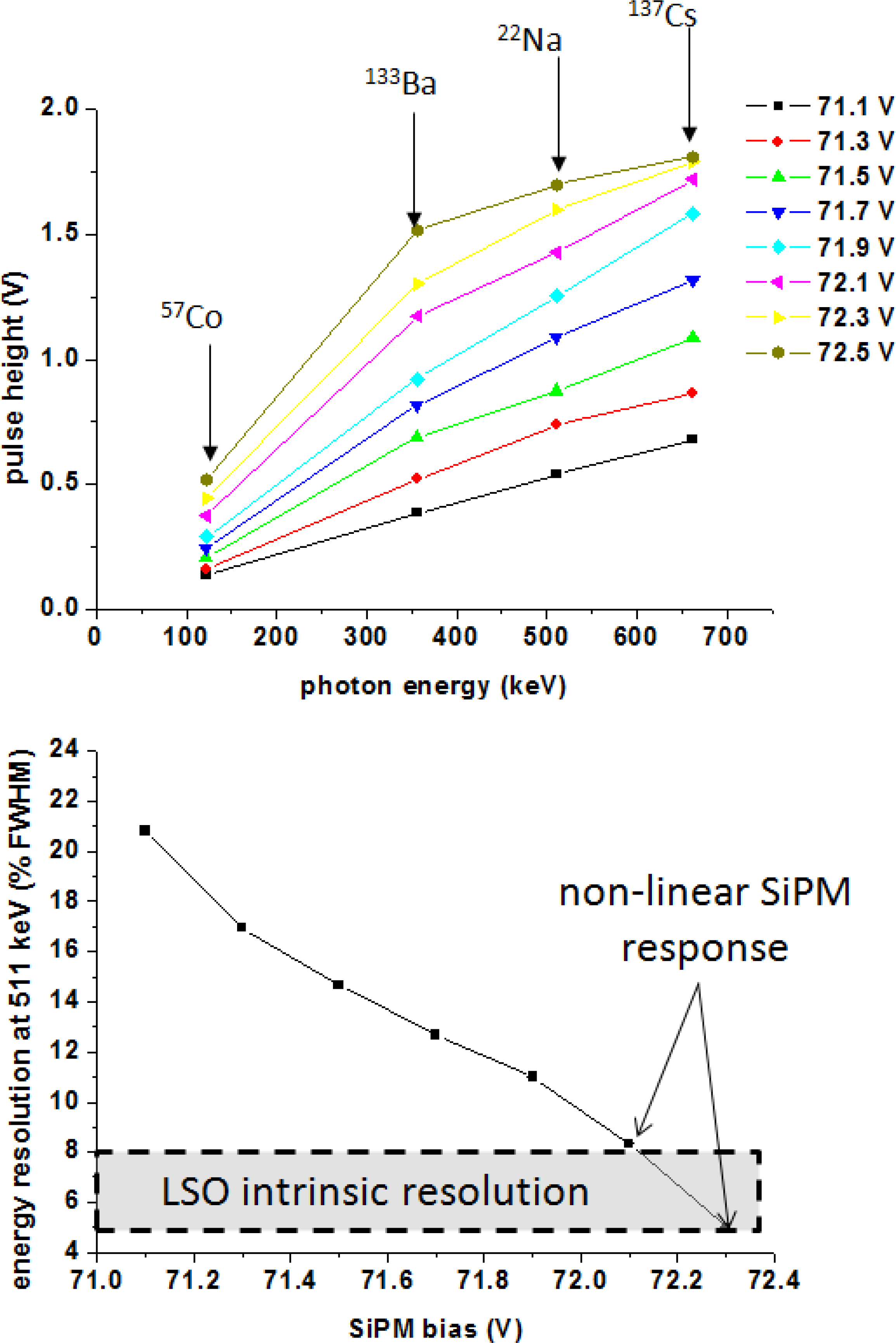
The plots of Figure 14 indicate severe non-linear effects and effects on the energy resolving power of scintillation readout from SiPMs as a function of their applied bias voltage. Above a given value of the applied voltage the measured SiPM response to radiation quanta of different energies is no longer linear (Figure 14, top). An increasing bias voltage leads to increased SiPM gain and PDE, initially resulting in energy resolution improvements. For excessive bias increase, the PDE is high enough to effectively lower the SiPM dynamic range (because the number of optical photons which can trigger an avalanche is no longer related linearly to the number of available micro-cells). In this case, the measured energy resolution values appear to be overestimated, namely below the theoretical limits imposed by the intrinsic resolution of the scintillator (Figure 14, bottom).
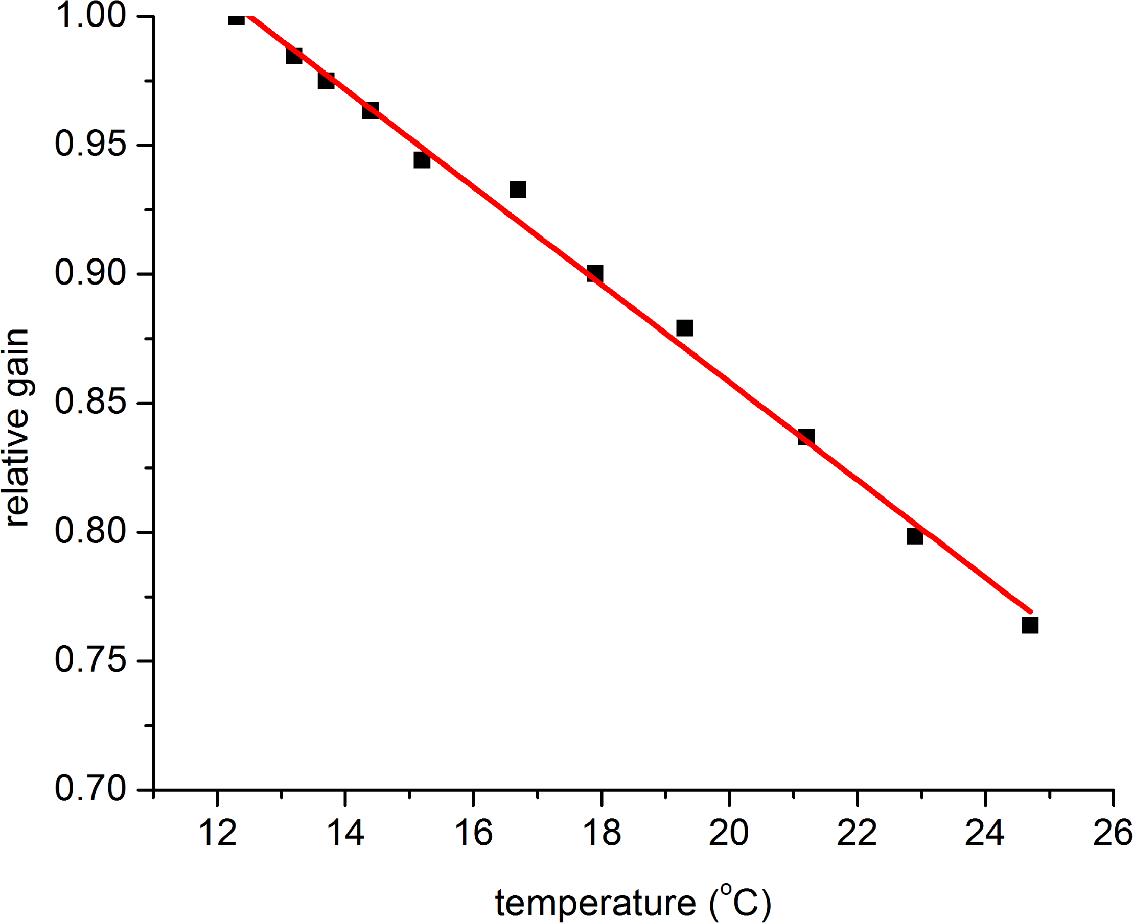
As in any semiconductor, temperature sensitivity of SiPMs is still a major issue affecting the detector’s performance [36,37]. Temperature coefficients varying from 2 to have been measured. As shown in Figure 15, the detector gain is decreased with increasing temperature owing to quenching of a larger part of the avalanche carriers’ energy due to collisions with the crystal lattice vibrations (phonons). In addition, for the majority of SiPMs employing passive quenching, the value of the quenching resistor demonstrates a temperature dependence that may lead to variations in the SiPM pulse shape with further implications on recovery time and timing performance of the devices [38].
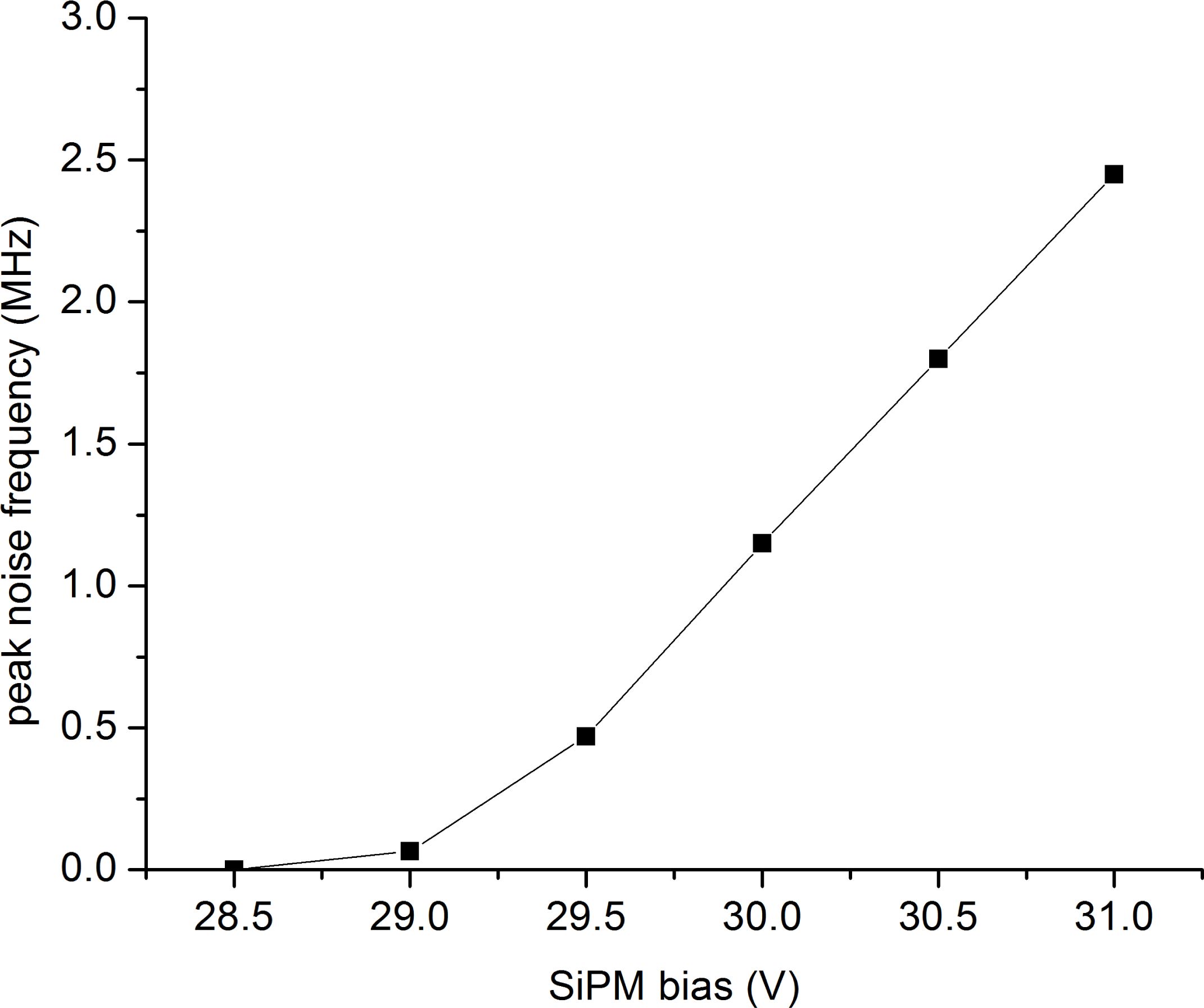
SiPMs are characterized by high dark count rates in the kHz to MHz range. Dark counts are signals induced in the individual micro-cells by a thermal stimulus instead of a light signal. Thermal stimulation is frequent in SiPM micro-cells and can result in an increased signal noise level thus affecting the timing performance of the devices (Equation 2). Figure 16 shows the dependence of the maximum registered dark count frequency on SiPM applied bias. At a given applied bias, multiple dark count rates may exist depending on the triggering threshold at which these rates are measured. This effect is attributed to the optical crosstalk (described below) apparent between different micro-cells of a SiPM, resulting in simultaneous signal generation from multiple micro-cells. The triggering threshold for the measurements shown in Figure 16 is adjusted depending on the applied bias, so that the maximum dark count rate typically from a single micro-cell (denoted as ’peak noise frequency’ in the y-axis of Figure 16) is registered.
An effective increase in the observed SiPM dark count rate is also attributed to after-pulse effects. After-pulses are belated micro-cell excitations following the initial micro-cell excitation due to late release of avalanche charge carriers trapped in defects within the diode sensitive area (depletion region). This phenomenon effectively results in small signals piled up in the tail of the actual SiPM output [39].
The Geiger discharge followed by the excessive avalanche process results in inherent light emission from the micro-cells themselves [40]. The SiPM architecture is such that crosstalk due to distribution of this light between adjacent micro-cells may occur. This process is known as optical crosstalk and leads to falsely stimulated micro-cells and furthermore to an effective decrease of the actual SiPM dynamic range. Optical crosstalk may be further facilitated by optical media such as the SiPM entrance window (typically coated by epoxy or resin) or the scintillation crystal itself.
The aforementioned limitations in SiPM performance are being addressed by a number of specialized designs:
Back-illuminated SiPMs for enhanced PDE [41]
SiPMs with an enhanced p-on-n structure for sensitivity in blue light [42]
SiPMs with quenching resistors in the bulk for elimination of the polysilicon resistor [43]
SiPMs with dual p-n structure for cross-talk elimination [44]
SiPMs with intra-cell trenches for cross-talk elimination [44]
It is expected that in the near future these shortcomings will be eliminated to a large extent. However, despite the aforementioned challenges and limitations, scintillator readout by SiPMs shows great promise for fast timing applications, such as ToF-PET (Figure 17):
3. ToF-PET State of the Art Systems
A number of ToF-PET scanners are currently commercially available. Even though the current generation of ToF-PET systems is based on PMTs, it is expected that in future systems the PET detectors will be SiPM-based in order to utilize compact detector designs while achieving comparable or, potentially, superior time resolution.
Philips TF PET/CT. The basic detector component of the system consists of arrays of LYSO pixels (4 × 4 × 22 mm3 pixel size) read out by hexagonal arrays of PMTs. The achieved time resolution of the system varies between 600 and 900 ps depending on the photon event count rate [46].
Siemens Biograph TruePoint PET/CT. The detectors of this system are arrays of LSO crystal pixels (4×4×20 mm3 pixel size) read out by arrays of PMTs and can achieve 500 ps time resolution [47].
GE Discovery 690. This ToF system also employs arrays of LYSO crystal pixels (pixel size is 4.25 × 6.3 × 25 mm3) read out by PMTs. The achieved time resolution is 600 ps [48].
4. Future of ToF-PET Photo-Detector Technology
4.1. Digital SiPMs
A novel technological advance in the field of semiconductor photo-detectors has been recently developed by Philips and involves the integration within the SiPM sensitive area of basic processing electronics thus eliminating the need for external processing electronics [49,50]. Each micro-cell of the array is connected to an integrated counter (for extraction of energy information) and an integrated time to digital converter (TDC, for extraction of time information). This alternative SiPM design is known as ’digital SiPM’ and time resolutions as low as 150 ps (FWHM) with LYSO readout have been reported.
The development of fully digital photon detection technologies based on single photon avalanche photo-diodes has been reported by other groups [51] even though these technologies have not been tested for annihilation radiation detection. The so-called single-photon synchronous detectors (SPSDs) are able to measure both intensity and phase of the incident light which can be exploited to compute the position of a target based on the phase difference of the light incident to the target and the light reflected by the target and detected by the SPSD.
Apart from the obvious advantage of simplified external signal processing characterizing the digital implementation of single photon detectors, there are some potential disadvantages associated with this technology, which include an increase in power consumption, as well as reduced fill factor due to the space required for the additional electronic circuits. In addition, since the analog form of the generated signal is not available, there may be some lack of useful information content, mostly associated with pulse shape variations.
4.2. Discrete amplification photodiodes
Another SiPM design that aims to address both the limited PDE and the recovery time issues of passive quenching is employed by discrete amplification photo-diodes (DAPDs) [52,53]. The internal architecture of these devices is fundamentally different from the micro-cell array concept of traditional SiPMs. The charge produced from a single photosensitive area is distributed to a number of discrete amplifiers which are integrated in the diode’s bulk. Each charge packet will be subject to individual amplification and the output signal will be the sum of the amplified charge packets. Due to the absence of long traces surrounding each micro-cell, DAPDs have very low capacitance which results in short recovery times.
Acknowledgments
The authors would like to thank Farhad Taghibakhsh (Stanford University) for carefully reviewing the manuscript. The help of Jing-Yu Cui (Stanford University) and Nepomuk Otte (University of California Santa Cruz) with a few of the illustrations is greatly acknowledged. This work is supported in part by the AXA research Fund.
References
- Cherry, S; Sorenson, J; Phelps, M. Physics in Nuclear Medicine; Elsevier Health Science: New York, NY, USA, 2003. [Google Scholar]
- Budinger, T. Time-of-flight positron emission tomography-status relative to conventional PET. J. Nucl. Med 1983, 24, 73–76. [Google Scholar]
- Mullani, N; Ficke, D; Hartz, R; Markham, J; Wong, G. System design of fast PET scanners utilizing time-of-flight. IEEE Trans. Nucl. Sci 1981, 28, 104–1077. [Google Scholar]
- Moses, W. Recent Advances and Future Advances in Time-of-Flight PET. Nucl. Instr. Meth. Phys. Res. A 2007, 580, 919–924. [Google Scholar]
- Levin, C; Hoffman, E. Calculation of positron range and its effect on the fundamental limit of positron emission tomography system spatial resolution. Phys. Med. Biol 1999, 44, 781–799. [Google Scholar]
- Karp, J; Surti, S; Daube-Witherspoon, M; Muehllehner, G. Benefit of time-of-flight in PET: Experimental and clinical results. J. Nucl. Med 2008, 49, 462–470. [Google Scholar]
- Surti, S; Karp, J; Popescu, L; Daube-Witherspoon, ME; Werner, M. Investigation of Time-of-Flight Benefit for fully 3D PET. IEEE Trans. Med. Imaging 2006, 25, 529–538. [Google Scholar]
- Surti, S; Karp, J. Experimental evaluation of a simple lesion detection task with time-of-flight. Phys. Med. Biol 2009, 54, 373–384. [Google Scholar]
- Knoll, G. Radiation Detection and Measurement; Wiley: New York, NY, USA, 2001. [Google Scholar]
- Paulus, T. Principles and Applications of Timing Spectroscopy. Application Note AN-42, EG&E 1982. [Google Scholar]
- Bell, R. Comparison of leading-edge and crossover timing in coincidence measurements. Nucl. Instr. Meth. Phys. Res. A 1966, 42, 211–212. [Google Scholar]
- Szczesniak, T; Moszynski, M; Swiderski, L; Nassalski, A; Lavoute, P; Kapusta, M. Fast Photomultipliers for TOF PET. IEEE Trans. Nucl. Sci 2009, 56, 173–181. [Google Scholar]
- Derenzo, S; Weber, M; Moses, W; Dujardin, C. Measurements of the Intrinsic Rise Times of Common Inorganic Scintillators. IEEE Trans. Nucl. Sci 2000, 47, 860–864. [Google Scholar]
- Spurrier, M; Szupryczynski, P; Rothfuss, H; Yang, K; Carey, AA; Melcher, CL. The effect of co-doping in the growth stability and scintillation properties of lutetium oxyorthosilicate. J. Cryst. Growth 2008, 310, 2110–2114. [Google Scholar]
- Szczesniak, T; Moszynski, M; Syntfeld-Kazuch, A; Swiderski, L; Koschan, MAS; Melcher, CL. Timing resolution and decay time of LSO crystals co-doped with calcium. IEEE Trans. Nucl. Sci 2010, 57, 1329–1334. [Google Scholar]
- Syntfeld-Kazuch, A; Moszynski, M; Swiderski, L; Szczesniak, T; Nassalski, A; Melcher, CL; Spurrier, MA; Goliszek, B; Kaminski, P; Nowaczyk, M. Energy Resolution of Calcium Co-doped LSO:Ce Scintillators. IEEE Trans. Nucl. Sci 2009, 56, 2972–2978. [Google Scholar]
- van Loef, E; Dorenbos, P; van Eijk, C; Krämer, K; Güdel, HU. High-energy-resolution scintillator: Ce3+ activated LaBr3. Appl. Phys. Lett 2001, 79, 1573. [Google Scholar]
- Saint Gobain. Available online: http://www.detectors.saint-gobain.com (accessed on 25 October 2010).
- Kuhn, A; Surti, S; Karp, J; Raby, PS; Shah, KS; Perkins, AE; Muehllehner, G. Design of a lanthanum bromide detector for time-of-flight PET. IEEE Trans. Nucl. Sci 2004, 51, 2550–2557. [Google Scholar]
- Schaart, D; Seifert, S; Vinke, R; van Dam, HT; Dendooven, P; Löhner, H; Beekman, FJ. LaBr3:Ce and SiPMs: achieving 100 ps coincidence resolving time. Phys. Med. Biol 2010, 55, N179–N189. [Google Scholar]
- Daube-Witherspoon, M; Surti, S; Perkins, A; Kyba, CCM; Wiener, R; Kulp, R; Karp, JS. The imaging performance of a LaBr3-based PET scanner. Phys. Med. Biol 2010, 55, 45–64. [Google Scholar]
- Laval, M; Moszynski, M; Allemand, R; Cormoreche, E; Guinet, P; Ordu, R; Vacher, J. Barium Fluoride - Inorganic scintillator for subnanosecond timing. Nucl. Instr. Meth. Phys. Res. A 1983, 206, 169–176. [Google Scholar]
- Ziegler, S; Ostertag, H; Kuebler, W; Lorenz, WJ; Otten, EW. Effects of scintillation collection on the time resolution of a time-of-flight detector for annihilation quanta. IEEE Trans. Nucl. Sci 1990, 37, 574–579. [Google Scholar]
- Wernick, M; Aarsvold, J. Emission Tomography: The fundamentals of PET and SPECT; Elsevier Academic Press: San Diego, CA, USA, 2004; pp. 53–88. [Google Scholar]
- Renker, D. Geiger-mode avalanche photodiodes, history, properties and problems. Nucl. Instr. Meth. Phys. Res. A 2006, 567, 48–56. [Google Scholar]
- Moszynski, M; Kapusta, M; Nassalski, A; Szczesniak, T; Wolski, D; Eriksson, L; Melcher, CL. New Prospects for Time-of-Flight PET With LSO Scintillators. IEEE Trans. Nucl. Sci 2006, 53, 2484–2488. [Google Scholar]
- Renker, D. New trends on photodetectors. Nucl. Instr. Meth. Phys. Res. A 2007, 571, 1–6. [Google Scholar]
- Nassalski, A; Moszynski, M; Syntfeld-Kazuch, A; Szczesniak, T; Swiderski, L; Wolski, D; Batsch, T; Baszak, J. Multi Pixel Photon Counters (MPPC) as an Alternative to APD in PET Applications. IEEE Trans. Nucl. Sci 2010, 57, 1008–1014. [Google Scholar]
- Kim, C; Wang, GC; Dolinsky, S. Multi-Pixel Photon Counters for TOF PET Detector and Its Challenges. IEEE Trans. Nucl. Sci 2009, 56, 2580–2585. [Google Scholar]
- Mazillo, M; Condorelli, G; Sanfilippo, D; Valvo, G; Carbone, B; Fallica, G; Billota, S; Belluso, M; Bonanno, G; Cosentino, L; Pappalardo, A; Finocchiaro, P. Silicon Photomultiplier Technology at STMicroelectronics. IEEE Trans. Nucl. Sci 2009, 56, 2434–2442. [Google Scholar]
- Piemonte, C; Battiston, R; Boscardin, M; Dalla Betta, G-F; Del Guerra, A; DInu, N; Pozza, A; Zorzi, N. Characterization of the First Prototypes of Silicon Photomultiplier Fabricated at ITC-irst. IEEE Trans. Nucl. Sci 2007, 54, 236–244. [Google Scholar]
- Stewart, A; Saveliev, V; Bellis, S; Herbert, DJ; Hughes, PJ; Jackson, JC. Performance of 1-mm2 Silicon Photomultiplier. IEEE J. Quantum Electron 2008, 44, 157–164. [Google Scholar]
- Otte, A. Observation of VHE γ-Rays from the Vicinity of Magnetized Neutron Stars and Development of New Photon-Detectors for Future Ground based γ-Ray Detectors. PhD thesis, Technische Universitaet Muenchen, Germany. 2007. [Google Scholar]
- Spanoudaki, V; Mann, A; Otte, A; Konorov, I; Torres-Espallardo, I; McElroy, DP; Ziegler, SI. Use of single photon counting detector arrays in combined PET/MR: Characterization of LYSO-SiPM detector modules and comparison with a LSO-APD detector. J Instrum 2007, P12002. [Google Scholar]
- Cova, S; Ghioni, M; Lacaita, A; Samori, C; Zappa, F. Avalanche photodiodes and quenching circuits for single-photon detection. Applied Opt 1996, 35, 1956–1976. [Google Scholar]
- Sze, S. Physics of semiconductor devices; Wiley Interscience, 1981. [Google Scholar]
- Petasecca, M; Alpat, B; Ambrossi, G; Azzarello, P; Battiston, R; Ionica, M; Papi, A; Pignatel, GU; Haino, S. Thermal and Electrical Characterization of Silicon Photomultiplier. IEEE Trans. Nucl. Sci 2008, 55, 1686–1690. [Google Scholar]
- Tur, C; Solovyev, V; Flamanc, J. Temperature characterization of scintillation detectors using solid-state photomultipliers for radiation monitoring applications. Nucl. Instr. Meth. Phys. Res. A 2010, 620, 351–358. [Google Scholar]
- Du, Y; Retiere, F. After-pulsing and cross-talk in multi-pixel photon counters. Nucl. Instr. Meth. Phys. Res. A 2008, 596, 396–401. [Google Scholar]
- Otte, A. On the efficiency of photon emission during electrical breakdown in silicon. Nucl. Instr. Meth. Phys. Res. A 2009, 610, 105–109. [Google Scholar]
- Ninkovic, J; Hartmann, R; Holl, P; Lutz, G; Merck, C; Mizroyan, R; Hans-Günther, M; Otte, A-N; Richter, R; Soltau, H; Teshima, M. The Avalanche drift diode-A backilluminated Silicon Photomultiplier. Nucl. Instr. Meth. Phys. Res. A 2007, 572, 454–455. [Google Scholar]
- Piemonte, C. A new Silicon Photomultiplier structure for blue light detection. Nucl. Instr. Meth. Phys. Res. A 2006, 568, 224–232. [Google Scholar]
- Ninkovic, J; Andricek, L; Liemann, G; Lutz, G; Hans-Günther, M; Richter, R; Schopper, F. SiMPI– An avalanche diode array with bulk integrated quench resistors for single photon detection. Nucl. Instr. Meth. Phys. Res. A 2010, 617, 407–410. [Google Scholar]
- Buzhan, P; Dolgoshein, B; Ilyin, A; Kaplin, V; Klemin, S; Mizroyan, R; Popova, E; Teshima, M. The cross-talk problem in SiPMs and their use as light sensors for imaging atmospheric Cherenkov telescopes. Nucl. Instr. Meth. Phys. Res. A 2009, 610, 131–134. [Google Scholar]
- Llosa, G; Battiston, R; Belcari, N; Boscardin, M; Collazuol, G; Corsi, F; Dalla Betta, G-F; Del Guerra, A; DInu, N; Levi, G; Marcatili, S; Moehrs, S; Marzocca, C; Piemonte, C; Pozza, A. Novel Silicon Photomultipliers for PET Applications. IEEE Trans. Nucl. Sci 2008, 55, 877–881. [Google Scholar]
- Surti, S; Kuhn, A; Werner, ME; Perkins, AE; Kolthammer, J; Karp, JS. Performance of Philips Gemini TF PET/CT Scanner with Special Consideration for Its Time-of-Flight Imaging Capabilities. J. Nucl. Med 2007, 48, 471–480. [Google Scholar]
- Jakoby, B; Bercier, Y; Conti, M; Casey, M; Gremillion, T; Hayden, C; Bendriem, B; Townsend, DW. Performance Investigation of a Time-of-Flight PET/CT Scanner. Proceedings of Nuclear Science Symposium Conference Record, 2008 NSS’08, Dresden, Germany, October 19–25, 2008; pp. 3738–3743.
- Wilson, J; Turkington, T. TOF-PET Small-Lession Image Quality Measured Over a Range of Phantom Sizes. Proceedings of Nuclear Science Symposium Conference Record (NSS/MIC), Orlando, FL, USA, October 24, 2009–November 1, 2009; pp. 3710–3714.
- Degenhardt, C; Prescher, G; Frach, T; Thon, A; de Gruyter, R; Schmitz, A; Ballizany, R. The Digital Silicon Photomultiplier–A Novel sensor for the Detection of Scintillation Light. Proceedings of Nuclear Science Symposium Conference Record (NSS/MIC), Orlando, FL, USA, October 24, 2009–November 1, 2009; pp. 2383–2386.
- Frach, T; Prescher, G; Degenhardt, C; de Gruyter, R; Schmitz, A; Ballizany, R. The Digital Silicon Photomultiplier–Principle of Operation and Intrinsic Detector Performance. Proceedings of Nuclear Science Symposium Conference Record (NSS/MIC), Orlando, FL, USA, October 24, 2009–November 1, 2009; pp. 1959–1965.
- Niclass, C; Favi, C; Kluter, T; Monnier, F; Charbon, E. Single-photon synchronous detection. IEEE J. Solid-State Circuits 2009, 44, 1977–1989. [Google Scholar]
- Linga, K; Godik, E; Seemungal, W; Shushakov, D; Shubin, VE. Ultra low noise photodetectors with internal discrete amplification. Proc. SPIE 2005, 5726, 43–51. [Google Scholar]
- Linga, K; Godik, E; Krutovl, J; Shushakov, D; Shubin, VE; Vinogradov, SL; Levin, EV. Solid State Photomiltiplier: Noise Parameters of Photodetectors with Internal Discrete Amplification. Proc SPIE 2006, 6119. [Google Scholar]


| LSO(Ce) | LSO(Ce, Ca) | LYSO(Ce) | LaBr3 | BaF2 | Plastic | |
|---|---|---|---|---|---|---|
| Density ( ) | 7.40 | similar to LSO | similar to LSO | 5.29 | 4.89 | 1.03 |
| Effective atomic number (Z) | 66 | similar to LSO | similar to LSO | 46 | 54 | 12 |
| Rise time (ns) | ≤ 0:5 | similar to LSO | similar to LSO | 0.2–0.5 | ∼0.03 | 0.7–1 |
| Decay time (ns) | 40 | [email protected]% Ca | similar to LSO | 15–26 | 0.8/620 | 2–5 |
| Photon yield/keV | 20–30 | ∼35 | similar to LSO | 63 | 1.8/10 | 10 |
| Refractive index (n) | 1.82 | 1.82 | 1.82 | 1.90 | 1.56 | 1.58 |
| Hygroscopic | No | No | No | Yes | Slightly | No |
| Peak emission wavelength (nm) | 420 | 420 | similar to LSO | 380 | 220/310 | Various |
| PMT | APD | SiPM | |
|---|---|---|---|
| Gain | 106 | 50–1,000 | ∼106 |
| rise time (ns) | ∼1 | ∼5 | ∼1 |
| QE @ 420 nm (%) | ∼25 | ∼70 | ∼25–75 (PDE) |
| Bias (V) | >1,000 | 300–1,000 | 30–80 |
| Temperature sensitivity ( ) | <1 | ∼3 | 1–8 |
| Magnetic field sensitivity | yes | no | no |
| Sensitive area | cm2 | mm2 | mm2 |
| Price/channel ($) | >200 | ∼100 | ∼50 |
© 2010 by the authors; licensee MDPI, Basel, Switzerland. This article is an open access article distributed under the terms and conditions of the Creative Commons Attribution license (http://creativecommons.org/licenses/by/3.0/.)
Share and Cite
Spanoudaki, V.C.; Levin, C.S. Photo-Detectors for Time of Flight Positron Emission Tomography (ToF-PET). Sensors 2010, 10, 10484-10505. https://doi.org/10.3390/s101110484
Spanoudaki VC, Levin CS. Photo-Detectors for Time of Flight Positron Emission Tomography (ToF-PET). Sensors. 2010; 10(11):10484-10505. https://doi.org/10.3390/s101110484
Chicago/Turabian StyleSpanoudaki, Virginia Ch., and Craig S. Levin. 2010. "Photo-Detectors for Time of Flight Positron Emission Tomography (ToF-PET)" Sensors 10, no. 11: 10484-10505. https://doi.org/10.3390/s101110484