Characterization of a Photodiode Coupled with a Si Nanowire-FET on a Plastic Substrate

Abstract
:
1. Introduction
2. Experimental Procedure
3. Results and Discussion
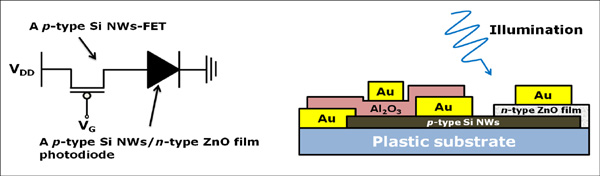
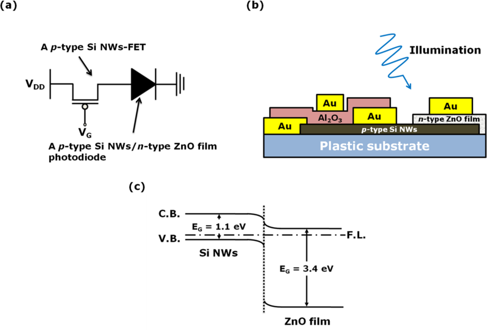
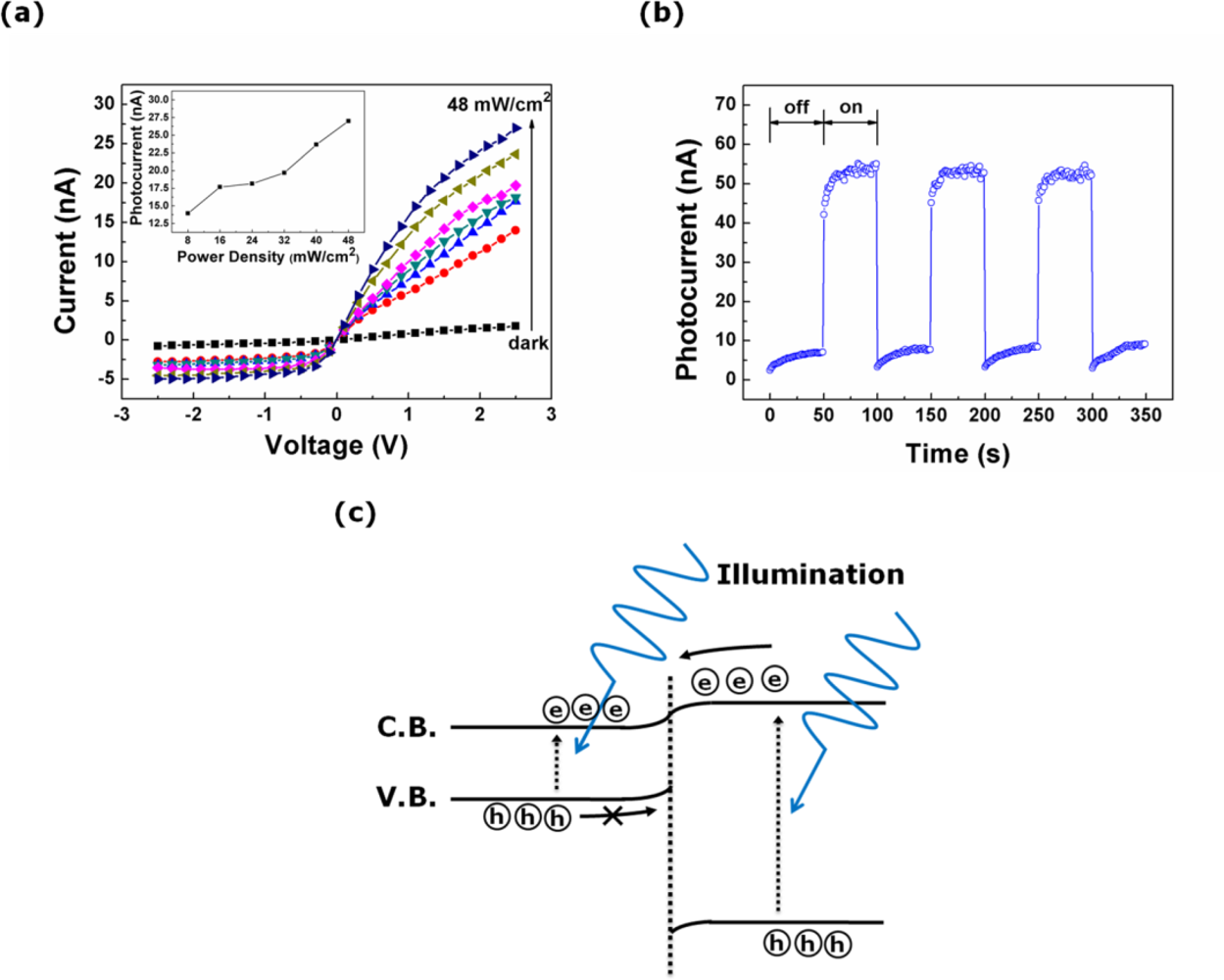
3.1. The Optoelectronic Characteristics of the Single Photodiode Composed of the Transferred p-type Si NWs and the n-type ZnO Film
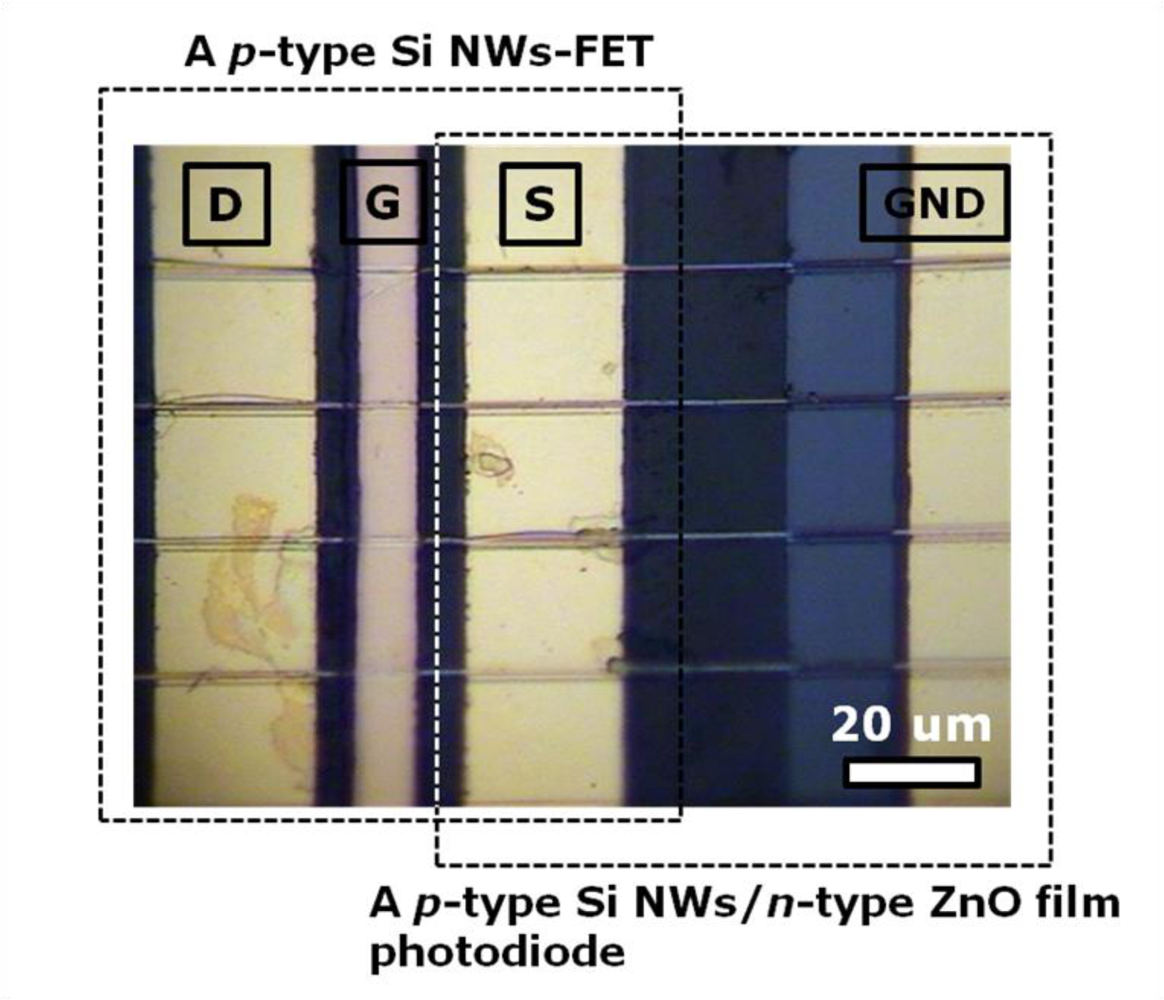
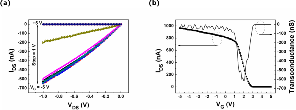
3.2. The Electrical Characteristics of the Transferred p-type Si NWs-FET
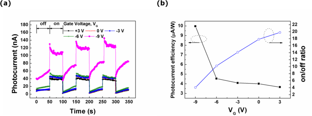
3.3. Characteristics of the Photodiode Modulated by the Operation of the FET in the Laterally Coupled Device
4. Conclusions
Supplemental Information
sensors-10-09118-s001.pdfAcknowledgments
References
- Jang, J; Cho, K; Byun, K; Hong, WS; Kim, S. Optoelectronic Characteristics of HgSe Nanoparticle Film Spin-Coated on Flexible Plastic Substrates. Jpn J Appl Phys 2010, 49, 030210:1–030210:3. [Google Scholar]
- Byun, K; Cho, K; Kim, S. Sintering Effect on the Optoelectronic Characteristics of HgSe Nanoparticle Film on Plastic Substrates. Mater. Chem. Phys 2010, 122, 246–249. [Google Scholar]
- Huang, J; Li, G; Yang, Y. A Semi-Transparent Plastic Solar Cell Fabricated by a Lamination Process. Adv. Mater 2008, 20, 415–419. [Google Scholar]
- Lau, SP; Yang, H; Yu, SF; Yeun, C; Leong, ESP; Li, H; Hng, HH. Flexible Ultraviolet Random Lasers Based on Nanoparticles. Small 2005, 1, 956–959. [Google Scholar]
- Sun, Y; Kim, HS; Menard, E; Kim, S; Adesida, I; John, AR. Printed Arrays of Aligend GaAs Wires for Flexible Transistors, Diode, and Circuits on Plastic Substrates. Small 2006, 11, 1330–1334. [Google Scholar]
- Michael, CM; Habib, A; Dunwei, W; James, RH. Highly Ordered Nanowire Arrays on Plastic Substrates for Ultrasensitive Flexible Chemical Sensors. Nat. Mater 2007, 6, 379–384. [Google Scholar]
- Sun, Y; John, AR. Fabricating Semiconductor Nano/Microwires and Transfer Printing Ordered Arrays of Them onto Plastic Substrates. Nano Lett 2004, 4, 1953–1959. [Google Scholar]
- Lee, KN; Jung, SW; Kim, WH; Lee, MH; Shin, KS; Seong, WK. Well Controlled Assembly of Silicon Nanowires by Nanowire Transfer Methode. Nanotechnol 2007, 18, 445302:1–445302:7. [Google Scholar]
- Chung, EA; Koo, J; Lee, M; Jeong, DY; Kim, S. Enhancement-Mode Silicon Nanowire Field-Effect Transistors on Plastic Substrates. Small 2009, 5, 1821–1835. [Google Scholar]
- Lee, M; Koo, J; Chung, EA; Jeong, DY; Koo, YS; Kim, S. Silicon Nanowire-Based Tunneling Field-Effect Transistors on Flexible Plastic Substrates. Nanotechnol 2009, 20, 455201. [Google Scholar]
- Bae, HS; Im, S. Ultraviolet Detecting Properties of ZnO-Based Thin Film Transtors. Thin Solid Films 2004, 469–470, 75–79. [Google Scholar]
- Bae, HS; Yoon, MH; Kim, JH; Im, S. Photodetecting Properties of ZnO-Based Thin-Film Transistors. Appl. Phys. Lett 2003, 83, 5313–5315. [Google Scholar]
- Koo, J; Kim, S. Charge Transport Modulation of Silicon Nanowire by O2 Plasma. Solid State Sci 2009, 11, 1870–1874. [Google Scholar]
- Masuda, S; Kitamura, K; Okunura, Y; Miyatake, S; Tabata, H; Kawai, T. Transparent Thin Film Transistors Using ZnO as an Active Channel Layer and Their Electrical Properties. J. Appl. Phys 2003, 93, 1624–1630. [Google Scholar]
- Mridha, S; Basak, D. Ultraviolet and Visible Photoresponse Properties of n-ZnO/p-Si Heterojunction. J Appl Phys 2007, 101, 083102:1–083102:5. [Google Scholar]
- Ghosh, R; Basak, D. Electrical and Ultraviolet Photoresponse Properties of Quasialigned ZnO Nanowires/p-Si Heterojunction. App Phys Lett 2007, 90, 243106:1–243106:3. [Google Scholar]


© 2010 by the authors; licensee MDPI, Basel, Switzerland. This article is an open access article distributed under the terms and conditions of the Creative Commons Attribution license (http://creativecommons.org/licenses/by/3.0/).
Share and Cite
Kwak, K.; Cho, K.; Kim, S. Characterization of a Photodiode Coupled with a Si Nanowire-FET on a Plastic Substrate. Sensors 2010, 10, 9118-9126. https://doi.org/10.3390/s101009118
Kwak K, Cho K, Kim S. Characterization of a Photodiode Coupled with a Si Nanowire-FET on a Plastic Substrate. Sensors. 2010; 10(10):9118-9126. https://doi.org/10.3390/s101009118
Chicago/Turabian StyleKwak, Kiyeol, Kyoungah Cho, and Sangsig Kim. 2010. "Characterization of a Photodiode Coupled with a Si Nanowire-FET on a Plastic Substrate" Sensors 10, no. 10: 9118-9126. https://doi.org/10.3390/s101009118