
Carrier Modulation Layer-Enhanced Organic Light-Emitting Diodes


Abstract
:
1. Introduction


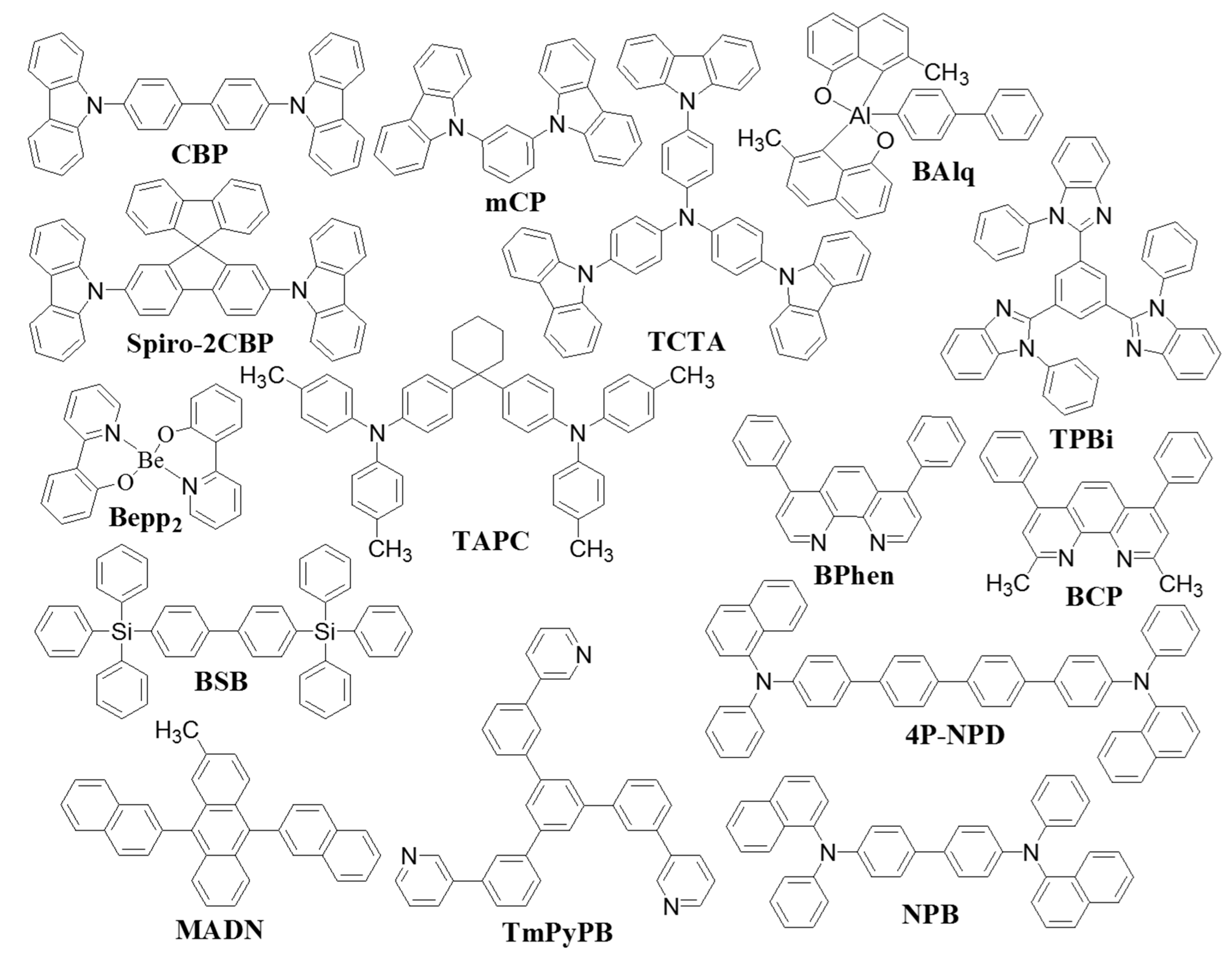
| Material | ET (eV) | Eg (eV) | HOMO (eV) | LUMO (eV) | μh cm2·V−1·s−1 | μe cm2·V−1·s−1 | Reference |
|---|---|---|---|---|---|---|---|
| CBP | 2.6 | 3.5 | −6.0 | −2.9 | 2 × 10⁻³ | 3.0 × 10⁻⁴ | [57,58] |
| Spiro-2CBP | -- | 3.38 | −5.03 | −1.65 | 1 × 10⁻³ | - | [58,59] |
| mCP | 2.9 | 3.5 | −6.1 | −2.4 | 5 × 10⁻⁴ | - | [60] |
| TCTA | 2.79 | 3.4 | −5.7 | −2.3 | 3 × 10⁻³ | 1.0 × 10⁻⁸ | [57,58,61] |
| TPBi | 2.73 | 3.5 | −6.2 | −2.7 | - | 3.0 × 10⁻⁵ | [62] |
| BPhen | 2.5 | 3.5 | −6.3 | −2.9 | - | 5.2 × 10⁻⁴ | [63,64] |
| BCP | 2.6 | 3.5 | −6.1 | −2.6 | - | 4.6 × 10⁻⁵ | [65,66,67] |
| BSB | 2.76 | 4.2 | −6.5 | −2.3 | - | - | [44] |
| Bepp2 | 2.60 | 3.1 | −5.7 | −2.6 | - | 1.0 × 10⁻⁴ | [68] |
| BAlq | 2.18 | 2.99 | −5.57 | −2.58 | - | 3.1 × 10⁻⁵ | [69] |
| MADN | - | 2.90 | −5.8 | −2.9 | - | - | [70] |
| TAPC | 2.87 | 3.50 | 5.5 | −2.0 | 1.0 × 10⁻³ | - | [71] |
| 4P-NPD | 2.3 | 3.4 | 5.7 | −2.3 | 6.6 × 10⁻⁴ | - | [72] |
| NPB | 2.3 | 3.1 | 5.5 | −2.4 | 8.8 × 10⁻⁴ | - | [73] |
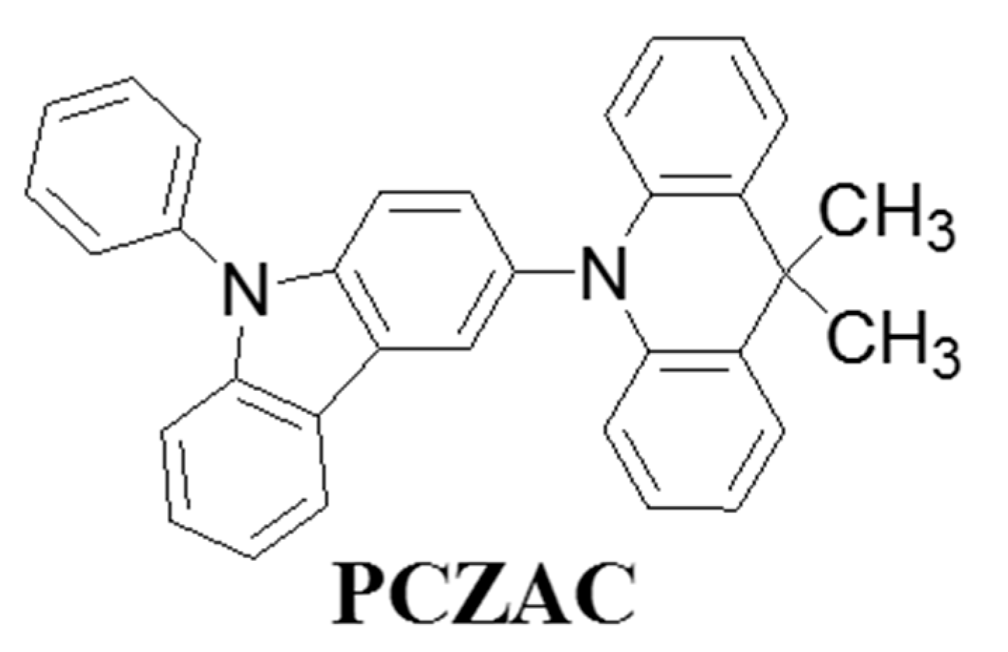
| PCZAC | 2.99 | 3.35 | 5.71 | −2.36 | - | - | [74] |
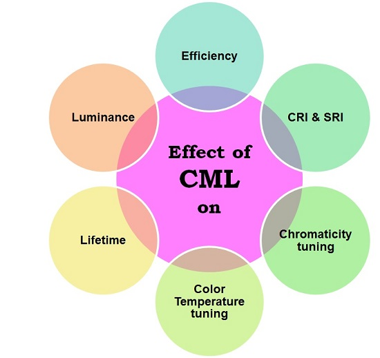
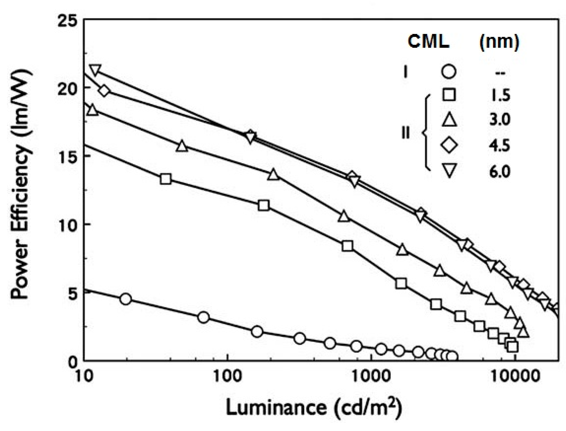
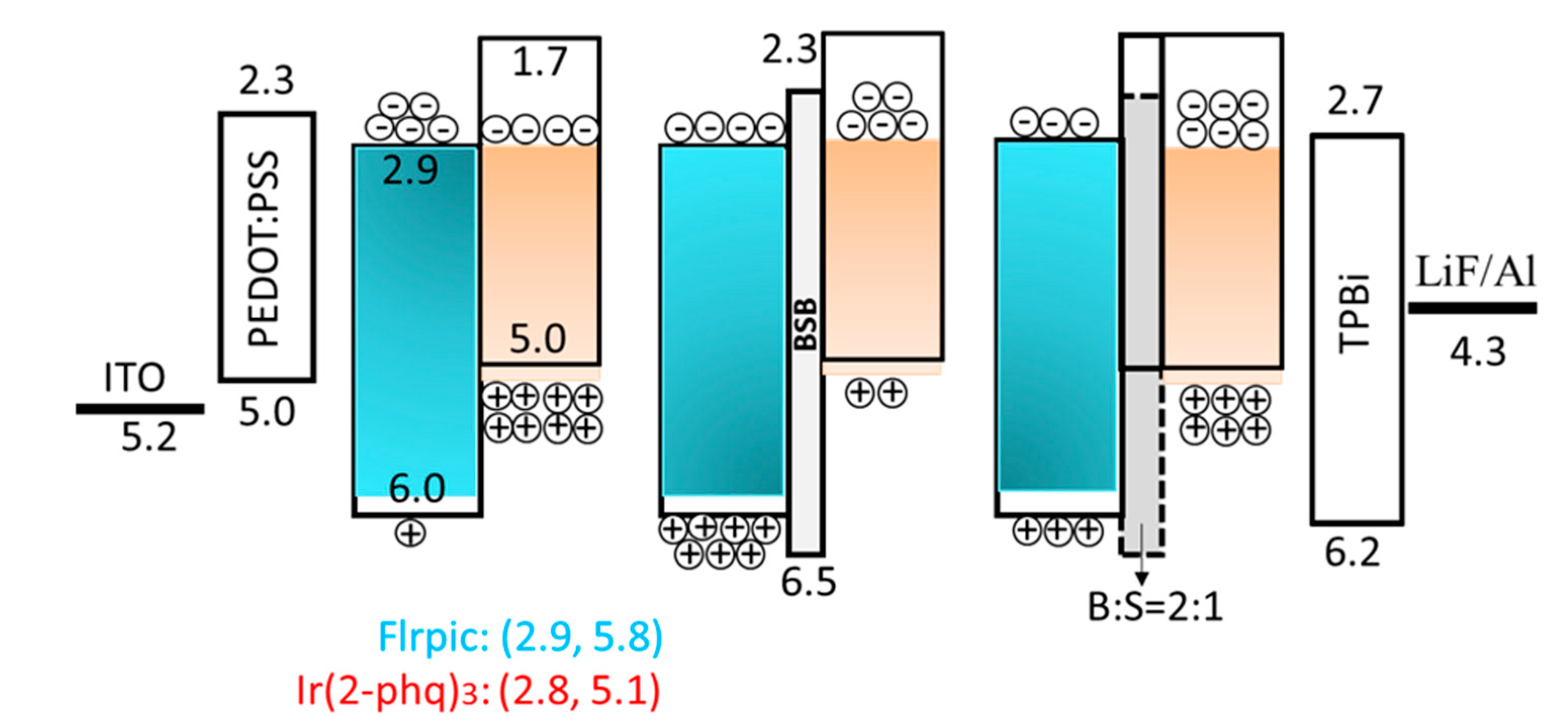
2. Effect of CML on Luminance and Efficiency


3. Effect of CML on Lifetime
4. Effect of CML on CRI and SRI


5. Effect of CML on Chromaticity Tuning


6. Effect of CML on CT Tuning


7. Conclusions
Acknowledgments
Author Contributions
Conflicts of Interest
References
- So, F.; Kido, J.; Burrows, P. Organic light-emitting devices for solid-state lighting. MRS Bull. 2008, 33, 663–669. [Google Scholar] [CrossRef]
- Farinola, G.M.; Ragni, R. Electroluminescent materials for white organic light emitting diodes. Chem. Soc. Rev. 2011, 40, 3467–3482. [Google Scholar] [CrossRef] [PubMed]
- Kido, J.; Okamoto, Y. Organo lanthanide metal complexes for electroluminescent materials. Chem. Rev. 2002, 102, 2357–2368. [Google Scholar] [CrossRef] [PubMed]
- Ulbricht, C.; Beyer, B.; Friebe, C.; Winter, A.; Schubert, U.S. Recent developments in the application of phosphorescent Iridium (III) complex systems. Adv. Mater. 2009, 21, 4418–4441. [Google Scholar] [CrossRef]
- Zhong, C.; Duan, C.; Huang, F.; Wu, H.; Cao, Y. Materials and devices toward fully solution processable organic light-emitting diodes. Chem. Mater. Rev. 2011, 23, 326–340. [Google Scholar] [CrossRef]
- Sasabe, H.; Takamatsu, J.; Motoyama, T.; Watanabe, S.; Wagenblast, G.; Langer, N.; Molt, O.; Fuchs, E.; Lennartz, C.; Kido, J. High-efficiency blue and white organic light-emitting devices incorporating a blue iridium carbene complex. Adv. Mater. 2010, 22, 5003–5007. [Google Scholar] [CrossRef] [PubMed]
- LG launches 77′′,65′′ and 55′′ 4K and FHD OLED TVs in Korea. Available online: http://www.oled-info.com/lg-launches-77-65-and-55-4k-and-fhd-oled-tvs-korea (accessed on 28 May 2015).
- Jou, J.H.; Kumar, S.; Agrawal, A.; Li, T.H.; Sahoo, S. Approaches for fabricating high efficiency organic light emitting diodes. J. Mater. Chem. C 2015, 3, 2974–3002. [Google Scholar] [CrossRef]
- Scechrist, S. TVs, 3-D, and holograms at display week 2014. Inf. Disp. Mag. SID 2014, 30, 14–18. [Google Scholar]
- LG Display can Make 110′′ OLEDs, yields Increase, more Chinese OLED TVs Expected. Available online: http://www.oled-info.com/lg-display-can-make-110-oleds-yields-increase (accessed on 28 May 2015).
- Service, R.F. Organic LEDs look forward to a bright, white future. Science 2005, 310, 1762–1763. [Google Scholar] [CrossRef] [PubMed]
- Zhou, G.J.; Wang, Q.; Ho, C.L.; Wong, W.Y.; Ma, D.G.; Wang, L.X. Duplicating sunlight from simple WOLEDs for lighting application. Chem. Commun. 2009, 24, 3574–3576. [Google Scholar] [CrossRef] [PubMed]
- Zhou, G.J.; Wang, Q.; Wang, X.Z.; Ho, C.L.; Wong, W.Y.; Ma, D.G.; Wang, L.X.; Lin, Z.Y. Metallophosphors of platinum with distinct main-group elements: A versatile approach towards color tuning and white-light emission with superior efficiency/color quality/brightness trade-offs. J. Mater. Chem. 2010, 20, 7472–7484. [Google Scholar] [CrossRef]
- International Energy Agency. Light’s Labour’s Lost, Policies for Energy-Efficient Lighting; IEA Publications: Paris, France, 2006. [Google Scholar]
- Sasabe, H.; Kido, J. Development of high performance OLEDs for general lighting. J. Mater. Chem. C 2013, 1, 1699–1707. [Google Scholar] [CrossRef]
- Sun, Y.; Forrest, S.R. Enhanced light out-coupling of organic light-emitting devices using embedded low-index grids. Nat. Photonics 2008, 2, 483–487. [Google Scholar] [CrossRef]
- He, G.F.; Rothe, C.; Murano, S.; Werner, A.; Zeika, O.; Birnstock, J. White stacked OLED with 38 lm/W and 100,000-hour lifetime at 1000 cd/m2 for display and lighting applications. J. Soc. Inf. Disp. 2009, 17, 159–165. [Google Scholar] [CrossRef]
- Bardsley, N.; Bland, S.; Pattison, L.; Pattison, M.; Stober, K.; Welsh, F.; Yamada, M. Solid-State Lighting Research and Development: Multi-Year Program Plan; No. DOE/EE-1089; Building Technologies Office, Office of Energy Efficiency and Renewable Energy, U.S. Department of Energy: Washington, DC, USA, April 2014; (Updated May 2014). Available online: http://apps1.eere.energy.gov/buildings/publications/pdfs/ssl/ssl_mypp2014_web.pdf (accessed on 1 June 2015).
- Reineke, S.; Lindner, F.; Schwartz, G.; Seidler, N.; Walzer, K.; Lüssem, B.; Leo, K. White organic light emitting diodes with fluorescent tube efficiency. Nature 2009, 459, 234–238. [Google Scholar] [CrossRef] [PubMed]
- Zhou, X.; Blochwitz, J.; Pfeiffer, M.; Nollau, A.; Fritz, T.; Leo, K. Enhanced hole injection into amorphous hole-transport layers of organic light-emitting diodes using controlled p-type doping. Adv. Funct. Mater. 2001, 11, 310–314. [Google Scholar] [CrossRef]
- Huang, J.; Pfeiffer, M.; Werner, A.; Blochwitz, J.; Leo, K.; Liu, S. Low-voltage organic electroluminescent devices using p-i-n structures. Appl. Phys. Lett. 2002, 80, 139–141. [Google Scholar] [CrossRef]
- Pfeiffer, M.; Forrest, S.R.; Leo, K.; Thompson, M.E. Electrophosphorescent p-i-n organic light-emitting devices for very-high-efficiency flat-panel displays. Adv. Mater. 2002, 14, 1633–1636. [Google Scholar] [CrossRef]
- D’Andrade, B.W.; Forrest, S.R.; Chwang, A.B. Operational stability of electrophosphorescent devices containing p and n doped transport layers. Appl. Phys. Lett. 2003, 83, 3858. [Google Scholar] [CrossRef]
- He, G.; Schneider, O.; Qin, D.; Zhou, X.; Pfeiffer, M.; Leo, K. Very high-efficiency and low voltage phosphorescent organic light-emitting diodes based on a p-i-n junction. J. Appl. Phys. 2004, 95, 5773–5777. [Google Scholar] [CrossRef]
- Choudhury, K.R.; Yoon, J.; So, F. LiF as an n-dopant in tris(8-hydroxyquinoline) aluminum thin films. Adv. Mater. 2008, 20, 1456–1461. [Google Scholar] [CrossRef]
- Yook, K.S.; Jeon, S.O.; Min, S.Y.; Lee, J.Y.; Yang, H.J.; Noh, T.; Kang, S.K.; Lee, T.W. Highly efficient p-i-n and tandem organic light emitting devices using an air-stable and low temperature-evaporable metal azide as an n-dopant. Adv. Funct. Mater. 2010, 20, 1797–1802. [Google Scholar] [CrossRef]
- Wang, Q.; Tao, Y.; Qiao, X.; Chen, J.; Ma, D.; Yang, C.; Qin, J. High-performance, phosphorescent, top-emitting organic light-emitting diodes with p-i-n homo junctions. Adv. Funct. Mater. 2011, 21, 1681–1686. [Google Scholar] [CrossRef]
- Hung, L.S.; Tang, C.W.; Mason, M.G. Enhanced electron injection in organic electroluminescence devices using an Al/LiF electrode. Appl. Phys. Lett. 1997, 70, 152. [Google Scholar] [CrossRef]
- Shaheen, S.E.; Jabbour, G.E.; Morrell, M.M.; Kawabe, Y.; Kippelen, B.; Peyghambarian, N. Bright blue organic light-emitting diode with improved color purity using a LiF/Al cathode. J. Appl. Phys. 1998, 84, 2324–2327. [Google Scholar] [CrossRef]
- Jou, J.H.; Chiang, P.H.; Lin, Y.P.; Chang, C.Y.; Lai, C.L. Hole-transporting-layer-free high-efficiency fluorescent blue organic light-emitting diodes. Appl. Phys. Lett. 2007, 91, 043504. [Google Scholar] [CrossRef]
- Jou, J.H.; Wang, Y.S.; Lin, C.H.; Shen, S.M.; Chen, P.C.; Tang, M.C.; Wei, Y.; Tsai, F.Y.; Chen, C.T. Nearly non-roll-off high efficiency fluorescent yellow organic light-emitting diodes. J. Mater. Chem. 2011, 21, 12613–12618. [Google Scholar] [CrossRef]
- Jou, J.H.; Chen, P.C.; Tang, M.C.; Wang, Y.S.; Lin, C.H.; Chen, S.H.; Chen, C.C.; Wang, C.C.; Chen, C.T. Organic light-emitting diodes with rollup character. J. Photonics Energy 2012, 2, 021208. [Google Scholar] [CrossRef]
- Li, H.Y.; Zhou, L.; Teng, M.Y.; Xu, Q.L.; Lin, C.; Zheng, Y.X.; Zuo, J.L.; Zhang, H.J.; You, X.Z. Highly efficient green phosphorescent OLEDs based on a novel iridium complex. J. Mater. Chem. C 2013, 1, 560–565. [Google Scholar] [CrossRef]
- Jou, J.H.; Chen, C.H.; Tseng, J.R.; Peng, S.H.; Chen, P.W.; Chiang, C.I.; Jou, Y.C.; Hong, J.H.; Wang, C.C.; Chen, C.C.; et al. Using light-emitting dyes as a co-host to markedly improve efficiency roll-off in phosphorescent yellow organic light emitting diodes. J. Mater. Chem. C 2013, 1, 394–400. [Google Scholar] [CrossRef]
- Holmes, R.J.; Forrest, S.R.; Tung, Y.J.; Kwong, R.C.; Brown, J.J.; Garon, S.; Thompson, M.E. Blue organic electrophosphorescence using exothermic host–guest energy transfer. Appl. Phys. Lett. 2003, 82, 2422–2424. [Google Scholar] [CrossRef]
- Tsai, M.H.; Hong, Y.H.; Chang, C.H.; Su, H.C.; Wu, C.C.; Matoliukstyte, A.; Simokaitiene, J.; Grigalevicius, S.; Grazulevicius, J.V.; Hsu, C.P. 3-(9-Carbazolyl)carbazoles and 3,6-di(9-carbazolyl)carbazoles as effective host materials for efficient blue organic electrophosphorescence. Adv. Mater. 2007, 19, 862–866. [Google Scholar] [CrossRef]
- Jou, J.H.; Lin, Y.P.; Hsu, M.F.; Wu, M.H.; Lu, P. High efficiency deep-blue organic light-emitting diode with a blue dye in low-polarity host. Appl. Phys. Lett. 2008, 92. [Google Scholar] [CrossRef]
- Choulis, S.A.; Choong, V.E.; Patwardhan, A.; Mathai, M.K.; So, F. Interface modification to improve hole-injection properties in organic electronic devices. Adv. Funct. Mater. 2006, 16, 1075–1080. [Google Scholar] [CrossRef]
- Hughes, G.; Bryce, M.R. Electron-transporting materials for organic electroluminescent and electrophosphorescent devices. J. Mater. Chem. 2005, 15, 94–107. [Google Scholar] [CrossRef]
- Cheng, C.H.; Chou, H.H. A highly efficient universal bipolar host for blue, green, and red phosphorescent OLEDs. Adv. Mater. 2010, 22, 2468–2471. [Google Scholar]
- Jou, J.H.; Tseng, J.R.; Tseng, K.Y.; Wang, W.B.; Jou, Y.C.; Shen, S.M.; Chen, Y.L.; Hung, W.Y.; Chen, S.Z.; Ding, T.Y.; et al. High-efficiency host free deep-blue organic light-emitting diode with double carrier regulating layers. Org. Electron. 2012, 13, 2893–2897. [Google Scholar] [CrossRef]
- Wang, Q.; Ho, C.L.; Zhao, Y.; Ma, D.; Wong, W.Y.; Wang, L. Reduced efficiency roll-off in highly efficient and color-stable hybrid WOLEDs: The influence of triplet transfer and charge-transport behavior on enhancing device performance. Org. Electron. 2010, 11, 238–246. [Google Scholar] [CrossRef]
- Seo, J.H.; Park, J.S.; Lee, S.J.; Seo, B.M.; Lee, K.H.; Park, J.K.; Yoon, S.S.; Kim, Y.K. Codoped spacer ratio effect on EL characteristics of hybrid white organic light-emitting diodes for reduced efficiency roll-off. Jpn. J. Appl. Phys. 2010, 49, 090203. [Google Scholar] [CrossRef]
- Seo, J.H.; Park, J.S.; Lee, S.J.; Seo, B.M.; Lee, K.H.; Park, J.K.; Yoon, S.S.; Kim, Y.K. Codoped spacer ratio effect of hybrid white organic light emitting diodes. Curr. Appl. Phys. 2011, 11, 564–567. [Google Scholar] [CrossRef]
- Reineke, S.; Schwartz, G.; Leo, K. Reduced efficiency roll-off in phosphorescent organic light emitting diodes by suppression of triplet-triplet annihilation. Appl. Phys. Lett. 2007, 91, 123508. [Google Scholar] [CrossRef]
- Sun, Y.; Giebink, N.C.; Kanno, H.; Ma, B.; Thompson, M.E.; Forrest, S.R. Management of singlet and triplet excitons for efficient white organic light-emitting devices. Nat. Lond. 2006, 440, 908–912. [Google Scholar] [CrossRef] [PubMed]
- Jou, J.H.; Hsieh, C.Y.; Tseng, J.R.; Peng, S.H.; Jou, Y.C.; Hong, J.H.; Shen, S.M.; Tang, M.C.; Chen, P.C.; Lin, C.H. Candle light-style OLEDs. Adv. Funct. Mater. 2013, 23, 2750–2757. [Google Scholar] [CrossRef]
- Seo, J.H.; Park, H.; Kim, G.Y.; Lee, K.H.; Kim, M.K.; Yoon, S.S.; Kim, Y.K. Hybrid spacer for high-efficiency white organic-light-emitting diodes. Appl. Phys. Lett. 2008. [Google Scholar] [CrossRef]
- Wang, Y.; Hua, Y.; Wu, X.; Zhang, L.; Hou, Q.; Zhang, N.; Ma, L.; Cheng, X.; Yin, S. Application of mixed interface in white-electrophosphorescent devices: An efficient approach to adjust the distributions of carriers. Appl. Phys. Lett. 2008, 93, 113302. [Google Scholar] [CrossRef]
- Schwarts, G.; Fehse, K.; Pfeiffer, M.; Walzer, K.; Leo, K. Highly efficient white organic light emitting diodes comprising an interlayer to separate fluorescent and phosphorescent regions. Appl. Phys. Lett. 2006, 89, 083509. [Google Scholar] [CrossRef]
- Zhao, F.; Sun, N.; Zhang, H.; Chen, J.; Ma, D. Hybrid white organic light-emitting diode with a double light-emitting layer structure for high color-rendering index. J. Appl. Phys. 2012, 112, 084504. [Google Scholar] [CrossRef]
- Zhao, F.; Zhang, Z.; Liu, Y.; Dai, Y.; Chen, J.; Ma, D. A hybrid white organic light emitting diodes with stable color and reduced efficiency roll-off by using a bipolar charge carrier switch. Org. Electron. 2012, 13, 1049–1055. [Google Scholar] [CrossRef]
- Jou, J.H.; Chen, S.H.; Shen, S.M.; Jou, Y.C.; Lin, C.H.; Peng, S.H.; Hsia, S.P.; Wang, C.W.; Chen, C.C.; Wang, C.C. High efficiency low color-temperature organic light emitting diodes with a blend interlayer. J. Mater. Chem. 2011, 21, 17850–17854. [Google Scholar] [CrossRef]
- Seo, J.H.; Park, J.S.; Koo, J.R.; Lee, S.J.; Seo, B.M.; Lee, K.H.; Park, J.K.; Yoon, S.S.; Kim, Y.K. Ratio effect of codoped spacer on electroluminescent characteristics of hybrid white organic light-emitting diodes. Jpn. J. Appl. Phys. 2010, 49, 042104. [Google Scholar] [CrossRef]
- Seo, J.H.; Park, J.S.; Koo, J.R.; Lee, S.J.; Seo, B.M.; Lee, K.H.; Yoon, S.S.; Kim, Y.K. Mixed spacer effect of hybrid white organic light-emitting diodes for reduced efficiency roll-off. In Proceedings of the 2010 3rd International Nanoelectronics Conference (INEC), Hong Kong, China, 3–8 January 2010; pp. 1220–1221.
- Leem, D.S.; Kim, J.W.; Jung, S.O.; Kim, S.O.; Kim, S.H.; Kim, K.Y.; Kim, Y.H.; Kwon, S.K.; Kim, J.J. Efficient and colour-stable hybrid white organic light-emitting diodes utilizing electron-hole balanced spacers. J. Phys. D Appl. Phys. 2010, 43, 405102–405107. [Google Scholar] [CrossRef]
- Kang, J.W.; Lee, S.H.; Park, H.D.; Jeong, W.I.; Yoo, K.M.; Park, Y.S.; Kim, J.J. Low roll-off of efficiency at high current density in phosphorescent organic light emitting diodes. Appl. Phys. Lett. 2007, 90, 223508. [Google Scholar] [CrossRef]
- Jou, J.H.; Kumar, S.; Fang, P.H.; Venkateswararao, A.; Thomas, K.R. J.; Shyue, J.J.; Wang, Y.C.; Li, T.H.; Yu, H.H. Highly efficient ultra-deep blue organic light-emitting diodes with a wet- and dry-process feasible cyanofluorene acetylene based emitter. J. Mater. Chem. C 2015, 3, 2182–2194. [Google Scholar] [CrossRef]
- Lehnhardt, M.; Hamwi, S.; Hoping, M.; Reinker, J.; Riedl, T.; Kowalsky, W. Charge carrier densities in chemically doped organic semiconductors verified by two independent techniques. Appl. Phys. Lett. 2010, 96, 193301. [Google Scholar] [CrossRef]
- Zhang, X.; Shen, W.; Zhang, D.; Zheng, Y.; Hea, R.; Li, M. Theoretical investigation of dihydroacridine and diphenylsulphone derivatives as thermally activated delayed fluorescence emitters for organic light-emitting diodes. RSC Adv. 2015, 5, 51586–51591. [Google Scholar] [CrossRef]
- Deng, Z.; Lee, S.T.; Webb, D.P.; Chan, Y.C.; Gambling, W.A. Carrier transport in thin films of organic electroluminescent materials. Synth. Met. 1999, 107, 107–109. [Google Scholar] [CrossRef]
- Hung, W.Y.; Ke, T.H.; Lin, Y.T.; Wu, C.C.; Hung, T.H.; Chao, T.C.; Wong, K.T.; Wu, C.I. Employing ambipolar oligofluorene as the charge-generation layer in time-of-flight mobility measurements of organic thin films. Appl. Phys. Lett. 2006, 88, 064102. [Google Scholar] [CrossRef]
- Xin, Q.; Li, W.L.; Su, W.M.; Li, T.L.; Su, Z.S.; Chu, B.; Li, B. Emission mechanism in organic light-emitting devices comprising a europium complex as emitter and an electron transporting material as host. J. Appl. Phys. 2007, 101, 044512:1–044512:6. [Google Scholar] [CrossRef]
- Li, Y.Q.; Fung, M.K.; Xie, Z.; Lee, S.T.; Hung, L.S.; Shi, J. An efficient pure blue organic light-emitting device with low driving voltages. Adv. Mater. 2002, 14, 1317–1321. [Google Scholar] [CrossRef]
- Naka, S.; Okada, H.; Onnagawa, H.; Tsutsui, T. High electron mobility in bathophenanthroline. Appl. Phys. Lett. 2000, 76, 197–199. [Google Scholar] [CrossRef]
- Chen, H.F.; Yang, S.J.; Tsai, Z.H.; Hung, W.Y.; Wang, T.C.; Wong, K.T. 1,3,5-Triazine derivatives as new electron transport-type host materials for highly efficient green phosphorescent OLEDs. J. Mater. Chem. 2009, 19, 8112–8118. [Google Scholar] [CrossRef]
- Tanaka, D.; Takeda, T.; Chiba, T.; Watanabe, S.; Kido, J. Novel electron-transport material containing boron atom with a high triplet excited energy level. Chem. Lett. 2007, 36, 262–263. [Google Scholar] [CrossRef]
- Yua, J.; Yin, Y.; Liu, W.; Zhang, W.; Zhang, L.; Xie, W.; Zhao, H. Effect of the greenish-yellow emission on the color rendering index of white organic light-emitting devices. Org. Electron. 2014, 15, 2817–2821. [Google Scholar] [CrossRef]
- Kang, J.W.; Lee, D.S.; Park, H.D.; Park, Y.S.; Kim, J.W.; Jeong, W.I.; Yoo, K.M.K.; Go, K.; Kim, S.H.; Kim, J.J. Silane- and triazine-containing hole and exciton blocking material for high-efficiency phosphorescent organic light emitting diodes. J. Mater. Chem. 2007, 17, 3714–3719. [Google Scholar] [CrossRef]
- Pu, Y.J.; Nakata, G.; Satoh, F.; Sasabe, H.; Yokoyama, D.; Kido, J. Optimizing the charge balance of fluorescent organic light-emitting devices to achieve high external quantum efficiency beyond the conventional upper limit. Adv. Mater. 2012, 24, 1765–1770. [Google Scholar] [CrossRef] [PubMed]
- Strohriegl, P.; Grazulevicius, J.V. Charge-transporting molecular glasses. Adv. Mater. 2002, 14, 1439–1452. [Google Scholar] [CrossRef]
- Schwartz, G.; Pfeiffer, M.; Walzer, K.; Leo, K. Harvesting triplet excitons from fluorescent blue emitters for high-efficiency white organic light emitting diodes. Proc. SPIE 2007, 6655, 66550J. [Google Scholar]
- Kim, S.H.; Jang, J.; Lee, J.Y. High efficiency phosphorescent organic light-emitting diodes using carbazole-type triplet exciton blocking layer. Appl. Phys. Lett. 2007, 90. [Google Scholar] [CrossRef]
- Seo, J.A.; Jeon, S.K.; Gong, M.S.; Lee, J.Y.; Noh, C.H.; Kim, S.H. Long lifetime blue phosphorescent organic light emitting diodes with an exciton blocking layer. J. Mater. Chem. C 2015, 3, 4640–4645. [Google Scholar] [CrossRef]
- Jou, J.H.; Chou, K.Y.; Yang, F.C.; Hsieh, C.H.; Kumar, S.; Agrawal, A.; Chen, S.Z.; Li, T.H.; Yu, H.H. Pseudo-natural light for displays and lighting. Adv. Opt. Mater. 2015, 3, 95–102. [Google Scholar] [CrossRef]
- Jou, J.H.; Chou, K.Y.; Yang, F.C.; Agrawal, A.; Chen, S.Z.; Tseng, J.R.; Lin, C.C.; Chen, P.W.; Wong, K.T.; Chi, Y. A universal, easy-to-apply light-quality index based on natural light spectrum resemblance. Appl. Phys. Lett. 2014, 104, 203304:1–203304:5. [Google Scholar] [CrossRef]
- D’Andrade, B.W.; Thompson, M.E.; Forrest, S.R. Controlling exciton diffusion in multilayer white phosphorescent organic light emitting devices. Adv. Mater. 2002, 14, 147–151. [Google Scholar] [CrossRef]
- Chen, P.; Xie, W.; Li, J.; Guan, T.; Duan, Y.; Zhao, Y.; Liu, S.; Ma, C. White organic light-emitting devices with a bipolar transport layer between blue fluorescent and orange phosphorescent emitting layers. Appl. Phys. Lett. 2007, 91, 023505. [Google Scholar] [CrossRef]
- Park, J.H.; Kim, G.Y.; Lee, S.J.; Seo, J.H.; Seo, J.H.; Kim, Y.K. White organic light emitting diodes using red and blue phosphorescent materials with blocking layer. Trans. Electr. Electron. Mater. 2007, 8, 218–221. [Google Scholar]
- Ho, C.L.; Lin, M.F.; Wong, W.Y.; Wong, W.K.; Chen, C.H. High-efficiency and color-stable white organic light-emitting devices based on sky blue electrofluorescence and orange electrophosphorescence. Appl. Phys. Lett. 2008, 92, 083301:1–083301:3. [Google Scholar] [CrossRef]
- Wang, Q.; Yu, J.; Zhao, J.; Li, M.; Lu, Z. Enhancement of charge carrier recombination efficiency by utilizing a hole-blocking interlayer in white OLEDs. J. Phys. D Appl. Phys. 2013, 46, 155102:1–155102:7. [Google Scholar] [CrossRef]
- Kim, J.Y.; Kim, N.H.; Kim, J.W.; Kang, J.S.; Yoon, J.A.; Yoo, S.I.; Kim, W.Y.; Cheah, K.W. Enhancement of external quantum efficiency and reduction of roll-off in blue phosphorescent organic light emitting diodes using TCTA inter-layer. Opt. Mater. 2014, 37, 120–124. [Google Scholar] [CrossRef]
- Jou, J.H.; Shen, S.M.; Wu, M.H.; Peng, S.H.; Wang, H.C. Sunlight-style organic light-emitting diodes. J. Photonics Energy 2011, 1, 011021:1–011021:5. [Google Scholar] [CrossRef]
- Jou, J.H.; Chen, P.W.; Chen, Y.L.; Jou, Y.C.; Tseng, J.R.; Wu, R.Z.; Hsieh, C.Y.; Hsieh, Y.C.; Joers, P.; Chen, S.H.; et al. OLEDs with chromaticity tunable between dusk-hue and candle-light. Org. Electron. 2013, 14, 47–54. [Google Scholar] [CrossRef]
- Jou, J.H.; Wang, H.C.; Shen, S.M.; Peng, S.H.; Wu, M.H.; Chen, S.H.; Wu, P.H. Highly efficient color-temperature tunable organic light emitting diodes. J. Mater. Chem. 2012, 22, 8117–8120. [Google Scholar] [CrossRef]
- Jou, J.H.; Wu, M.H.; Shen, S.M.; Wang, H.C.; Chen, S.Z.; Chen, S.H.; Lin, C.R.; Hsieh, Y.L. Sunlight-style color-temperature tunable organic light-emitting diode. Appl. Phys. Lett. 2009, 95, 013307. [Google Scholar] [CrossRef]
- Murawski, C.; Leo, K.; Gather, M.C. Efficiency roll-off in organic light-emitting diodes. Adv. Mater. 2013, 25, 6801–6827. [Google Scholar] [CrossRef] [PubMed]
- Kawamura, Y.; Brooks, J.; Brown, J.J.; Sasabe, H.; Adachi, C. Intermolecular interaction and a concentration-quenching mechanism of phosphorescent Ir(III) complexes in a solid film. Phys. Rev. Lett. 2006, 96, 17404. [Google Scholar] [CrossRef]
- Reineke, S.; Rosenow, T.C.; Lüssem, B.; Leo, K. Improved high-brightness efficiency of phosphorescent organic LEDs comprising emitter molecules with small permanent dipole moments. Adv. Mater. 2010, 22, 3189–3193. [Google Scholar] [CrossRef] [PubMed]
- Park, N.G.; Choi, G.C.; Lee, Y.H.; Kim, Y.S. Theoretical studies on the ground and excited states of blue phosphorescent cyclometalated Ir(III) complexes having ancillary ligand. Curr. Appl. Phys. 2006, 6, 620–626. [Google Scholar] [CrossRef]
- Sasabe, H.; Gonmori, E.; Chiba, T.; Li, Y.J.; Tanaka, D.; Su, S.J.; Takeda, T.; Pu, Y.J.; Kido, J.; Nakayama, K.I. Wide-energy-gap electron-transport materials containing 3,5-dipyridylphenyl moieties for an ultra-high efficiency blue organic light-emitting device. J. Chem. Mater. 2008, 20, 5951–5953. [Google Scholar] [CrossRef]
- Koene, B.E.; Loy, D.E.; Thompson, M.E. Asymmetric triaryldiamines as thermally stable hole transporting layers for organic light-emitting devices. Chem. Mater. 1998, 10, 2235–2250. [Google Scholar] [CrossRef]
- Huang, Q.; Evmenenko, G.A.; Dutta, P.; Lee, P.; Armstrong, N.R.; Marks, T.J. Covalently bound hole-injecting nanostructures. Systematics of molecular architecture, thickness, saturation, and electron-blocking characteristics on organic light-emitting diode luminance, turn-on voltage, and quantum efficiency. J. Am. Chem. Soc. 2005, 127, 10227–10242. [Google Scholar] [CrossRef] [PubMed]
- Zhang, Y.; Whited, M.; Thompson, M.E.; Forrest, S.R. Singlet-triplet quenching in high intensity fluorescent organic light emitting diodes. Chem. Phys. Lett. 2010, 495, 161–165. [Google Scholar] [CrossRef]
- Zhang, Y.; Slootsky, M.; Forrest, S.R. Enhanced efficiency in high-brightness fluorescent organic light emitting diodes through triplet management. Appl. Phys. Lett. 2011, 99, 223303. [Google Scholar] [CrossRef]
- Giebink, N.; Forrest, S.R. Quantum efficiency roll-off at high brightness in fluorescent and phosphorescent organic light emitting diodes. Phys. Rev. B 2008, 77, 235215. [Google Scholar] [CrossRef]
- Van Mensfoort, S.L.M.; Carvelli, M.; Megens, M.; Wehenkel, D.; Bartyzel, M.; Greiner, H.; Janssen, R.A.J.; Coehoorn, R. Measuring the light emission profile in organic light-emitting diodes with nanometer spatial resolution. Nat. Photonics 2010, 4, 329–335. [Google Scholar] [CrossRef]
- Lee, J.; Lee, J.I.; Lee, J.Y.; Chu, H.Y. Stable efficiency roll-off in blue phosphorescent organic light-emitting diodes by host layer engineering. Org. Electron. 2009, 10, 1529–1533. [Google Scholar] [CrossRef]
- Chin, B.D. Enhancement of efficiency and stability of phosphorescent OLEDs based on heterostructured light-emitting layers. J. Phys. D Appl. Phys. 2011, 44, 115103. [Google Scholar] [CrossRef]
- Hudson, Z.M.; Wang, Z.; Helander, M.G.; Lu, Z.H.; Wang, S. N-heterocyclic carbazole-based hosts for simplified single-layer phosphorescent OLEDs with high efficiencies. Adv. Mater. 2012, 24, 2922–2928. [Google Scholar] [PubMed]
- Jou, J.H.; Kumar, S.; Jou, Y.C. Disruptive characteristics and lifetime issues of organic light emitting diodes. In Organic Light-Emitting Diodes (OLEDs): Materials, Devices and Applications, 1st ed.; Buckley, A., Ed.; Woodhead Publishing Ltd: Cambridge, UK, 2012; pp. 410–442. [Google Scholar]
- Kalinowski, J.; Stampor, W.; Cocchi, M.; Virgili, D.; Fattori, V.; Marco, P.D. Triplet energy exchange between fluorescent and phosphorescent organic molecules in a solid state matrix. Chem. Phys. 2004, 297, 39–48. [Google Scholar] [CrossRef]
- Chen, P.; Xue, Q.; Xie, W.; Xie, G.; Duan, Y.; Zhao, Y.; Liu, S.; Zhang, L.; Lin, B. Influence of interlayer on the performance of stacked white organic light-emitting devices. Appl. Phys. Lett. 2009, 95, 123307. [Google Scholar] [CrossRef]
- Yook, K.S.; Lee, J.Y. Effect of the interlayer composition on the lifetime and color change of hybrid white organic light-emitting diodes. J. Ind. Eng. Chem. 2011, 17, 642–644. [Google Scholar] [CrossRef]
- VanSlyke, S.A.; Chen, C.H.; Tang, C.W. Organic electroluminescent devices with improved stability. Appl. Phys. Lett. 1996, 69, 2160. [Google Scholar] [CrossRef]
- Aziz, H.; Luo, Y.; Xu, G.; Popovic, Z.D. Improving the stability of organic light-emitting devices by using a thin Mg anode buffer layer. Appl. Phys. Lett. 2006, 89, 103515. [Google Scholar] [CrossRef]
- Liu, B.; Wang, L.; Xu, M.; Tao, H.; Zou, J.; Gao, D.; Lan, L.; Ning, H.; Peng, J.; Liu, Y.C. Efficient hybrid white organic light-emitting diodes with extremely long lifetime: The effect of n-type interlayer. Sci. Rep. 2014, 4, 7198. [Google Scholar] [CrossRef] [PubMed]
- Lee, S.J.; Lee, S.E.; Lee, D.H.; Koo, J.R.; Lee, H.W.; Yoon, S.S.; Park, J.; Kim, Y.K. Effect of broad recombination zone in multiple quantum well structures on lifetime and efficiency of blue organic light-emitting diodes. Jpn. J. Appl. Phys. 2014, 53, 101601. [Google Scholar] [CrossRef]
- Niu, X.; Ma, L.; Yao, B.; Ding, J.; Tu, G.; Xie, Z.; Wang, L. White polymeric light-emitting diodes with high color rendering index. Appl. Phys. Lett. 2006, 89, 213508. [Google Scholar] [CrossRef]
- Kalinowski, J.; Cocchi, M.; Virgili, D.; Fattori, V.; Williams, J.A.G. Mixing of excimer and exciplex emission: A new way to improve white light emitting organic electrophosphorescent diodes. Adv. Mater. 2007, 19, 4000–4005. [Google Scholar] [CrossRef]
- Yang, H.; Shi, Y.; Zhao, Y.; Meng, Y.; Hu, W.; Hou, J.; Liu, S. High colour rendering index white organic light-emitting devices with three emitting layers. Displays 2008, 29, 327–332. [Google Scholar] [CrossRef]
- Chang, C.H.; Tien, K.C.; Chen, C.C.; Lin, M.S.; Cheng, H.C.; Liu, S.H.; Wu, C.C.; Hung, J.Y.; Chiu, Y.C.; Chi, Y. Efficient phosphorescent white OLEDs with high color rendering capability. Org. Electron. 2010, 11, 412–418. [Google Scholar] [CrossRef]
- Jou, J.H.; Chou, Y.C.; Shen, S.M.; Wu, M.H.; Wu, P.S.; Lin, C.R.; Wu, R.Z.; Chen, S.H.; Wei, M.K.; Wang, C.W. High-efficiency, very-high color rendering white organic light-emitting diode with a high triplet interlayer. J. Mater. Chem. 2011, 21, 18523–18526. [Google Scholar] [CrossRef]
- Jou, J.H.; Shen, S.M.; Lin, C.R.; Wang, Y.S.; Chou, Y.C.; Chen, S.Z.; Jou, Y.C. Efficient very-high color rendering index organic light-emitting diode. Org. Electron. 2011, 12, 865–868. [Google Scholar] [CrossRef]
- Weichsel, C.; Reineke, S.; Furno, M.; Lüssem, B.; Leo, K. Organic light-emitting diodes for lighting: High color quality by controlling energy transfer processes in host-guest-systems. J. Appl. Phys. 2012, 111, 033102. [Google Scholar] [CrossRef]
- Xiong, L.; Zhu, W.; Wei, N.; Li, J.; Sun, W.; Wu, X.; Cao, J.; Wang, Z. High color rendering index and chromatic-stable white organic light emitting diodes incorporating excimer and fluorescence emission. Org. Electron. 2013, 14, 32–37. [Google Scholar] [CrossRef]
- Sun, N.; Zhao, Y.; Zhao, F.; Chen, Y.; Yang, D.; Chen, J.; Ma, D. A white organic light-emitting diode with ultra-high color rendering index, high efficiency, and extremely low efficiency roll-off. Appl. Phys. Lett. 2014, 105, 013303. [Google Scholar] [CrossRef]
- Cocchi, M.; Kalinowski, J.; Virgili, D.; Fattori, V.; Develay, S.J.; Williams, A.G. Single-dopant organic white electrophosphorescent diodes with very high efficiency and its reduced current density roll-off. Appl. Phys. Lett. 2007, 90, 163508. [Google Scholar] [CrossRef]
- Huang, M.H.; Lin, W.C.; Fan, C.C.; Wang, Y.S.; Lin, H.W.; Liao, J.L.; Lin, C.H.; Chi, Y. Tunable chromaticity stability in solution-processed organic light emitting devices. Org. Electron. 2015, 20, 36–42. [Google Scholar] [CrossRef]
- Choukri, H.; Fischer, A.; Forget, S.; Chenais, S.; Billeton, T.; Castex, M.C.; Ades, D.; Siove, A.; Lemaitre, N.; Denis, C. Influence of thickness and position of an ultrathin yellow layer on color tuning (including white) of organic light emitting diode. In Proceedings of the IEEE Industrial Electronics, IECON 2006—32nd Annual Conference, Paris, France, 6–10 November 2006.
- Liao, S.Y.; Kumar, S.; Yu, H.H.; An, C.C.; Wang, Y.C.; Lin, J.W.; Wang, Y.L.; Liu, Y.C.; Wu, C.L.; Jou, J.H. Organic light-emitting diode with color tunable between bluish-white daylight and orange-white dusk hue. Int. J. Photoenergy 2014, 2014, 6. [Google Scholar] [CrossRef]
- Liu, S.; Wu, R.; Huang, J.; Yu, J. Color-tunable and high-efficiency organic light-emitting diode by adjusting exciton bilateral migration zone. Appl. Phys. Lett. 2013, 103, 133307. [Google Scholar] [CrossRef]
- Van Bommel, W.J.M. Non-visual biological effect of lighting and the practical meaning for lighting for work. Appl. Ergon. 2006, 37, 461–466. [Google Scholar] [CrossRef] [PubMed]
- Kuller, R.; Wetterberg, L. Melatonin, cortisol, EEG, ECG and subjective comfort in healthy humans: Impact of two fluorescent lamp types at two light intensities. Light. Res. Technol. 1993, 25, 71–80. [Google Scholar] [CrossRef]
- Mills, P.R.; Tomkins, S.C.; Schlangen, L.J.M. The effect of high correlated colour temperature office lighting on employee wellbeing and work performance. J. Circadian Rhythm. 2007, 5, 1–9. [Google Scholar] [CrossRef] [PubMed]
- Pauley, S.M. Lighting for the human circadian clock: Recent research indicates that lighting has become a public health issue. Med. Hypotheses 2004, 63, 588–596. [Google Scholar] [CrossRef] [PubMed]
- Brainard, G.C.; Richardson, B.A.; King, T.S.; Reiter, R.J. The influence of different light spectra on the suppression of pineal melatonin content in the Syrian hamster. Brain Res. 1984, 294, 333–339. [Google Scholar] [CrossRef]
- Lockley, S.W.; Brainard, G.C.; Czeisler, C.A. High sensitivity of the human circadian melatonin rhythm to resetting by short wavelength light. J. Clin. Endocrinol. Metab. 2003, 88, 4502–4505. [Google Scholar] [CrossRef] [PubMed]
- Scheer, F.A.J.L.; Buijs, R.M. Light affects morning salivary cortisol in humans. J. Clin. Endocrinol. Metab. 1999, 84, 3395–3398. [Google Scholar] [CrossRef] [PubMed]
- Sato, M.; Sakaguchi, T.; Morita, T. The effects of exposure in the morning to light of different color temperatures on the behavior of core temperature and melatonin secretion in humans. Biol. Rhythm. Res. 2005, 36, 287–292. [Google Scholar] [CrossRef]
- Behar-Cohen, F.; Martinsons, C.; Viénot, F.; Zissis, G.; Barlier-Salsi, A.; Cesarini, J.P.; Enouf, O.; Garcia, M.; Picaud, S.; Attia, D. Light-emitting diodes (LED) for domestic lighting: Any risks for the eye? Prog. Retin. Eye Res. 2011, 30, 239–257. [Google Scholar] [CrossRef] [PubMed]
- Jou, J.H.; Kumar, S.; An, C.C.; Singh, M.; Yu, H.H.; Hsieh, C.Y.; Lin, Y.X.; Sung, C.F.; Wang, C.W. Enabling a blue-hazard free general lighting based on candle light-style organic light emitting diode. Opt. Express 2015, 23, A576–A581. [Google Scholar] [CrossRef] [PubMed]
© 2015 by the authors. Licensee MDPI, Basel, Switzerland. This article is an open access article distributed under the terms and conditions of the Creative Commons Attribution license ( http://creativecommons.org/licenses/by/4.0/).
Share and Cite
Jou, J.-H.; Kumar, S.; Singh, M.; Chen, Y.-H.; Chen, C.-C.; Lee, M.-T. Carrier Modulation Layer-Enhanced Organic Light-Emitting Diodes. Molecules 2015, 20, 13005-13030. https://doi.org/10.3390/molecules200713005
Jou J-H, Kumar S, Singh M, Chen Y-H, Chen C-C, Lee M-T. Carrier Modulation Layer-Enhanced Organic Light-Emitting Diodes. Molecules. 2015; 20(7):13005-13030. https://doi.org/10.3390/molecules200713005
Chicago/Turabian StyleJou, Jwo-Huei, Sudhir Kumar, Meenu Singh, Yi-Hong Chen, Chung-Chia Chen, and Meng-Ting Lee. 2015. "Carrier Modulation Layer-Enhanced Organic Light-Emitting Diodes" Molecules 20, no. 7: 13005-13030. https://doi.org/10.3390/molecules200713005