Abstract
The maximum entropy method (MEM) is widely used in research fields such as linguistics, meteorology, physics, and chemistry. Recently, MEM application has become a subject of interest in the semiconductor engineering field, in which devices utilize very thin films composed of many materials. For thin film fabrication, it is essential to thoroughly understand atomic-scale structures, internal fixed charges, and bulk/interface traps, and many experimental techniques have been developed for evaluating these. However, the difficulty in interpreting the data they provide prevents the improvement of device fabrication processes. As a candidate for a very practical data analyzing technique, MEM is a promising approach to solve this problem. In this paper, we review the application of MEM to thin films used in semiconductor engineering. The method provides interesting and important information that cannot be obtained with conventional methods. This paper explains its theoretical background, important points for practical use, and application results.
1. Introduction
The maximum entropy method (MEM), which initially attracted attention from its use in astronomical image restoration, is now used in various research fields such as linguistics, meteorology, and data processing. It has also begun to be applied to spectroscopic data analysis in physics and chemistry. Its use in interpreting X-ray diffraction data has had a particularly significant impact. In this application area, Collins first used MEM to visualize electron density images [1]. Later, the method was widely used to extract very detailed structural information on many compounds, e.g., metallofullerene compounds [2,3,4]. It was also used to reveal hydrogen and oxygen positions [5,6] and even to determine very large protein structures [7]. It should be noted that such structural information cannot be obtained by using the conventional Fourier transform method. This is because this method needs infinite data length, while actual data is finite and furthermore contains noise. This results in ghost peaks and anomalous negative electron density. On the other hand, MEM is tolerant to noise and provides only positive electron density, which enables us to determine the precise position of light elements such as hydrogen. In other MEM application examples, it has been used to extract the decay constant distribution from fluorimetry [8] and to analyze X-ray scattering [9,10], neutron diffraction [11,12] and scattering [13,14]. In such applications it provides very detailed structural information. Recently, it was used to analyze X-ray reflectivity spectra [15]. Ueda et al. showed that MEM can determine film thicknesses more precisely than the conventional Fourier transform method. These studies prove the validity of MEM as a tool to solve the inverse problems that often prevent precise data interpretation.
The application of MEM to semiconductor engineering has also been a subject of great interest. Although not many reports have been issued in this regard, MEM is gradually becoming popular as a powerful analyzing tool. The most popular application in this field may be the extraction of the depth distribution of atoms inside ultrathin films [16,17,18,19,20]. In using MEM to analyze angle resolved X-ray photoelectron spectroscopy (ARXPS) data, Chang et al. reconstructed nitrogen depth distribution in nitrided silicon oxide films (SiON) and concluded that MEM enables nondestructive determination of depth distribution [19]. Moreover, MEM made it possible to determine even the chemical-state-resolved depth distribution [19,20]. This information cannot be obtained using other conventional methods such as medium energy ion scattering or secondary ion mass spectroscopy, which evidences the advantages of MEM. Since the equivalent oxide thickness for semiconductor devices is less than 1 nm, even subtle variance in chemical composition is important for understanding electrical characteristics. In addition, for implementing the new materials called high-k dielectrics, e.g., hafnium oxide, the depth distribution of atoms in the oxide becomes more crucial because a high-k oxide is likely to react with the underlying Si substrate, resulting in silicate layers being formed between the high-k oxide and Si [21]. Although the silicate layers are very thin (several nm at most), they significantly affect properties such as leakage current, traps, interface state, and fixed charges. Therefore, nondestructive and highly sensitive structural determination is becoming increasingly important. For this reason, MEM as an ARXPS data analyzing tool is certain to become more popular and important in the future.
On the other hand, there have been few reports on MEM usage other than for ARXPS data analysis [22,23,24,25]. Semiconductor device characteristics are affected not only by specific atom or chemical species distributions, but also by traps, interface states, and fixed charges present inside films and/or at interfaces between the gate insulator and substrate. For example, they can induce threshold voltage shifts, e.g., negative bias temperature instability and hot carrier injection, or leakage current, e.g., stress-induced leakage current and trap assisted tunneling, through carrier capture/emission events. These events prevent normal operation of devices and it is crucial to take them into account in device development. On the other hand, traps are utilized to accumulate carriers as memory in charge trap flash memory devices. Thus, they are linked more directly to device characteristics than depth distribution and detailed information about them is strongly required.
Several techniques are generally used to measure electrical characteristics since the characteristics are too subtle to observe with usual spectroscopic detection techniques such as XPS. These techniques include thermally-stimulated-current (TSC), isochronal annealing (IA), and thickness-dependent CV (TDCV). However, their data is difficult to interpret because their analyses are attributed to inverse problems that cannot be solved analytically.
Very recently, MEM was applied to TSC data to determine the density (Nt) and energy level (Et) of traps in SiON thin films [22,23]. The results evidenced that MEM provides detailed Nt(Et) distribution and even its compositional dependence. It was also used to determine the distribution in the gate insulator in metal-oxide-semiconductor field effect transistors (MOSFETs) [24]. The obtained results indicate that more traps are present in smaller gate size MOSFETs, which implies that the gate edges are likely to be damaged during fabrication processes. These results are very informative for improving device fabrication processes and understanding trap physics. A scheme has also been developed for applying MEM to IA and TDCV data analysis to acquire information about fixed charges and interface states as well as traps [25].
This paper describes MEM application to semiconductor engineering techniques, e.g., ARXPS, TSC, IA, and TDCV. The method’s theory, validity, and important points for practical use are explained. Application results obtained for simple metal-oxide-semiconductor (MOS) systems are also presented.
2. Theoretical Examination of MEM
2.1. Theory
2.1.1. General Description of MEM
MEM is a method to reconstruct original data from discrete and finite experimental data sets with noise. For most engineers, its practical equations and important points for using them may be more desirable than its detailed theoretical background (Bayesian theory). Therefore, I explain them through brief basic theoretical examinations. The spectroscopic data of measurement techniques used in the semiconductor engineering field, such as ARXPS, TSC, IA, and TDCV, is expressed by the equation
where , Mn,i, and yi are measured data, a known function including experimental conditions, and the original data one wishes to obtain. Generally, yi is discrete and finite, and includes noise. For an ARXPS example, , Mn,i, and yi correspond to the measured angle dependent signal intensity, a function including the X-ray incident angle and experimental conditions such as the sensitivity factor, and the depth distribution of atoms. Here, n and i are the data point and the distance from the surface of a sample. Since Equation (1) generally cannot be solved, an assumption is required to extract yi, e.g., yi can be approximated by a linear function yi = axi + b, where a and b are constants and xi is the depth from the surface. In this case, since Mn,i is a known function, a and b can be determined from the curve fitting procedure, which provides the depth distribution yi. This fitting method is widely used since it is a very easy and time-saving procedure; however, it requires prior knowledge about the depth distribution function, which is a great disadvantage since it is difficult to determine it in advance. Similarly, when yi is approximated by Gaussian functions, one must determine how many peaks are involved in advance. Thus, the conventional curve fitting method requires several assumptions, which means that an accurate cannot be obtained without the corresponding prior knowledge and that the obtained results are significantly dominated by the assumptions. Of course, since no prior knowledge regarding yi is usually given, it is also difficult to interpret the obtained results in many cases. Besides, the noise in measured data also prevents precise analysis because there are numerous model structures reproducing the experimental measured data containing noise. In principle, the number of such structures is infinite and users have to rely upon their own experiences or intuition to judge whether the reconstructed structures are precise even when satisfactorily fitting results are obtained.
As a means to solve this problem, MEM has stimulated interest since it is a method to estimate the original data element yi from the discrete and finite data set including noise. Note that MEM estimates rather than solves. A great advantage of MEM is that one requires no prior knowledge about yi, i.e., it is model-free. In addition, MEM is tolerant to noise. I will here briefly describe the principle and the least equations for MEM. First, yi must satisfy the constraints [26]
and
Furthermore, the functions
and
are defined, where and are the error of the measure of and the calculated result using Equation (1) and yi, and mi is a default function that satisfies the constraints
and
In addition, the free energy F is given by
where α is the Lagrange parameter determined by the classical MEM condition. In a practical calculation procedure,
- (1)
- α is given.
- (2)
- Calculate yi minimizing F.
- (3)
- Calculate α′ using the equationwhere λi are the eigenvalues of the matrix,
- (4)
- If α is equal to α′, the calculated yi is the most probable yi. If not, the calculations are repeated with other α.
For determining α, there are also historical condition [26] and optimization methods [20], although the former significantly overestimates the experimental data and the latter needs long computing time. Although the validity of the classical MEM condition is still under debate, I have used it in this paper. When α is large, the entropy term S is overestimated, which results in oversmoothed yi. Conversely, S is underestimated for smaller α. In particular, the MEM calculation with α = 0 corresponds to the least square fitting method.
In principle, the default parameter mi in Equation (5) is arbitrary as long as it satisfies Equations (6) and (7), but the obtained results might somewhat depend on mi in some cases. Therefore, when MEM is used, mi has to be examined for each experiment. This point is very problematic for practical use and will be explained later.
One more problem is Equation (2). In many cases, yi is not a probability density function but a physical quantity, which means that Equation (2) is not satisfied. This suggests that MEM application requires a different approach depending on experiments. I will next describe the approaches for ARXPS, TSC, IA, and TDCV cases from this viewpoint.
2.1.2. Approach for ARXPS
The depth distribution (atomic concentration) is included in ARXPS data. When one considers the structure in Figure 1, ARXPS signal intensity IA(θ) for atom A is expressed as [18]
where K, SA, LA(α), and λA are the constant, the relative sensitivity factor for the atom A, the asymmetry term depending on the angle α between X-ray and photoelectron emission direction, and the inelastic mean free path for A. θ corresponds to the angle between the surface normal and the photoelectron emission direction. yA(t) means the concentration of A at the depth t. From this, the apparent concentration at θ for A becomes
The MEM equations are expressed as
and
can be easily calculated since it satisfies the constraint (Equation (2)). The yA(t) that minimizes F is the most probable depth distribution, yA(t).
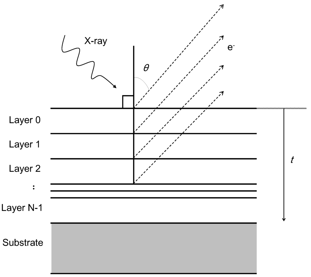
Figure 1.
A schematic picture of a layer structure. The t and e− mean the distance from the surface and photoelectrons emitted by X-ray absorption.
2.1.3. Approach for TSC
TSC observes the emission of carriers captured by traps located inside thin films or near interfaces, and provides trap density-energy level distribution Nt(Et). In TSC experiments, traps are filled with carriers and then the sample is heated at a constant rate. When the thermal energy becomes equal to the trap energy level (Et), the trapped carriers are emitted and the external current is observed. The trap density (Nt) and Et correspond to the current peak intensity and peak temperature. When a TSC peak originates from the trap with single Et, it can be easily analyzed by using a curve fitting procedure, while a peak composed of traps with several distributed Et is difficult to analyze without any assumptions regarding the number and/or distribution of Et. In this case, the model-free MEM is very useful. The basic TSC equation is [22,23]
where q, ν, k, and β are the elemental charge, the attempt-to-frequency, the Boltzmann constant, and the heating rate, i.e., the absolute temperature T of a sample is T0 + β × time. The aim of TSC is to determine Nt(Et). Equation (16) has the same shape as Equation (1); however, Nt(Et) is not a probability density function and does not satisfy Equation (2). In order to overcome this difficulty, ITSC(T) and Nt(Et) must be normalized with the normalized constant P as the next equations [22,23]
and
Usually, P cannot be determined because P is the integrated value of the MEM calculation result. However, P in TSC can be easily obtained prior to the MEM calculations because P in Equation (18) is equal to the amount of all trapped carriers as
This makes it easy to apply MEM to TSC. The basic MEM equations can be expressed as
and
Once Nt(Et)′ is determined, Nt(Et) can be obtained using P. These are the equations required for applying MEM to TSC.
2.1.4. Approach for IA
As described above, TSC can determine trap density and energy, Nt(Et). However, the energy region that TSC can measure is limited by the equipment. The conventional TSC can detect only bulk traps with Et below ≈ 1.5 eV (this corresponds to 350 °C) and cannot investigate the interface states (Dit) located at the interface between a gate insulator and underlying substrate [22,23]. The IA technique can be used to overcome these difficulties though it is easy and simple, and requires no complex equipment or measurement system. In usual IA experiments, annealing for a constant period (δt) and data measurements are repeated as shown in Figure 2.
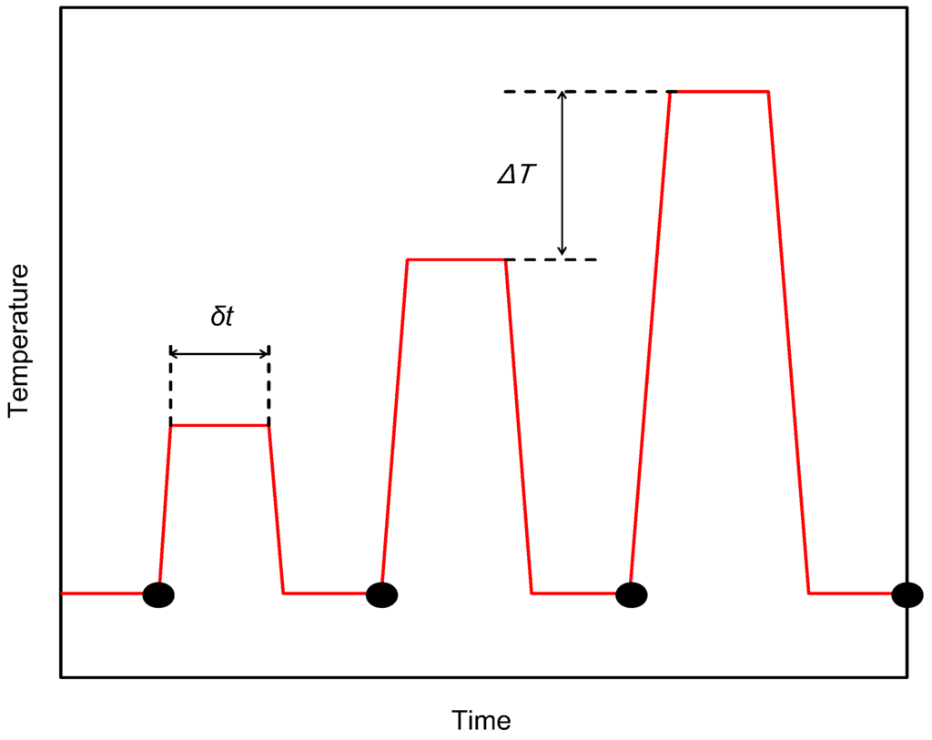
Figure 2.
A standard annealing temperature and measurement scheme used for IA experiments. The lines and circles mean sample temperature and measurement points. The ΔT and δt correspond to the temperature step and annealing period at each temperature.
In the present study, the data corresponds to annealing temperature (T) dependent midgap voltage shift ΔVmg(T) reflecting the amount of bulk trapped carriers, or to the T dependent interface state amount ΔDit(T) (note that under the midgap voltage condition, the contribution of interface states to ΔVmg is minimized; however, it cannot be completely neglected). With increasing T, ΔVmg(T) and ΔDit(T) decrease because of the emission of trapped carriers and the recovery of interface states. I explain ΔVmg(T) below; however, ΔDit(T) can be treated in the same way. The aim of IA experiments is to determine the emission (recovery for interface state cases) activation energy distribution of all traps dominating ΔVmg, i.e., ΔVmgi(Ea). Note that Ea becomes equal to Et in trap cases. The emission probability at temperature T, ep(Ea, T), is
From this, the equation
is obtained, where ΔVmg(Ea, t, Tn) means ΔVmg from trap with Ea during IA at Tn for t. This leads to
From this, the basic IA equation can be obtained [25] as
As in the TSC case, ΔVmgi(Ea) can be normalized as
where is the initial ΔVmg just after the trapping event and is directly determined by experiments. The equation
is obtained, which leads to
and
These are the equations for applying MEM to IA.
2.1.5. Approach for TDCV
This case is more problematic than the above cases because the normalization constant cannot be determined before performing the MEM calculations, and another approach is required. Let us assume a metal/SiO2/Si system for the example below. The aim of TDCV is to determine the spatial distribution of fixed charges in SiO2. First, the initial SiO2 thickness is divided into small pieces with thickness k. When the thickness is thinned to be t, e.g., by using the wet etching method, t/k is the number of involved pieces (Figure 3).
When the number n (n = 1, 2, …, t/k) is introduced, the midgap voltage shift due to fixed charges ΔVmg(t) can be calculated using the distance from the SiO2/Si interface, x:
Here, ρ(x) and P are defined by the equation
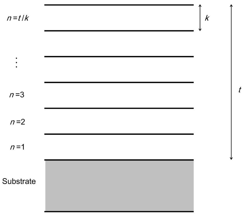
Figure 3.
A schematic picture of a layer structure. The k and t mean the thickness of each layer and the whole film thickness.
Through the use of a default function m(kn)′, the entropy term S is expressed by the equations
and
In addition, the χ2/N term is introduced:
The ρ(kn)′ that satisfies the next equation is the most probable ρ(kn)′.
Here, λ is the Lagrange parameter. Solving Equation (37), one obtains ρ(kn) as
Since this equation cannot be solved analytically, the next approximation is applied.
Equation (38) can be rewritten as Equation (40):
The ρ(kn) value can be calculated with the given m(kn) and Equation (40). If the obtained χ2/N is larger than 1, ρ(kn) is set to be a new m(kn). Repeating this calculation until χ2/N ≤ 1, one can obtain the most probable ρ(kn), i.e., ρ(x).
2.2. Numerical Calculation
This section details MEM numerical calculation results. Particular attention is paid to the number of measured data points and noise because they are very important elements for experiments. In addition, as described above, the assumed default function, m, might affect the results and thus has to be considered. The computing time also largely depends on m and the users might need to choose the appropriate m before performing the MEM calculations. Therefore, m was also examined.
2.2.1. ARXPS Case
The assumed structure for ARXPS calculation is SiO2 film on Si substrate, and C and N are distributed inside the film shown in Figure 4a. λ for C, N, Si and O are 3.37, 3.15, 3.80 and 2.80 Å [27], and Al Kα X-ray source was assumed. Generally, thin film thickness in semiconductor engineering is known in advance or can be easily determined by using spectroscopic ellipsometry, X-ray reflectivity, or XPS methods, and the Si concentration of the substrate is 100%. In this case, it is enough to perform MEM calculations under the assumption that the depth beyond the film thickness is uniform, Si = 100%, which reduces the computing time. Therefore, the composition in the region deeper than 5 nm from the surface was fixed to be Si 100%. Note that even when this assumption is not used, the obtained results are coincident within a few percent (figures not shown), though the computing time significantly varies.
First, mA(t) (A = O, Si, N, and C) dependence was examined. The ARXPS signal intensities calculated as a function of θ (0, 10, 20, ..., and 70°; total = 8 points) without noises are shown in Figure 4b. The MEM calculations were performed for two sets of mA(t) where mA(t) is set to be atomic percent determined from the intensity ratio at θ = 0°, i.e., C, N, Si, and O = 1%, 3%, 57%, and 39%, and mA(t) for all elements is equal and uniform, that is, 0.25. The MEM calculations reproduce well the calculated ARXPS intensities and the assumed depth distributions as shown in Figure 4(b)–(d). In this study little mA(t) dependence is present, but it might appear when using other calculation routines and/or the assumed depth distribution. It may also be observed if a significantly different mA(t) is used. To confirm this, I carried out the MEM calculations for different assumed atom distribution systems with various mA(t), but only negligible dependence was observed. From these results, I think that mA(t) is to a considerable extent arbitrary. On the other hand, the computing time significantly depends on mA(t), and mA(t) determined by the values at θ = 0° led to the shortest computing time in mA(t) that was tried. I therefore used the values below. If structural data determined by using methods such as Rutherford backscattering is available, one can use it as mA(t), i.e., prior knowledge, leading to more precise and faster determination.
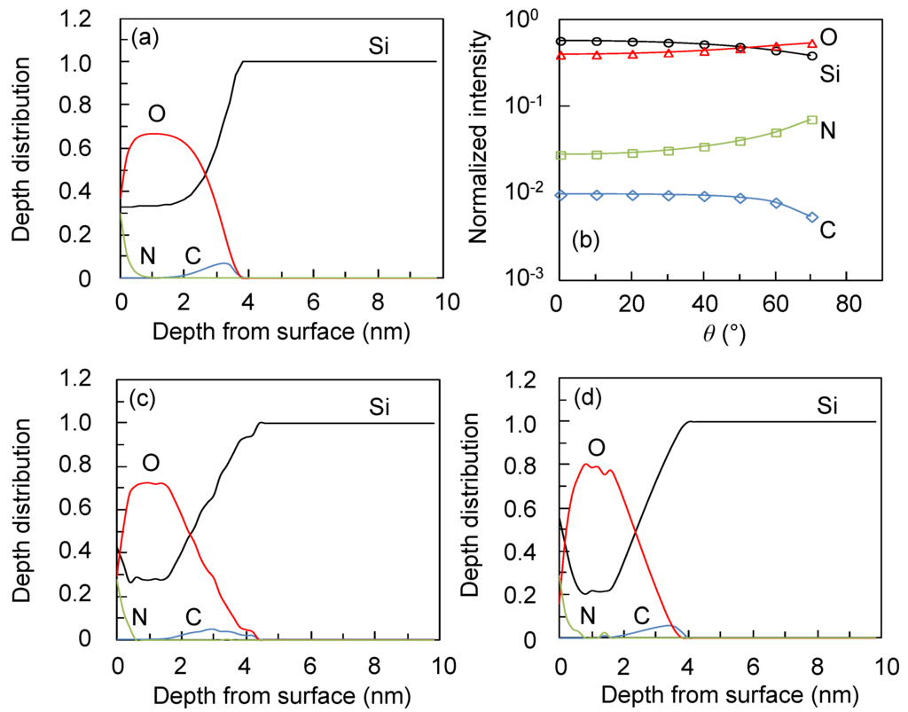
Figure 4.
The mA(t) dependence of the MEM calculation results for ARXPS (θ = 0, 10, 20, …, 70° and the no noise case). (a): Assumed depth distribution of C, N, Si, and O atoms for ARXPS-MEM calculations. (b): Normalized ARXPS intensity as a function of θ calculated from Equations (11), (12), and the depth distribution shown in (a) (symbols). The lines are the MEM calculation results with mA(t) determined by θ = 0° values. (c) and (d): Reconstructed depth distribution from ARXPS normalized intensity (symbols in (b)) using MEM with mA(t) determined respectively by θ = 0° values (c) and mA(t) = 0.25 (d) for all atoms.
Figure 5 shows the effect of the number of data points, i.e., 5, 8, or 15 points (θ = 0, 17, 34, 51, 68° for 5 points, θ = 0, 10, 20, …, 70° for 8 points, and θ = 0, 5, 10, …, 70° for 15 points). Intuitively, it would appear that more data points gives more precise results, i.e., MEM can reproduce the assumed distribution better. However, the dependence on the number of data points is insignificant. Even with only five data points, the MEM results reproduce the assumed distribution relatively well. I think that measuring the data points at eight angles is sufficient in general cases. Livesey et al. pointed out that the data measured at angles above 70° has negligible impact on the MEM calculations [16]. They also pointed out that the absolute ARXPS signal intensity becomes considerably weaker at such angles. Therefore, in many cases it is sufficient to measure the eight data points at angles under 70°. Next, the MEM tolerance to noise was examined. The MEM calculation results with ARXPS signals including artificial Gaussian noise (0%, 5%, 10%) are shown in Figure 6. It should be noted that even in the 10% case, the overall shapes of the assumed distribution are reproduced though they become somewhat distorted. This proves the validity of MEM and is very helpful for practical use.
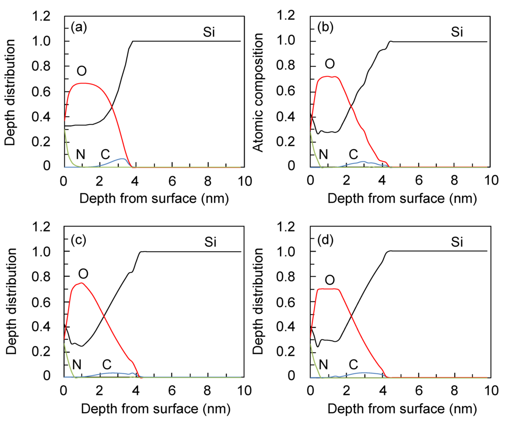
Figure 5.
Dependence of the MEM calculation results on the number of data points for ARXPS (mA(t) determined by θ = 0° values, and the no noise case). (a): Assumed depth distribution of C, N, Si, and O atoms for ARXPS-MEM calculations. (b)–(d): Reconstructed depth distribution from ARXPS normalized intensity using MEM respectively for θ = 0, 10, 20, …, 70° (8 points), θ = 0, 17, 34, 51, 68° (5 points), and θ = 0, 5, 10, …, 70° (15 points) cases.
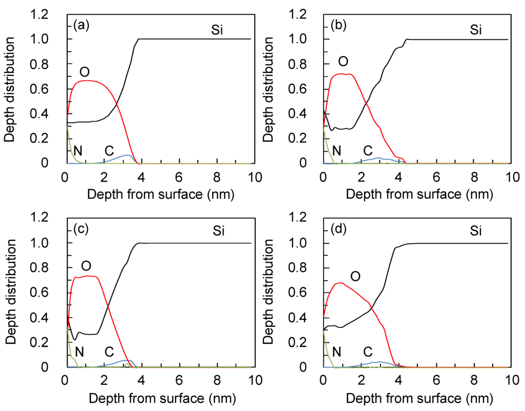
Figure 6.
Noise dependence of the MEM calculation results for ARXPS (θ = 0, 10, 20, …, 70° and mA(t) determined by θ = 0° values case). (a): Assumed depth distribution of C, N, Si, and O atoms for ARXPS-MEM calculations. (b)–(d): Reconstructed depth distribution from ARXPS normalized intensity respectively using MEM for artificially introduced Gaussian noise = 0%, 5%, and 10% cases.
2.2.2. TSC Case
For this case β = 20 K/min and ν = 1011 /s were assumed [22,23,24]. The assumed Nt(Et) distribution is shown in Figure 7a (peaks A, B, and C). The corresponding TSC spectra calculated with Equation (16) is plotted in Figure 7b. The MEM calculation results are plotted in Figure 7a,b. Constant m(Et) was used in this calculation. The MEM results well reproduce the assumed Nt(Et) distribution, which demonstrates that MEM can be applied to arbitrary Et distribution. The MEM calculations were also performed with exponential or Gaussian m(Et) and almost the same results were obtained [24]. However, the computing time significantly depended on m(Et). It becomes shorter when m(Et) is closer to the assumed Nt(Et). Thus, for practical use, one should chose m(Et) carefully. Fortunately, the appropriate m(Et) can be obtained from the equations [28]
and
These equations give Nt(Et) shown in Figure 7a. They cannot reproduce all the peaks because they directly convert to Nt(Et) and the obtained Nt(Et) trails . The broad peak C is reproduced very well but the A and B peaks are not. From this, one can conclude that although Equations (41) and (42) are easy to use, they reproduce only widely distributed . However, this can be used as m(Et) to reduce the computing time.
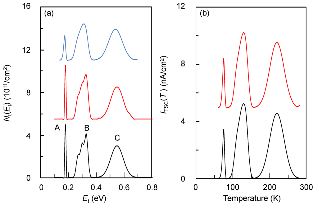
Figure 7.
Assumed Nt(Et), and MEM results. (a): From bottom to top, assumed Nt(Et), MEM reconstructed results, and Nt(Et) calculated from Equations (41), (42) and . (b): calculated from assumed Nt(Et) (lower) and MEM result (upper). MEM was performed without noise and with constant m(Et).
The number of data points in TSC spectra is usually enough, typically more than 1000, and one does not need to be concerned about this point for MEM calculations.
Regarding noise, the MEM calculation is slightly affected by noises in ITSC(T). The MEM calculation results with artificial Gaussian noises are shown in Figure 8. For larger noise, the peaks become gradually distorted. Moreover, a ghost shoulder and peak (indicated by arrows) appear. However, their effect is very slight. Note that this is an extreme case and that the usual ITSC(T) is not so noisy (see [22,23]) except for the region where ITSC(T) is extremely low (in the order of 10−15 A). Therefore, in practical use, it is thought that the noise has much less impact on the MEM calculation.
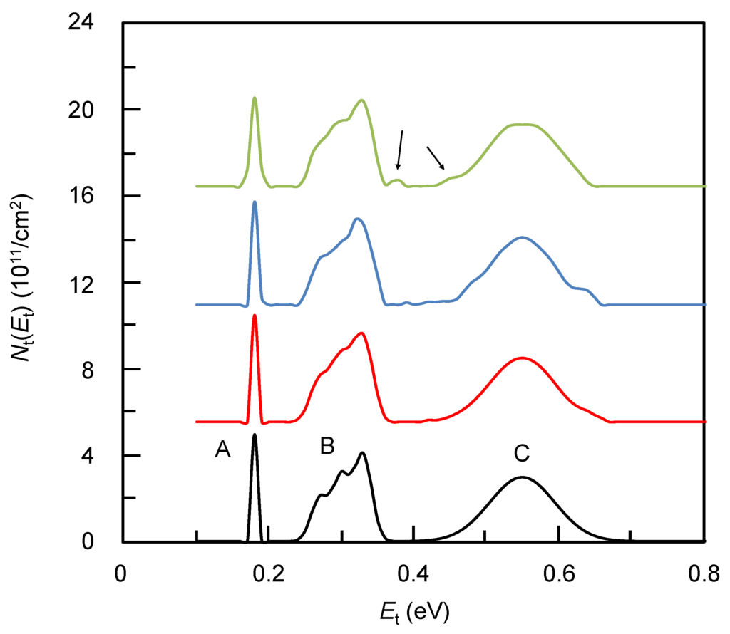
Figure 8.
Noise dependence of the MEM calculation results for TSC (constant m(Et) case). From bottom to top, assumed Nt(Et), MEM results for artificially introduced Gaussian noise = 0%, 5%, and 10% cases. The arrows indicate a ghost shoulder and peak.
2.2.3. IA Case
For this case, the ΔVmgi(Et) distribution shown in Figure 9a and ν = 1011 /s were assumed [22,23,24]. From this distribution, the corresponding ΔVmg(T) values were calculated as shown in Figure 9b. Here the calculations were performed with ΔT = 20 K and δt = 600 s. The MEM calculation results obtained with constant m(Ea) are shown in Figure 9a,b. Exponential or Gaussian m(Ea) were examined with respect to m(Ea) dependence. However, the obtained results remain almost unchanged, which means that the MEM calculations are hardly affected by the assumed m(Ea). Unfortunately, unlike the TSC case, no appropriate m(Ea) is obtainable prior to the MEM calculations and it is difficult to even predict the ΔVmgi(Ea) curves from experimental data, ΔVmg(T). Therefore, it was considered that there was no choice but to use the constant m(Ea) although the computing time might be longer than the case where the appropriate m(Ea) (closer to the ΔVmgi(Et)) is used.
With respect to the obtained ΔVmgi(Et) shown in Figure 9a, the overall shape is reproduced but there is a large deviation between the assumed distribution and the MEM results. The intensity ratio between peaks is different and the peaks are smoothed, especially peaks A and B. This is because ΔT is somewhat large and the fine structures are not reflected in ΔVmg(T) sufficiently. The ΔT value is limited by the temperature control precision of the annealing furnace. As a result, the number of data points is limited and the information in ΔVmg(T) is averaged in comparison with the above TSC case, which degrades the precision of the MEM result. Actually, when more (less) data points, i.e., ΔT is 10 K (30 K), are assumed, the reproducibility is slightly improved (degraded) as shown in Figure 9(c). Therefore, the number of data points has to be taken into consideration when MEM is used. It should be noted that although its accuracy is lower than that of TSC, IA has three distinct advantages, i.e., it can be applied to devices, can observe very deep traps while TSC can detect only traps with Et up to ≈ 1.5 eV, and can determine Diti(Ea).
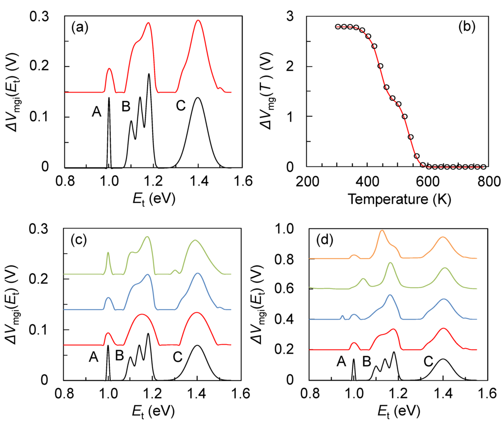
Figure 9.
The dependence of the MEM calculation results on the number of points (i.e., ΔT) and noise for the IA (constant m(Ea) case). (a): Assumed ΔVmgi(Et) (lower) and the MEM results with ΔT = 20 K and without noise (upper). (b): Calculated ΔVmg(T) from Equation (26) and (a) with ΔT = 20 K and without noise (symbol). The line corresponds to the MEM result. (c): From bottom to top, assumed ΔVmgi(Et), the MEM results without noise and with ΔT = 30, 20, and 10 K, respectively. (d): From bottom to top, assumed ΔVmgi(Et), the MEM results with ΔT = 20 K and with artificially introduced Gaussian noise = 0%, 5%, 8%, and 10%, respectively.
Regarding noise, I examined the noise dependent MEM calculations and the results are shown in Figure 9d. The noise significantly affects the obtained spectra, especially on peak A. This peak is very sharp and its recovery occurs in a very narrow temperature range, i.e., ΔVmg(T) drops very sharply with temperature. As a result, the drop is included in only a few data points and it is susceptible to noise. This even shifts the peak A position. Similarly, peak B is considerably distorted. Meanwhile, the broad peak C is less susceptible to noise as expected from the above argument. This means that one should obtain high signal-to-noise ratio data for the MEM calculations.
2.2.4. TDCV Case
I assumed a SiO2(10 nm)/Si system with the three fixed charge distributions, ρ(t), shown in Figure 10a–c. The ΔVmg(t) calculated from each ρ(t) and the corresponding MEM results are plotted in Figure 10(a)–(d). The m(kn) value is impossible to deduce before MEM calculation. If ρ(t) is proportional to thickness, the distribution is localized at the interface. On the other hand, the distribution is uniform inside a film when ρ(t)2 is proportional to the thickness. From these, one can deduce m(kn); however, this estimation is insufficient in many cases. Therefore, a constant m(kn) value was assumed although the computing time might be longer. Since this assumption seems to work well (see the results for the 10 point case), one can conclude that the constant m(kn) can be used when deducing its value is difficult.
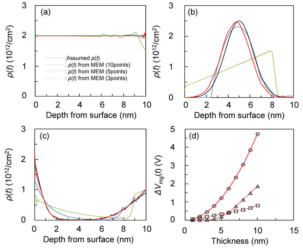
Figure 10.
Assumed fixed charge distribution and the number of points dependence of the MEM calculation results for TDCV (constant m(kn) and the no noise case). (a)–(c): The black lines are the assumed rho(t). The colored lines are the MEM calculated results with the number of points = 10, 5, and 3. (d): The circles, triangles, and squares are calculated ΔVmg(t) for the assumed distribution rho(t) in (a)–(c), respectively. The lines are the corresponding MEM calculation results.
In addition, the number of the corresponding ΔVmg(t) data points are set to be 10, 5, and 3 to confirm the dependence of the MEM calculation accuracy on the number of data points. The obtained MEM results are plotted in Figure 10a–c. It would intuitively seem that fewer data points would result in less accurate results, as expected from the IA case. This was found to be the case; the MEM results significantly depend on the number of data points. When it is 10, MEM reproduces the assumed distributions well, while a slight (significant) deviation is seen for the 5 (3) point case. Therefore, one can conclude that at when MEM is applied to TDCV, at least 10 points are required to obtain satisfactory results.
Noise was found to have a considerable impact on the MEM calculation results (Figure 11). In particular, a large deviation from the assumed ρ(t) appears when the noise exceeds 5%. The peak becomes distorted and even a ghost shoulder and peak are present in the 10% case. However, one does not need to take noise into consideration since in general cases the CV measurement accuracy is less than 5%.
In concluding this section, I can state that MEM can analyze the data accurately without any prior knowledge regarding the results. In the next section, I will explain an example of application results to assist readers’ understanding of the validity of MEM.
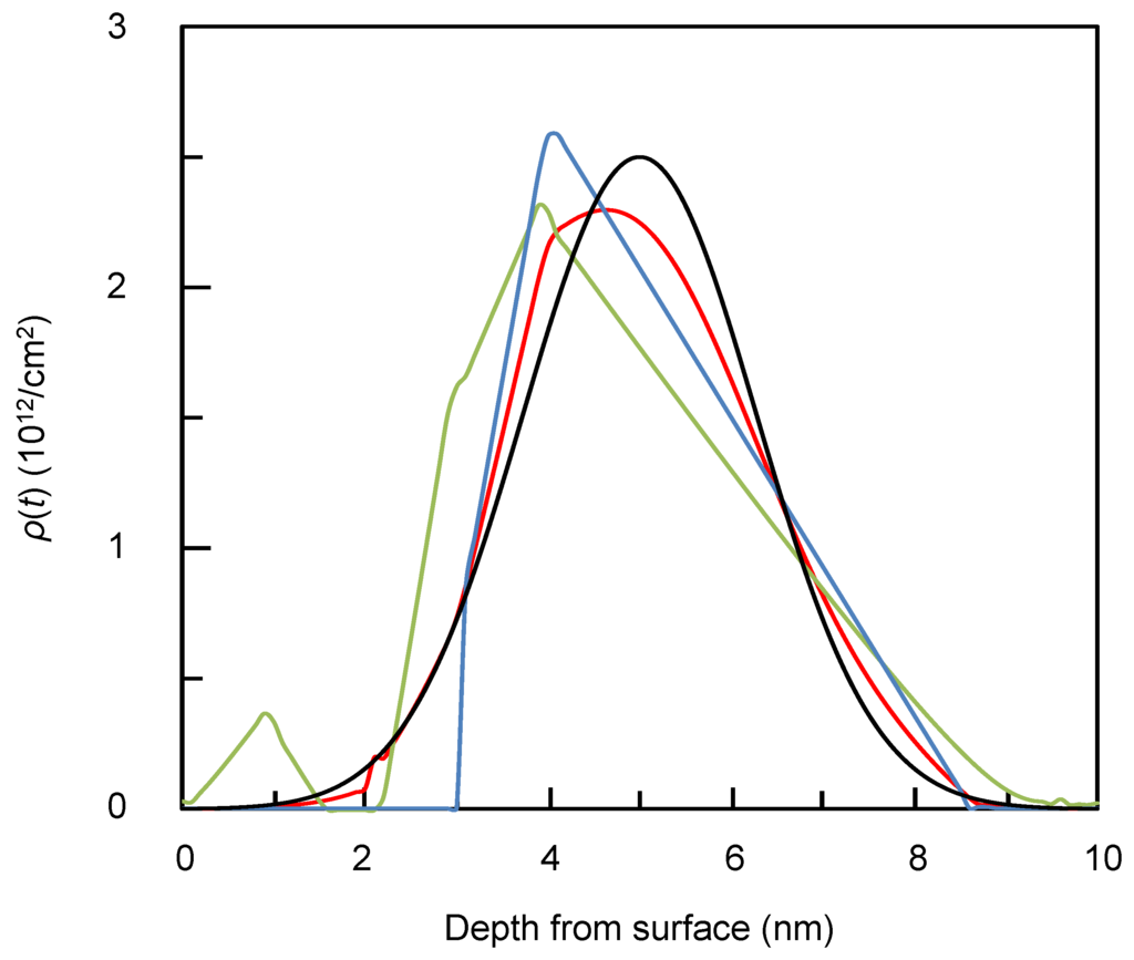
Figure 11.
Noise dependence of the MEM calculation results for TDCV (constant m(kn) and the 10 point case). The black line is the assumed ρ(t). The red, blue, and green lines correspond to the artificially introduced Gaussian noise = 3%, 5%, and 10% cases, respectively.
3. Experiments and MEM Calculations
For experiments, SiO2/Si wafers contaminated with carbon were prepared. Cleaned Si(100) wafers were left in air for tl = 0, 1, 3, or 10 weeks, during which carbon contaminations adsorbed onto the wafers. Then, the wafers were cut into small pieces (1 × 1 cm2) and annealed in O2 ambient at 1100 °C until 10 nm thermal SiO2 was grown. For ARXPS, SiO2 was thinned to be 4 nm (thickness was monitored with a spectroscopic ellipsometer). ARXPS spectra for C 1s, O 1s, and Si 2p were measured with θ = 0, 10, 20, …, 70°. Monochromatized Al Kα was the X-ray source. Before measurements, the sample surfaces were cleaned with H2SO4 + H2O2 solvent to remove surface carbon adsorbates. Integrated peak intensity depending on θ was determined by peak fitting using a Gaussian function after subtracting the Shirley background. For the MEM calculations, mA(t) were determined from the measurement results at θ = 0°. For λC, λSi, and λO, 3.37, 3.80, and 2.80 Å were used, respectively [27].
For TSC measurement, all the contaminated 10 nm SiO2 films were cleaned with H2SO4 + H2O2 solvent. Immediately following the cleaning, aluminum (99.99 % purity) electrodes with diameter 300 μ m were deposited onto the sample surface by vacuum evaporation technique (metal oxide semiconductor (MOS) structure). In addition, gold back contact electrodes were fabricated. The MOS mounted onto the sample holder specified for TSC was inserted into a chamber, the atmosphere in which was replaced with pure He gas. The avalanche injection technique was used to selectively inject holes into SiO2. The MOS temperature was then increased up to 350 °C with constant heating rate β = 20 K/min. During the heating up, the external current due to the emission of trapped holes was detected as the TSC signal ITSC(T). The current sensitivity was ≈ 5 × 10⁻¹⁵ A. For the MEM calculations that were performed, ν was assumed to be 1011 /s [22,23,24]. Although for precisely determining the absolute value of Et, ν must be determined by other methods [24,29], it is sufficient for our purpose to distinguish Et because Nt(Et) merely shifts by about 0.1 eV toward higher Et for ν larger by one order [24]. The m(Et) value was calculated from ITSC(T), Equations (41) and (42).
For IA measurements, the same samples as those for the TSC case were used. After avalanche injection, IA was performed following the temperature and ΔVmg(T) (ΔDit(T)) measurement sequence shown in Figure 12. For T≤300 K, the values were measured at T, while the measurements were performed at 300 K for T≥300 K to avoid damage that might be imposed by high temperature measurements. The IA temperature step ΔT and period δt were set to be 20 K and 600 s. The heating rate was 20 K/min. All the IA measurements were carried out under N2 ambient. The ΔVmg(T) (ΔDit(T)) values were recorded using an LCR meter. This ΔVmg(T) data includes the contributions of the trapped charges and interface states (although the latter are minimized at midgap voltage, a few of them can be included), while ΔDit(T) is determined only by the interface state density. For ν and m(Ea) for MEM calculations, 1011/s [22,23,24] and the constant m(Ea) were used. In order to reduce experimental noise, the same measurements were repeated four times and the data were averaged.
The same contaminated samples were also used for TDCV measurements. An HF solution was used to thin SiO2 to several thickness t. Then, MOS capacitor structures were formed. The Vmg(t) for each sample was recorded with an LCR meter. The ΔVmg(t) was determined from the differences of Vmg(t) between non-contaminated and contaminated samples. All the measurements were performed at room temperature. A constant m(kn) was used for MEM calculations.
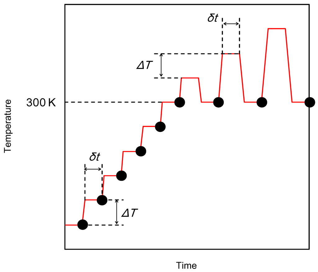
Figure 12.
The IA temperature and measurement scheme for contaminated MOS samples.
4. Results and Discussion
The MEM calculation results on ARXPS are shown in Figure 13 (only C depth distribution is shown). Clearly, the depth distributions depend on tl. Most carbon is located near the interface, while the amount of carbon atoms increases for longer tl. These carbon atoms are undoubtedly due to the carbon contamination. Note that C present near the surface is due to the surface C adsorbates and is not discussed in this paper.
In TSC in Figure 14a, the peaks A and C decrease for longer tl. In addition, new B peaks are observed in longer tl samples, which implies the carbon contamination generates new traps. The TSC peaks are too broad to analyze using a cure fitting method. The MEM calculation results are shown in Figure 14a,b. Several peaks can be clearly observed at around 0.8, 1.1, and 1.3 eV. The tl = 0 sample without the carbon contamination shows no 1.1 eV peak, while 0.8 and 1.3 eV peaks are clearly present, which indicates that the 1.1 eV peak originates from the carbon, while the others are intrinsic SiO2 traps. From [30,31], the A and C peaks can be - and -centers (oxygen deficiency), respectively. This A and C peak intensity becomes less for longer tl, which implies that the oxygen deficiencies are passivated by the carbon. Therefore, the dependence of A and C peaks on the carbon is different from that of B. In addition, for tl ≥ 1 week samples, the B peak appears at almost the same Et. This may mean that the chemical bonding state around the carbon atoms is independent of tl although its detailed atomic bonding structure cannot be determined.
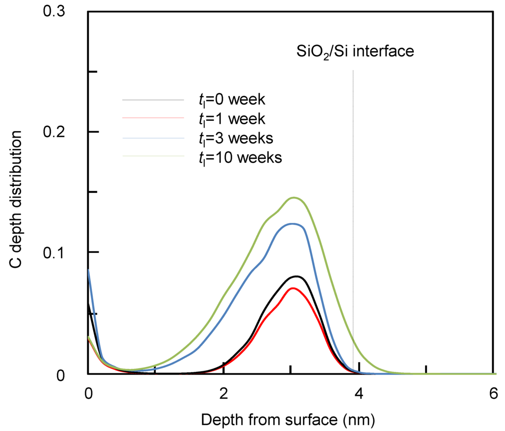
Figure 13.
The tl dependence of carbon distribution in contaminated MOS samples determined from ARXPS and MEM calculations.
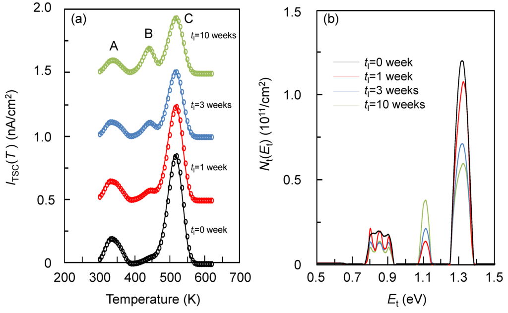
Figure 14.
The tl dependence of ITSC(T) for contaminated MOS samples (a) and Nt(Et) calculated with MEM (b).
As described above, although TSC provides unique information regarding Nt and Et, it can detect traps only up to 1.5 eV. This problem can be overcome using the IA technique. The ΔVmg(T) plot in Figure 15a shows that ΔVmg(T) begins to decrease at around 300 K. Since this temperature is close to that at which the lowest TSC energy peak appears, this decrease may originate from the emission of holes from the same trap (A peak in TSC). In addition, ΔVmg(T) shapes depend on tl. However, it is difficult to interpret this dependence, although it implies additional detrapping and/or the recovery of interface states. The ΔVmg(T) are settled at almost 0 after 700 K IA. This results from the complete detrapping and/or the recovery of interface states. In other words, all the Ea of traps and/or interface states can be detected by the IA technique.
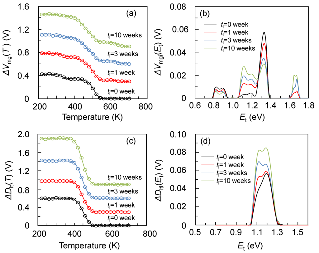
Figure 15.
The tl dependence of ΔVmg(T) (a) and ΔDit(T) (c) in contaminated MOS samples. The ΔVmgi(Ea) (b) and ΔDiti(Ea) (d) are the corresponding MEM calculation results.
The MEM results are shown in Figure 15b. It should be remarked that some peaks were clearly extracted. In comparison with the TSC peaks in Figure 14, 0.8, 1.1, and 1.3 eV peaks can be attributed to the detrapping of holes captured during the avalanche stresses. Therefore, the other peaks at 1.2 and 1.7 eV originate from other traps or the recovery of interface states. For more detailed investigation, ΔDit(T) was analyzed and the results are shown in Figure 15c,d. Note that although ΔDiti(Ea) is the interface state density and its unit is /cm2, we use the unit V to make the comparison with ΔVmgi(Ea) (in unit V) easier. In the obtained ΔDiti(Ea), some peaks are observed at around 1.2 eV. Therefore, the 1.2 eV peak in Figure 15b corresponds to the recovery of the interface states formed by the avalanche stresses. On the other hand, the fact that no ΔDiti(Ea) peaks appear at 1.7 eV suggests that the 1.7 eV peak can be attributed to a hole trap that could not be observed by TSC. Both the 1.2 and 1.7 eV peaks increase for longer tl, which indicates that the carbon contamination accelerates the formation of interface states and hole traps.
The TDCV experiment results are described next. Figure 16a shows TDCV curves. It should be noted that for longer tl, ΔVmg(t) is larger. This indicates that more carbon contamination yields more fixed charges. The ΔVmg(t) value decreases as the films are thinned; however, it is difficult to extract the distribution of the fixed charges in these films from the curves.
Figure 16b shows the MEM results. As shown in ΔVmg(t), the amount of fixed charges increases considerably with more carbon contamination, i.e., for longer tl. This indicates that carbon produces fixed charges. The distribution ρ(t) decreases toward bulk, which implies that carbon diffused into SiO2 during oxidation.
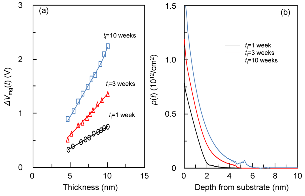
Figure 16.
The tl dependence of ΔVmg(t) for contaminated MOS samples (a) and ρ(t) calculated with MEM (b).
These four experiments and MEM calculations provide information that can be easily and intuitively understood. Thus, the carbon species adsorbed on the surface were incorporated diffusively into the SiO2 film during the thermal oxidation process. This diffusion results in the carbon distribution shown in Figure 13. In addition, the incorporated carbon yields new traps and simultaneously passivates the intrinsic traps, - and -center. Moreover, the carbon accelerates the formation of interface states and also forms fixed charges. Note that the distribution of the fixed charges resembles the carbon atom distribution (both are localized near the interface) although their amounts differ by many orders, which means that only a part of the incorporated carbon atoms forms fixed charges. This is the effect of carbon contamination on the structural and electrical properties of MOS capacitors. Unfortunately, this study yielded no information regarding the precise atomic structure of traps, fixed charges, and interface states. However, it is evident that MEM is a very powerful tool for semiconductor engineering and provides crucial information that cannot be extracted with conventional methods. Furthermore, MEM can be easily applied to other experimental data analysis including the inverse problems described by Equation (1). In this respect, rapid growth of MEM application to engineering fields as well as to physics and chemistry can be expected.
5. Conclusions
This paper describes a brief theoretical background and application results regarding MEM data processing from the viewpoint of the application to semiconductor engineering. The MEM method was applied to the analysis of ARXPS, TSC, IA, and TDCV data, which provided evidence that it can extract very interesting and crucial information regarding atom distribution, traps, fixed charges, and interface states. These data are of great importance for device fabrication processes and the understanding of their physics. The MEM method is very simple and can be applied easily to other data including inverse problems. It can be expected that MEM’s importance in the engineering field will continue to grow, and that the method will become a standard analyzing tool.
Acknowledgments
I would like to thank I. Yamakawa at Hitachi, Ltd. for his useful advice and comments about the application of MEM to ARXPS.
References
- Collins, D.M. Electron density images from imperfect data by iterative entropy maximization. Nature 1982, 298, 49–51. [Google Scholar] [CrossRef]
- Takata, M.; Umeda, B.; Nishibori, E.; Sakata, M.; Saitoh, Y. Confirmation by X-ray diffraction of the endohedral nature of the metallofullerene Y@C82. Nature 1995, 377, 46–49. [Google Scholar] [CrossRef]
- Takata, M.; Nishibori, E.; Umeda, B.; Sakata, M.; Yamamoto, E.; Shinohara, H. Structure of Endohedral Dimetallofullerene Sc2@C84. Phys. Rev. Lett. 1997, 78, 3330–3333. [Google Scholar] [CrossRef]
- Nishibori, E.; Ishihara, M.; Takata, M.; Sakata, M.; Ito, Y.; Inoue, T.; Shinohara, H. Bent(metal)2C2 clusters encapsuated in (Sc2C2)@C82(III) and (Y2C2)@C82(III) metallofullerenes. Chem. Phys. Lett. 2006, 433, 120–124. [Google Scholar] [CrossRef]
- Noritake, T.; Aoki, M.; Seno, Y.; Hirose, Y.; Nishibori, E.; Takata, M.; Sakata, M. Chemical bonding of hydrogen in MgH2. Appl. Phys. Lett. 2002, 81, 2008–2010. [Google Scholar] [CrossRef]
- Kitaura, R.; Kitagawa, S.; Kubota, Y.; Kobayashi, T.C.; Kindo, K.; Mita, Y.; Matsuo, A.; Kobayashi, M.; Chang, H.; Ozawa, T.C.; et al. Formation of a one-dimensional array of oxygen in a microporous metal-organic solid. Science 2002, 298, 2358–2361. [Google Scholar] [CrossRef] [PubMed]
- Nishibori, E.; Nakamura, T.; Arimoto, M.; Aoyagi, S.; Ago, H.; Miyano, M.; Ebisuzaki, T.; Sakata, M. Application of maximum-entropy maps in the accurate refinement of a putative acylphosphatase using 1.3 Åx-ray diffraction data. Acta Cryst. 2008, D64, 237–247. [Google Scholar]
- Livesey, A.K.; Brochon, J.C. Analyzing the distribution of decay constants in pulse-fluorimetry using the maximum entropy method. Biophys. J. 1987, 52, 693–706. [Google Scholar] [CrossRef]
- Boukari, H.; Long, G.G.; Harris, M.T. Polydispersity during the formation and growth of the stober silica particles from small-angle X-ray scattering measurements. J. Colloid Interface Sci. 2000, 229, 129–139. [Google Scholar] [CrossRef] [PubMed]
- Elliott, J.A.; Hanna, S.; Elliot, A.M.S.; Cooley, G.E. Interpretation of the small-angle X-ray scattering from swollen and oriented perfluorinated ionomer membranes. Macromolecules 2000, 33, 4161–4171. [Google Scholar] [CrossRef]
- Takata, M.; Sakata, M.; Kumazawa, S.; Larsen, F.K.; Iversen, B.B. A direct investigation of thermal vibrations of beryllium in real space through the maximum-entropy method applied to single-crystal neutron diffraction data. Acta Cryst. 1994, A50, 330–337. [Google Scholar] [CrossRef]
- Sakata, M.; Uno, T.; Takata, M.; Howard, C.J. Maximum-entropy-method analysis of neutron diffraction data. J. Appl. Cryst. 1993, 26, 159–165. [Google Scholar] [CrossRef]
- Potton, J.A.; Daniell, G.J.; Rainford, B.D. Particle size distributions from SANS data using the maximum entropy method. J. Appl. Cryst. 1988, 21, 663–668. [Google Scholar] [CrossRef]
- Potton, J.A.; Daniell, G.J.; Rainford, B.D. A new method for the determination of particle size distributions from small-angle neutron scattering measurements. J. Appl. Cryst. 1988, 21, 891–897. [Google Scholar] [CrossRef]
- Ueda, K. Using anomalous dispersion effect for maximum entropy method analysis of X-ray reflectivity from thin-film stacks. J. Phys. 2007, 83, 012004–012009. [Google Scholar] [CrossRef]
- Livesey, A.K.; Smith, G.C. The determination of depth profiles from angle-dependent XPS using maximum entropy data analysis. J. Electron. Spectrosc. Relat. Phenom. 1994, 67, 439–461. [Google Scholar] [CrossRef]
- Scorciapino, M.A.; Navarra, G.; Elsener, B.; Rossi, A. Nondestructive surface depth profiles from angle-resolved x-ray photoelectron spectroscopy data using the maximum entropy method. I. A new protocol. J. Phys. Chem. C 2009, 113, 21328–21337. [Google Scholar] [CrossRef]
- Iwai, H.; Hammond, J.S.; Tanuma, S. Recent status of thin film analyses by XPS. J. Surf. Anal. 2009, 15, 264–270. [Google Scholar]
- Chang, J.P.; Green, M.L.; Donnelly, V.M.; Opila, R.L.; Eng, J., Jr.; Sapjeta, J.; Siverman, P.J.; Weir, B.; Lu, H.C.; Gustafsson, T.; Garfunkel, E. Profiling nitrogen in ultrathin silicon oxynitrides with angle-resolved x-ray photoelectron spectroscopy. J. Appl. Phys. 2000, 87, 4449–4455. [Google Scholar] [CrossRef]
- Toyoda, S.; Okabayashi, J.; Oshima, M.; Liu, G.L.; Liu, Z.; Ikeda, K.; Usuda, K. Chemical-state resolved in-depth profiles of gate-stack structures on Si studied by angular-dependent photoemission spectroscopy. Surf. Interface Anal. 2008, 40, 1619–1622. [Google Scholar] [CrossRef]
- He, G.; Zhang, L.D.; Fang, Q. Silicate layer formation at HfO2/SiO2/Si interface determine by x-ray photoelectron spectroscopy and infrared spectroscopy. J. Appl. Phys. 2006, 100, 083517–083521. [Google Scholar] [CrossRef]
- Yonamoto, Y.; Inaba, U.; Akamatsu, N. Detection of nitrogen related traps in nitrided/reoxidized silicon dioxide films with thermally stimulated current and maximum entropy method. J. Appl. Phys. 2011, 98, 232906–232908. [Google Scholar] [CrossRef]
- Yonamoto, Y.; Inaba, U.; Akamatsu, N. Detailed study about influence of oxygen on trap properties in SiOxNy by the thermally stimulated current and maximum entropy method. Solid-State Electron. 2011, 64, 54–56. [Google Scholar] [CrossRef]
- Yonamoto, Y.; Akamatsu, N. New determination method of arbitrary energy distribution of traps in metal-oxide-semiconductor field effect transistor. Solid-State Electron. 2012, 75, 69–73. [Google Scholar] [CrossRef]
- Yonamoto, Y. Generation/recovery mechanism of defects responsible for the permanent component in negative bias temperature instability. J. Appl. Phys. submitted. [CrossRef]
- Von der Linden, W. Maximum-entropy data analysis. Appl. Phys. 1995, 60, 155–165. [Google Scholar] [CrossRef]
- Penn, D.R. Electron mean-free-path calculations using a model dielectric function. Phys. Rev. B 1987, 35, 482–486. [Google Scholar] [CrossRef]
- Simmons, J.G.; Taylor, G.W.; Tam, M.C. Thermally stimulated currents in semiconductors and insulators having arbitrary trap distributions. Phys. Rev. B 1973, 7, 3714–3719. [Google Scholar] [CrossRef]
- Saigné, F.; Dusseau, L.; Albert, L.; Fresquet, J.; Gasiot, J.; David, J.P.; Ecoffet, R.; Schrimpf, D.R.; Galloway, K.F. Experimental determination of the frequency factor of thermal annealing processes in meta-oxide-semiconductor gate-oxide structures. J. Appl. Phys. 1997, 82, 4102–4106. [Google Scholar] [CrossRef]
- Buscarino, G.; Agnello, S.; Gelardi, F.M. Delocalized nature of the center in amorphous silicon dioxide. Phys. Rev. Lett. 2005, 94, 125501–125504. [Google Scholar] [CrossRef] [PubMed]
- Conley, J.F., Jr.; Lenahan, P.M.; Lelis, A.J.; Oldham, T.R. Electron spin resonance evidence that centers can behave as switching oxide traps. IEEE Trans. Nucl. Sci. 1995, 42, 1744–1749. [Google Scholar] [CrossRef]
© 2013 by the author; licensee MDPI, Basel, Switzerland. This article is an open access article distributed under the terms and conditions of the Creative Commons Attribution license ( http://creativecommons.org/licenses/by/3.0/).