by
Sajid Sajid 1,2 , Salem Alzahmi 1,2,*, Dong Wei 3, Imen Ben Salem 4, Jongee Park 5 and Ihab M. Obaidat 2,6,*
, Salem Alzahmi 1,2,*, Dong Wei 3, Imen Ben Salem 4, Jongee Park 5 and Ihab M. Obaidat 2,6,*
1
Department of Chemical & Petroleum Engineering, United Arab Emirates University, Al Ain P.O. Box 15551, United Arab Emirates
2
National Water and Energy Center, United Arab Emirates University, Al Ain P.O. Box 15551, United Arab Emirates
3
College of Physics and Energy, Fujian Normal University, Fuzhou 350007, China
4
College of Natural and Health Sciences, Zayed University, Abu Dhabi P.O. Box 144534, United Arab Emirates
5
Department of Metallurgical and Materials Engineering, Atilim University, Ankara 06836, Turkey
6
Department of Physics, United Arab Emirates University, Al Ain P.O. Box 15551, United Arab Emirates
Nanomaterials 2023, 13(2), 250; https://doi.org/10.3390/nano13020250 - 6 Jan 2023
Cited by 8 | Viewed by 3038
Abstract
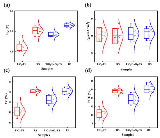
Simplifying device layout, particularly avoiding the complex fabrication steps and multiple high-temperature treatment requirements for electron-selective layers (ESLs) have made ESL-free perovskite solar cells (PSCs) attractive. However, the poor perovskite/substrate interface and inadequate quality of solution-processed perovskite thin films induce inefficient interfacial-charge extraction,
[...] Read more.
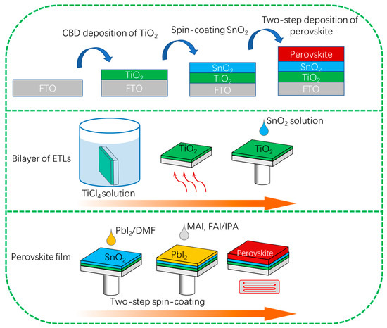
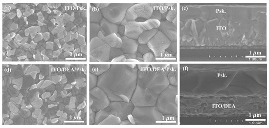
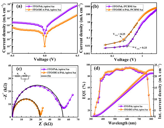
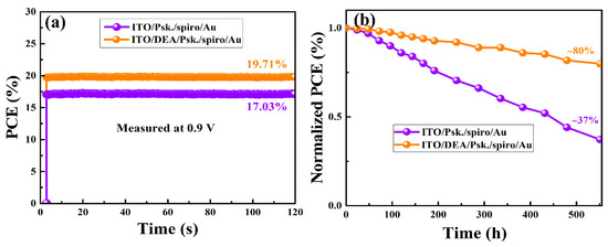
Simplifying device layout, particularly avoiding the complex fabrication steps and multiple high-temperature treatment requirements for electron-selective layers (ESLs) have made ESL-free perovskite solar cells (PSCs) attractive. However, the poor perovskite/substrate interface and inadequate quality of solution-processed perovskite thin films induce inefficient interfacial-charge extraction, limiting the power conversion efficiency (PCEs) of ESL-free PSCs. A highly compact and homogenous perovskite thin film with large grains was formed here by inserting an interfacial monolayer of diethanolamine (DEA) molecules between the perovskite and ITO substrate. In addition, the DEA created a favorable dipole layer at the interface of perovskite and ITO substrate by molecular adsorption, which suppressed charge recombination. Comparatively, PSCs based on DEA-treated ITO substrates delivered PCEs of up to 20.77%, one of the highest among ESL-free PSCs. Additionally, this technique successfully elongates the lifespan of ESL-free PSCs as 80% of the initial PCE was maintained after 550 h under AM 1.5 G irradiation at ambient temperature.
Full article
(This article belongs to the Special Issue State-of-the-Art Nanomaterials for Solar Cells)
▼
Show Figures

Graphical abstract


