Micromachines 2022, 13(6), 958; https://doi.org/10.3390/mi13060958 - 17 Jun 2022
Cited by 10 | Viewed by 2954
Abstract
The die-bonding layer between chips and substrate determinates the heat conduction efficiency of high-power LED. Sn-based solder, AuSn20 eutectic, and nano-Ag paste were widely applied to LED interconnection. In this paper, the optical–thermal performances and high-temperature reliability of LED with these bonding materials
[...] Read more.
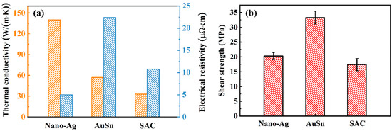
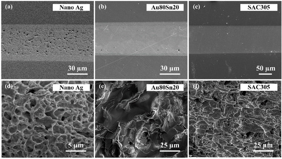
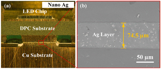
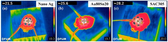
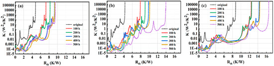
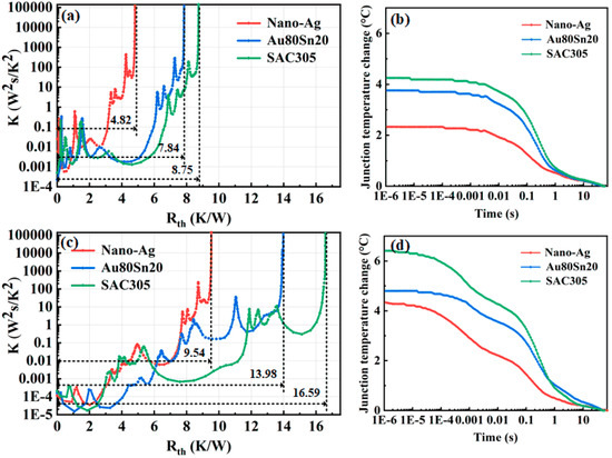
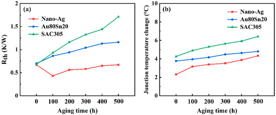
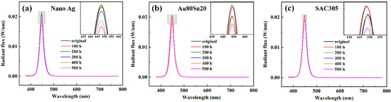
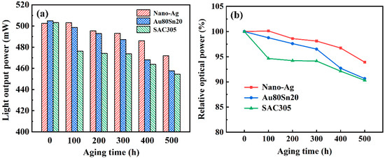
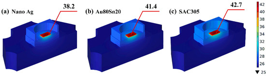
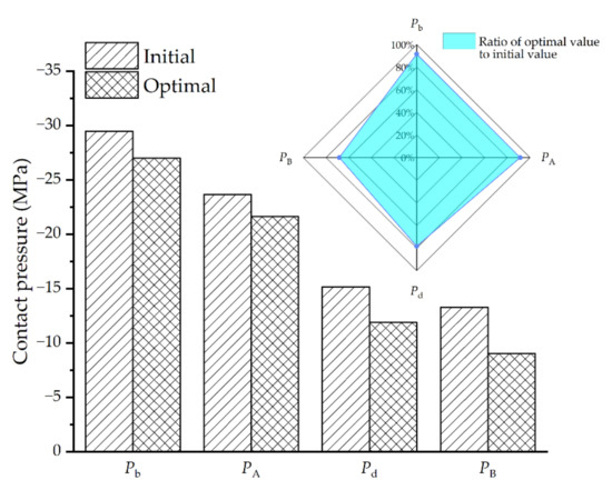
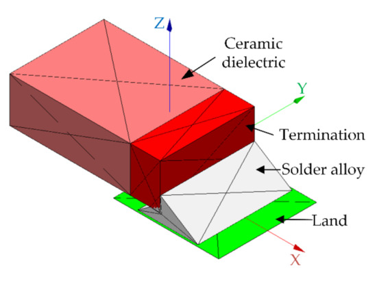
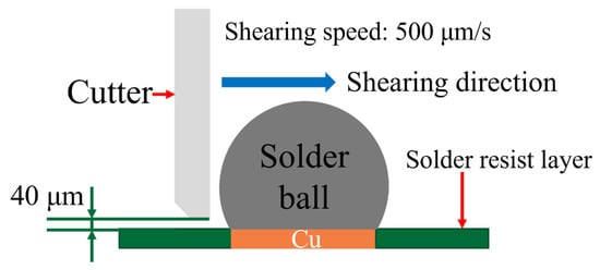
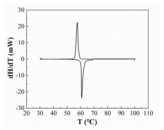
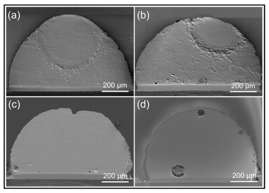
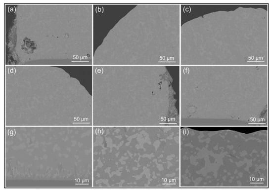
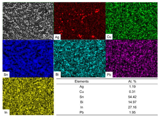
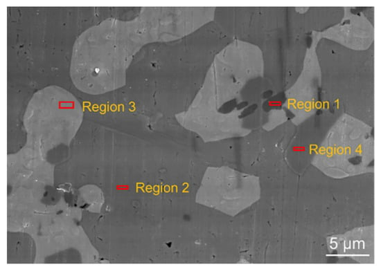
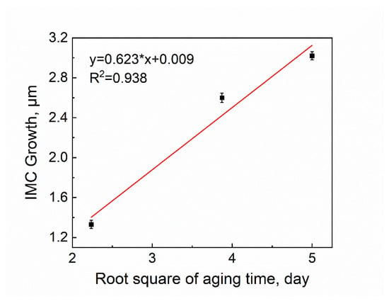
The die-bonding layer between chips and substrate determinates the heat conduction efficiency of high-power LED. Sn-based solder, AuSn20 eutectic, and nano-Ag paste were widely applied to LED interconnection. In this paper, the optical–thermal performances and high-temperature reliability of LED with these bonding materials have systematically compared and studied. The thermal conductivity, electrical resistivity, and mechanical property of these bonding materials were characterized. The LED module packaged with nano-Ag has a minimum working temperature of 21.5 °C. The total thermal resistance of LED packaged with nano-Ag, Au80Sn20, and SAC305 is 4.82, 7.84, and 8.75 K/W, respectively, which is 4.72, 6.14, and 7.84 K/W higher after aging for 500 h. Meanwhile, the junction temperature change of these LEDs increases from 2.33, 3.76, and 4.25 °C to 4.34, 4.81, and 6.41 °C after aging, respectively. The thermal resistance of the nano-Ag, Au80Sn20 and SAC305 layer after aging is 1.5%, 65.7%, and 151.5% higher than before aging, respectively. After aging, the LED bonded with nano-Ag has the better optical performances in spectral intensity and light output power, which indicates its excellent heat dissipation can improve the light efficiency. These results demonstrate the nano-Ag bonding material could enhance the optical-thermal performances and high-temperature reliability of high-power LED.
Full article
(This article belongs to the Special Issue Advanced Technologies in Electronic Packaging)
►
Show Figures
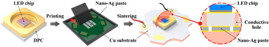
Figure 1


