
Stretchable Metamaterial Absorber Using Liquid Metal-Filled Polydimethylsiloxane (PDMS)


Abstract
:1. Introduction
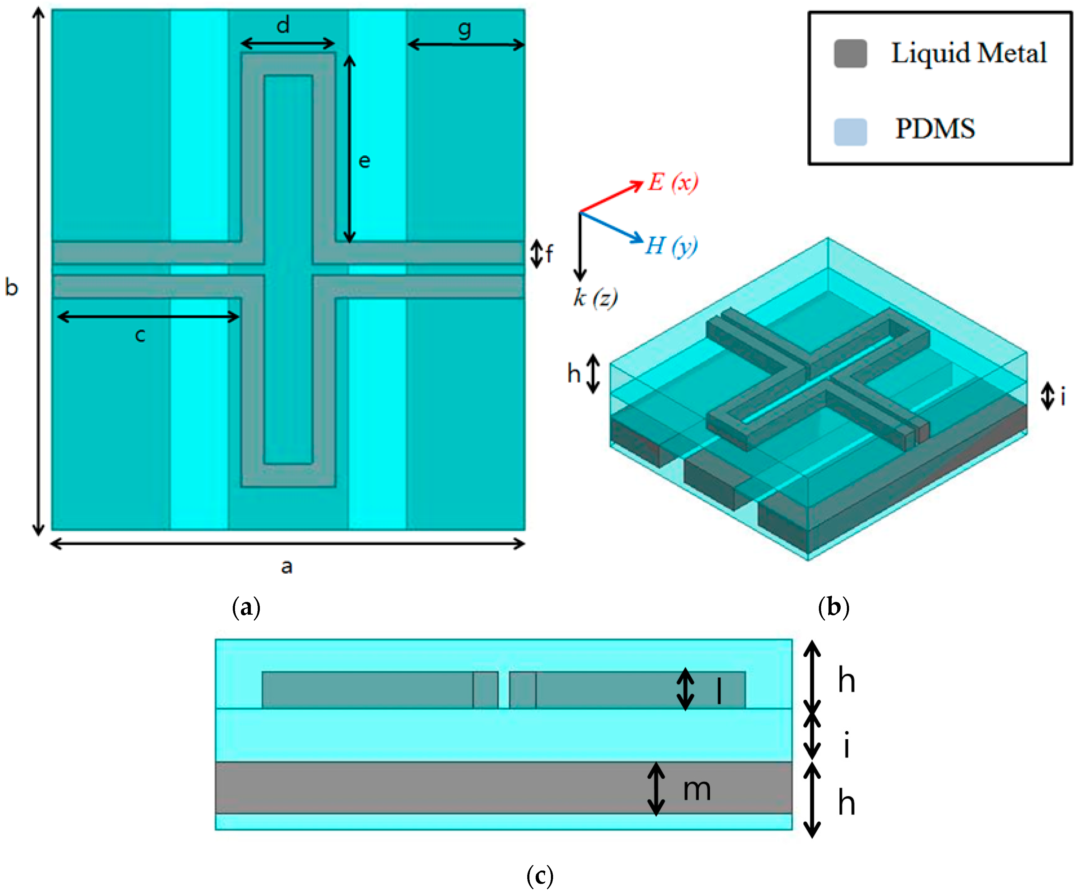
2. Design
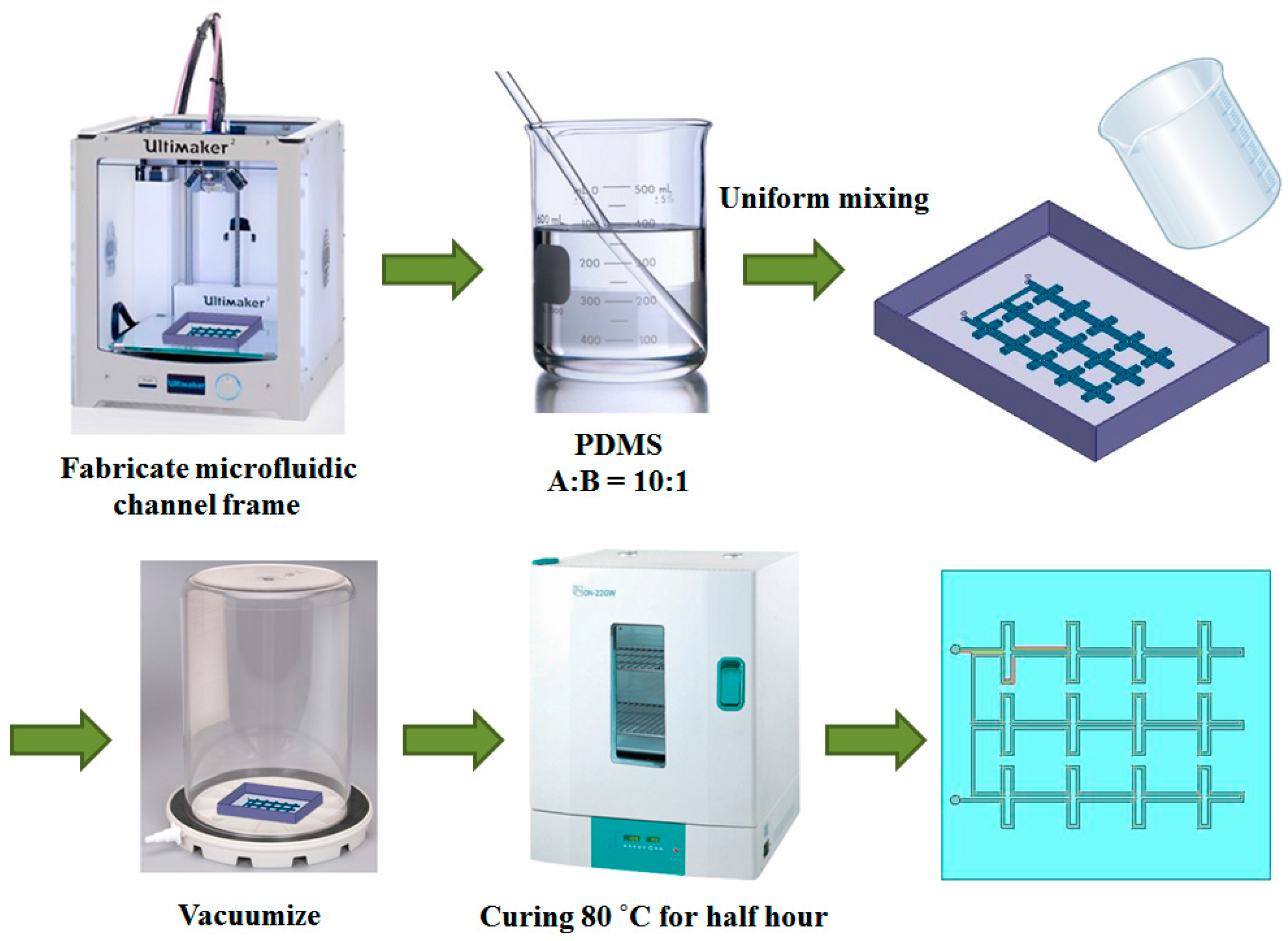
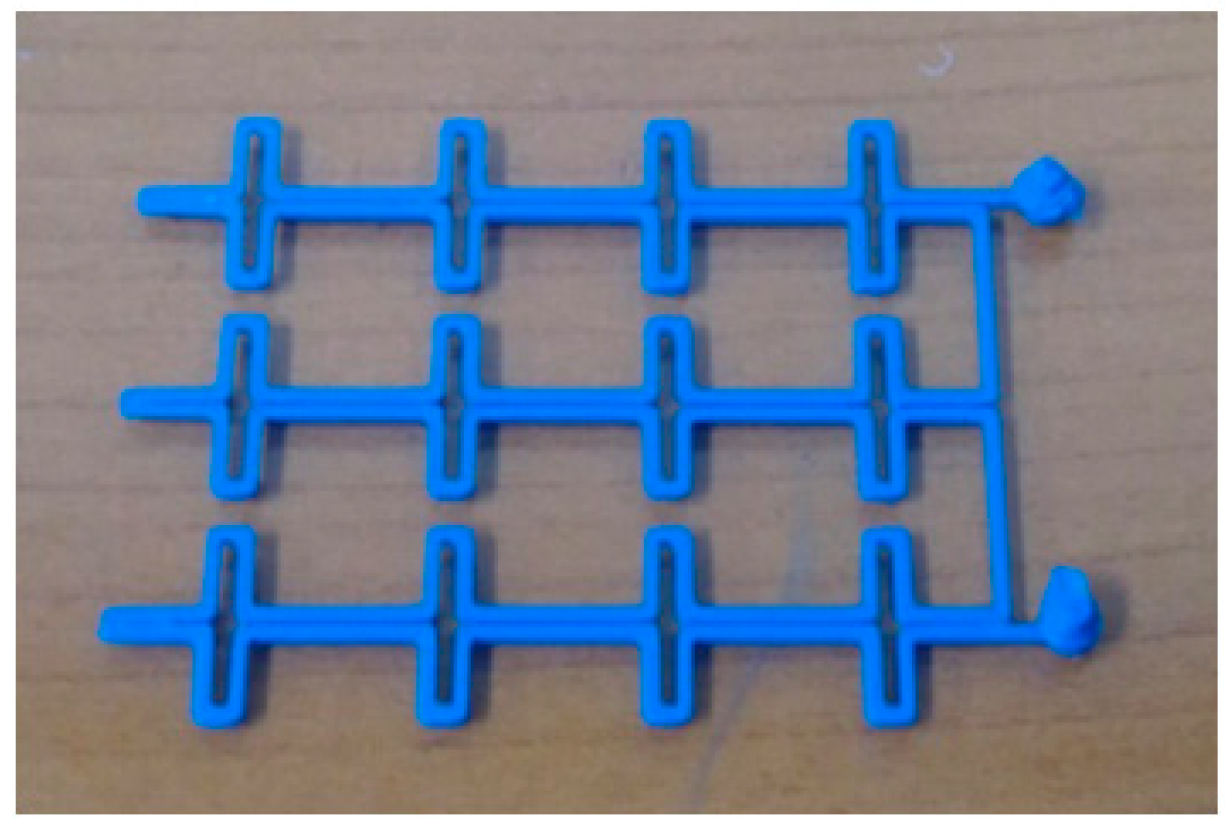
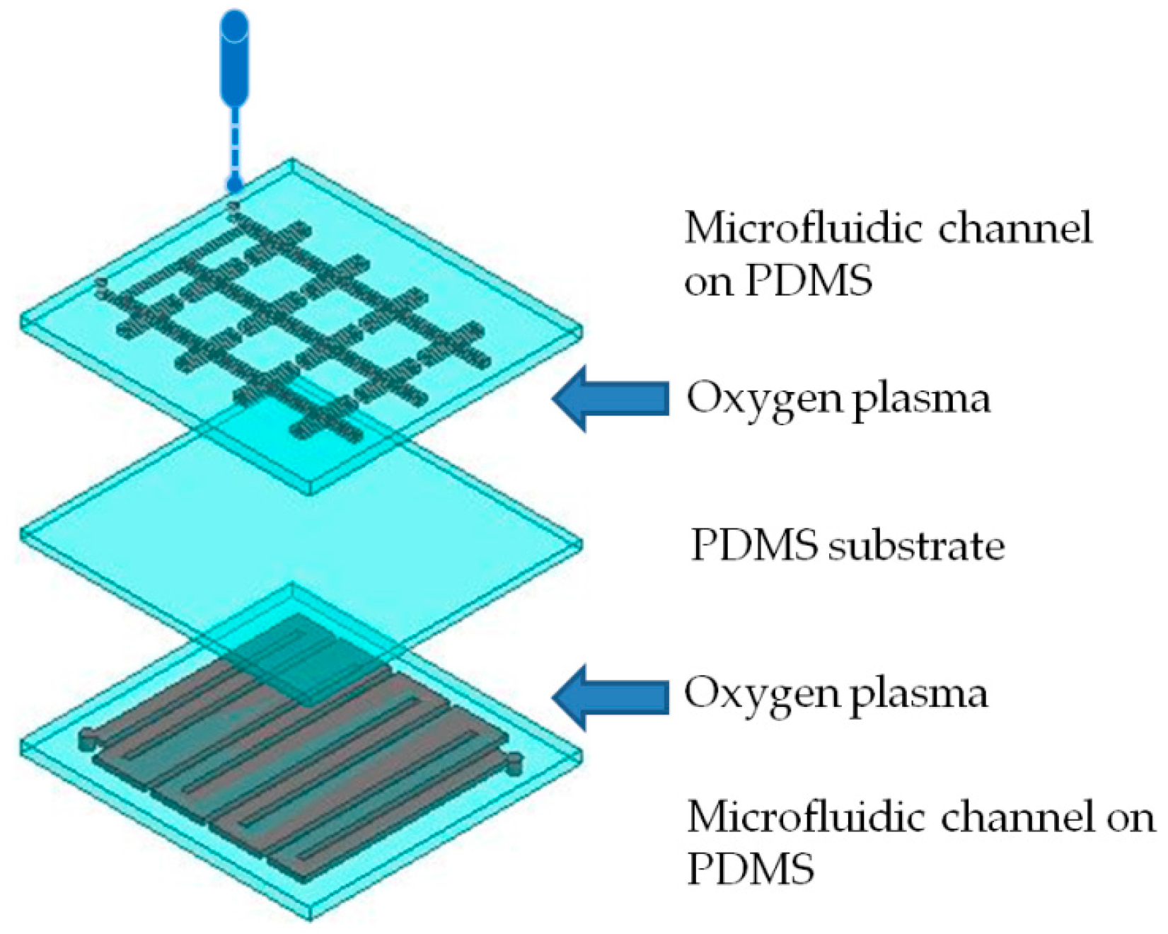
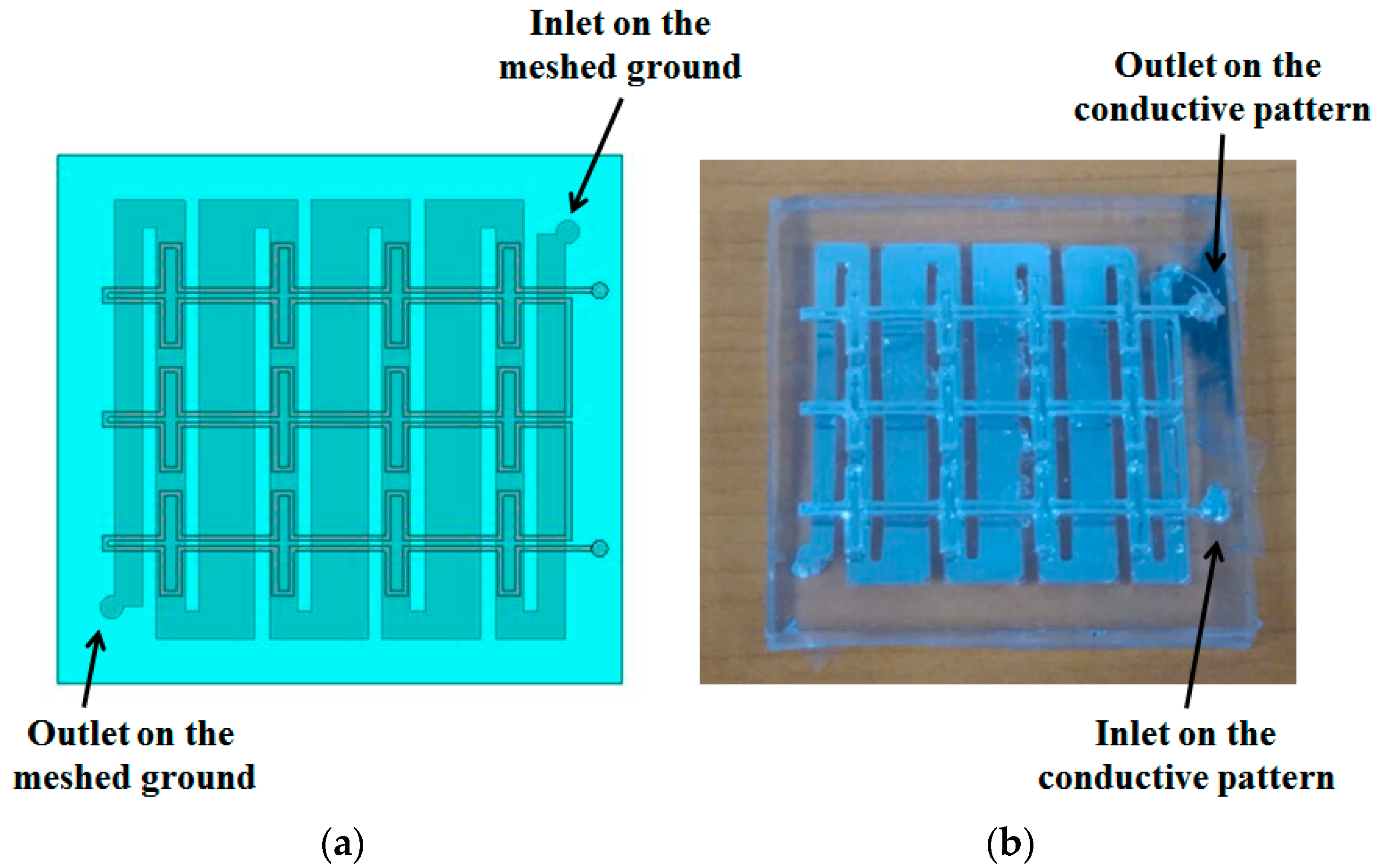
3. Fabrication
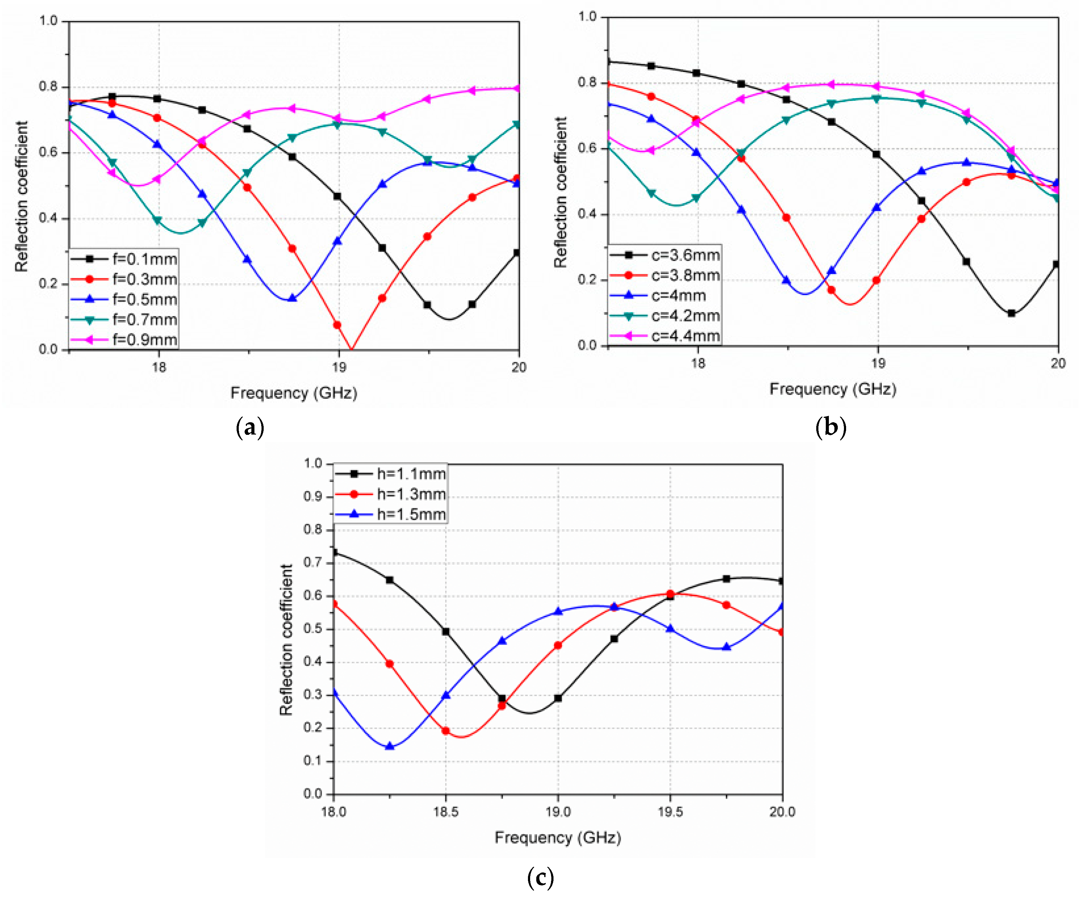
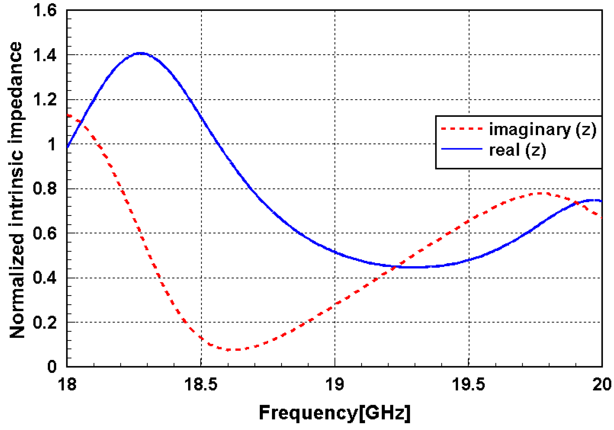
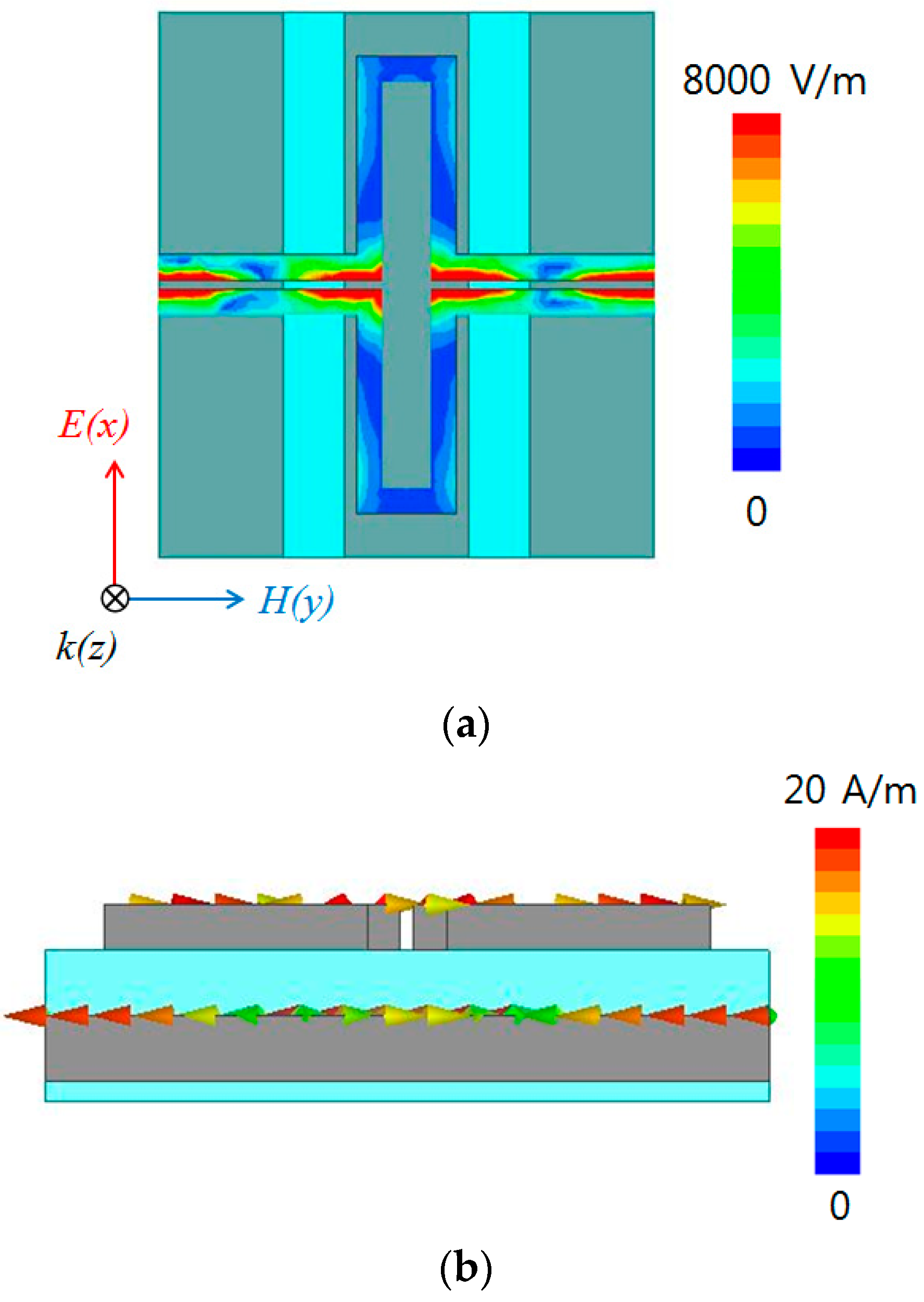
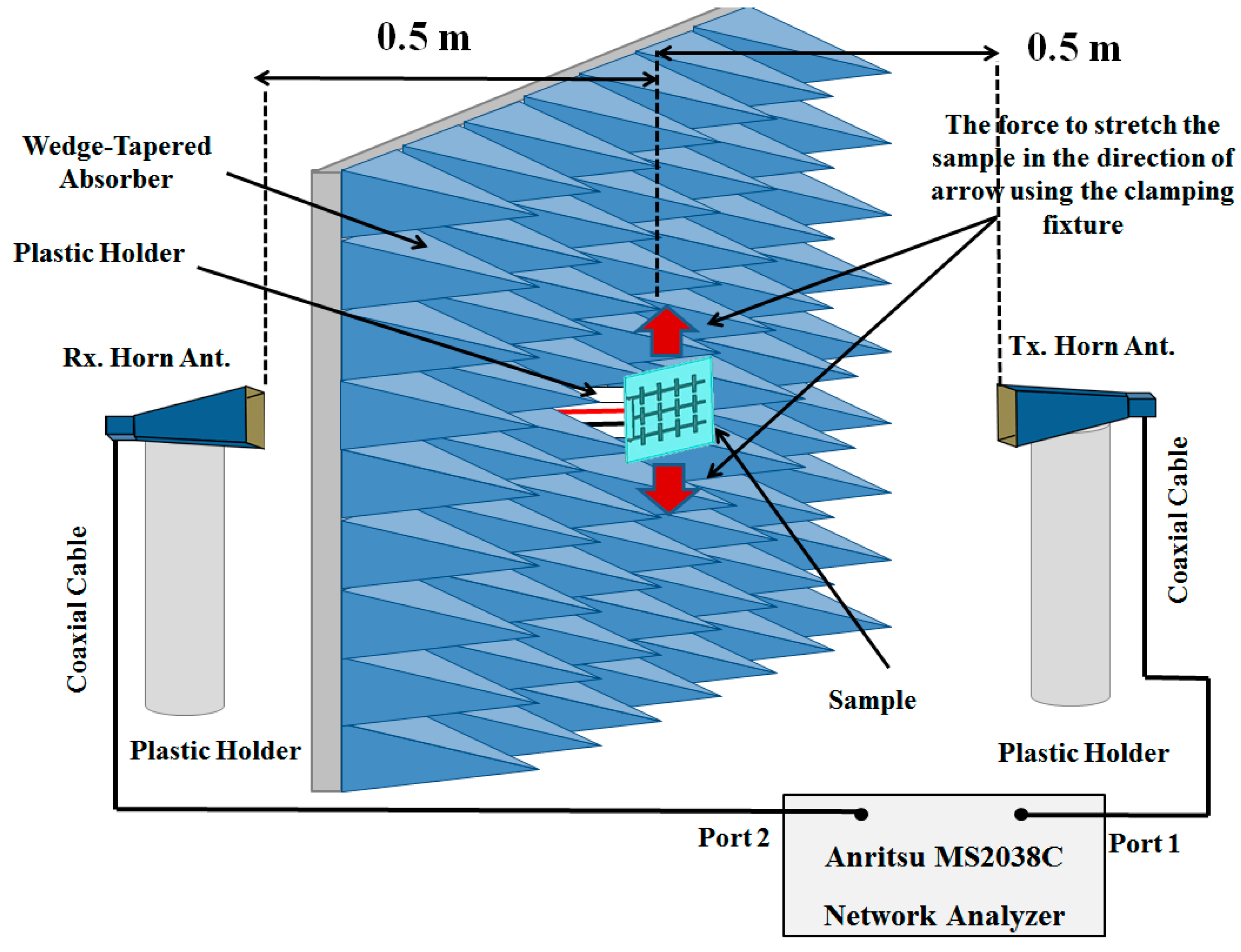
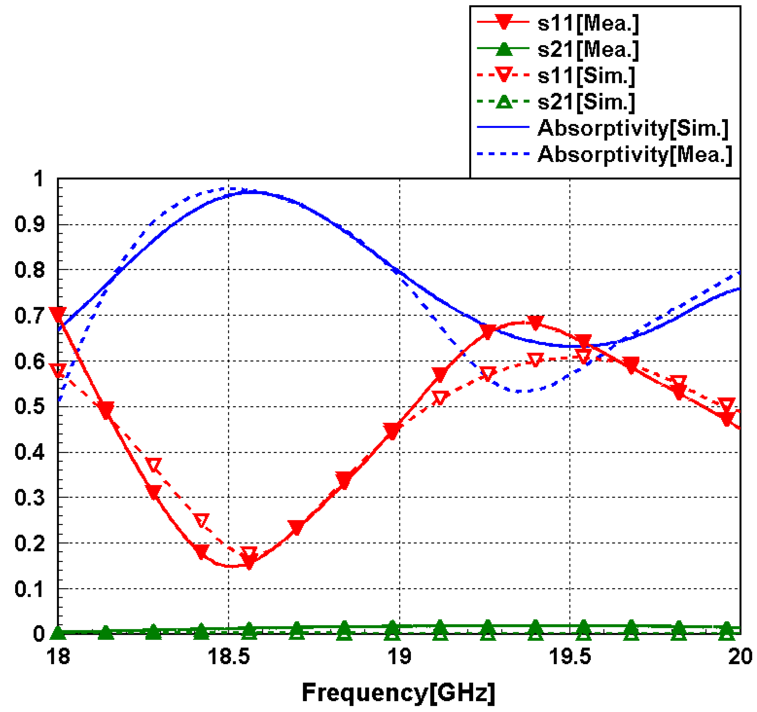
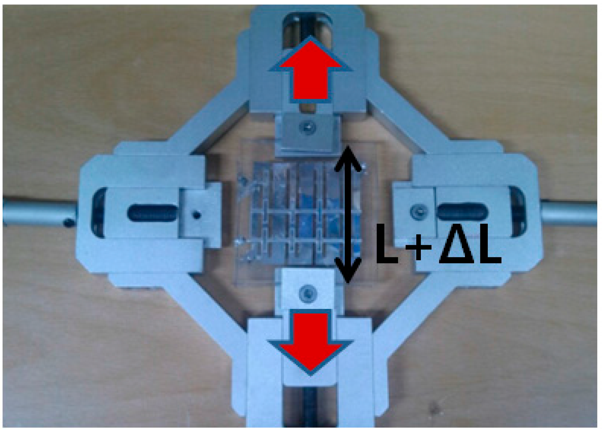
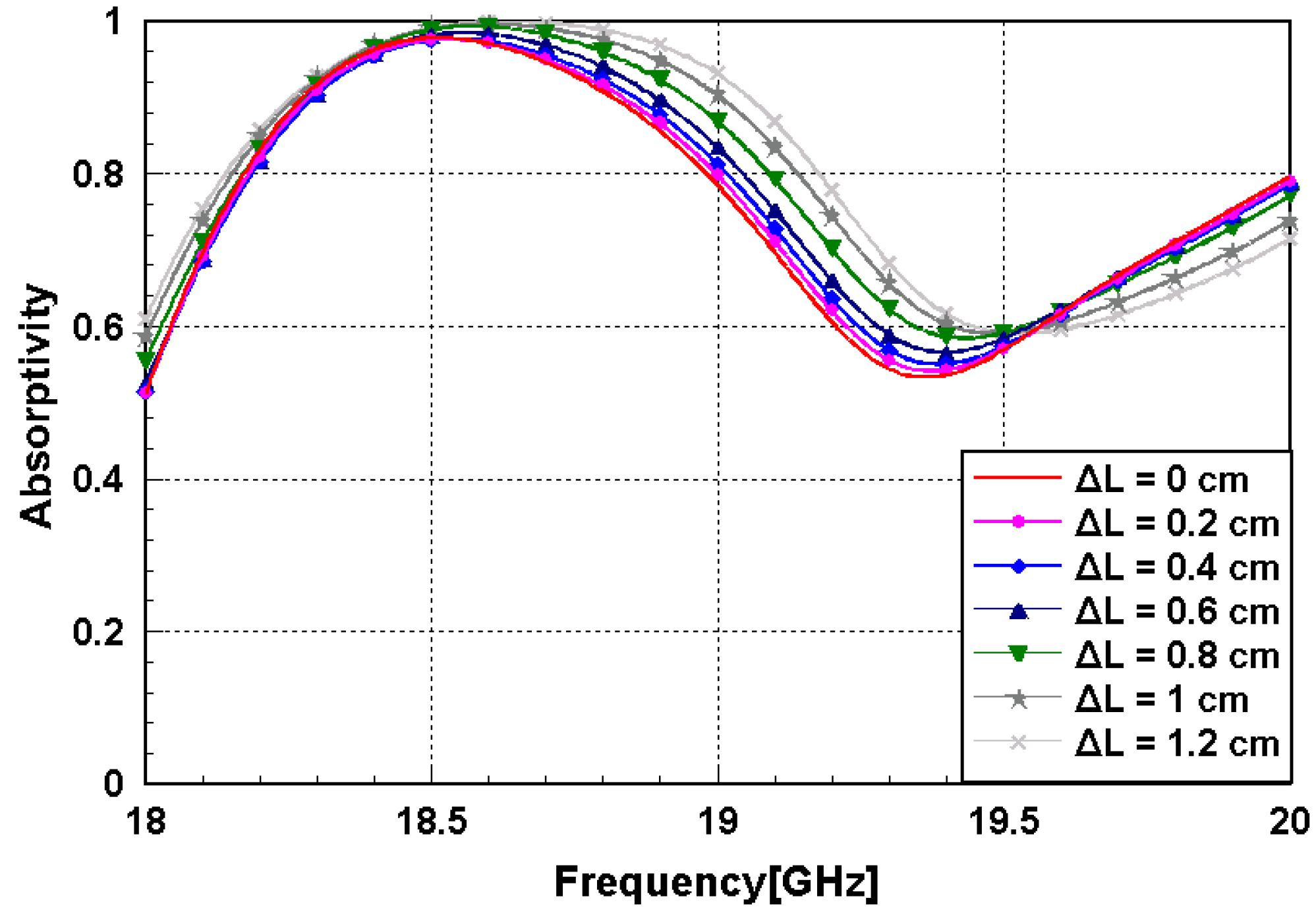
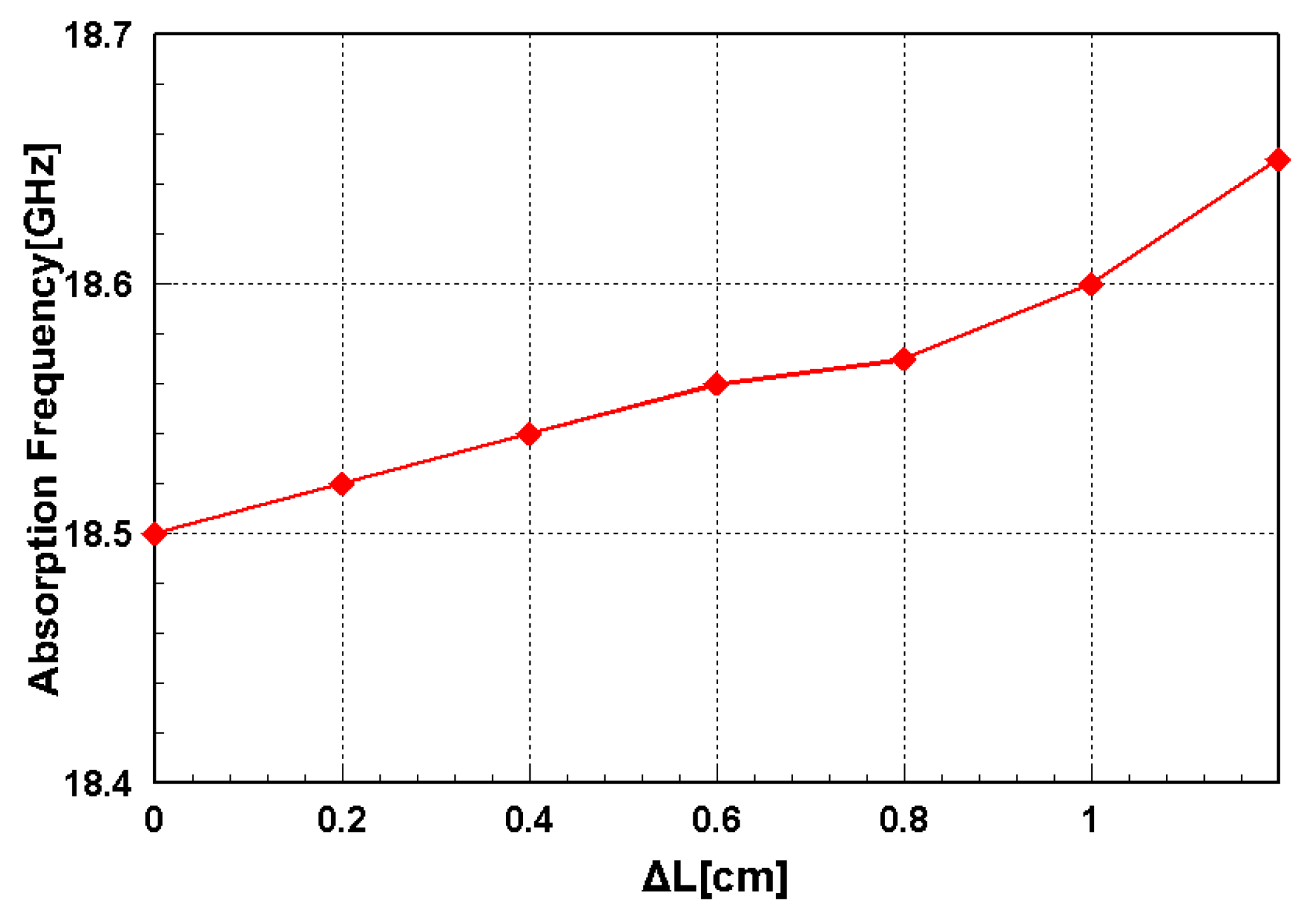
4. Simulation and Measurement Results
5. Conclusions
Acknowledgments
Author Contributions
Conflicts of Interest
References
- Jang, Y.; Yoo, M.; Lim, S. Conformal Metamaterial Absorber for Curved Surface. Opt. Express 2013, 21, 24163–24170. [Google Scholar] [PubMed]
- Yoo, M.; Lim, S. SRR-and CSRR-Loaded Ultra-Wideband (UWB) Antenna with Tri-Band Notch Capability. J. Electromagn. Waves Appl. 2013, 27, 2190–2197. [Google Scholar] [CrossRef]
- Withayachumnankul, W.; Lin, H.; Serita, K.; Shah, C.M.; Sriram, S.; Bhaskaran, M.; Tonouchi, M.; Fumeaux, C.; Abbott, D. Sub-Diffraction Thin-Film Sensing with Planar Terahertz Metamaterials. Opt. Express 2012, 20, 3345–3352. [Google Scholar] [CrossRef] [PubMed]
- Landy, N.; Sajuyigbe, S.; Mock, J.; Smith, D.; Padilla, W. Perfect Metamaterial Absorber. Phys. Rev. Lett. 2008, 100, 207402. [Google Scholar] [CrossRef] [PubMed]
- Noor, A.; Hu, Z. Dual Polarised Wideband Metamaterial Radar Absorbing Screen Based on Resistive Hilbert Curve Array. Electron. Lett. 2009, 45, 130–131. [Google Scholar] [CrossRef]
- Lee, J.; Lim, S. Bandwidth-enhanced and polarisation-insensitive metamaterial absorber using double resonance. Electron. Lett. 2011, 47, 8–9. [Google Scholar] [CrossRef]
- Shen, X.; Cui, T.; Zhao, J.; Ma, H.; Jiang, W.; Li, H. Polarization-independent wide-angle triple-band metamaterial absorber. Opt. Express 2011, 19, 9401–9407. [Google Scholar] [CrossRef] [PubMed]
- Liu, Y.; Gu, S.; Luo, C.; Zhao, X. Ultra-thin broadband metamaterial absorber. Appl. Phys. A 2012, 108, 19–24. [Google Scholar] [CrossRef]
- Li, H.; Yuan, L.; Zhou, B.; Shen, X.; Cheng, Q.; Cui, T. Ultrathin multiband gigahertz metamaterial absorbers. J. Appl. Phys. 2011, 110, 014909. [Google Scholar] [CrossRef]
- Kim, B.K.; Lee, B.S. Design of Metamaterial-Inspired Wideband Absorber at X-Band Adopting Trumpet Structures. J. Elec. Sci. 2014, 14, 314–316. [Google Scholar] [CrossRef]
- Liu, X.; Starr, T.; Starr, A.; Padilla, W. Infrared spatial and frequency selective metamaterial with near-unity absorbance. Phys. Rev. Lett. 2010, 104, 207403. [Google Scholar] [CrossRef] [PubMed]
- Liu, N.; Mesch, M.; Weiss, T.; Hentschel, M.; Giessen, H. Infrared perfect absorber and its application as plasmonic sensor. Nano Lett. 2010, 10, 2342–2348. [Google Scholar] [CrossRef] [PubMed]
- Hao, J.; Wang, J.; Liu, X.; Padilla, W.; Zhou, L.; Qiu, M. High performance optical absorber based on a plasmonic metamaterial. Appl. Phys. Lett. 2010, 96, 251104. [Google Scholar] [CrossRef]
- Kang, H.; Lim, S. High isolation transmitter and receiver antennas using high-impedance surfaces for repeater applications. J. Electromagn. Waves Appl. 2013, 27, 2281–2287. [Google Scholar] [CrossRef]
- Iwaszczuk, K.; Strikwerda, A.; Fan, K.; Zhang, X.; Averitt, R.; Jepsen, P. Flexible metamaterial absorbers for stealth applications at terahertz frequencies. Opt. Express 2012, 20, 635–643. [Google Scholar] [CrossRef] [PubMed]
- Tao, H.; Bingham, C.; Strikwerda, A.; Pilon, D.; Shrekenhamer, D.; Landy, N.; Fan, K.; Zhang, X.; Padilla, W.; Averitt, R. Highly flexible wide angle of incidence terahertz metamaterial absorber: Design, fabrication, and characterization. Phys. Rev. B 2008, 78, 241103. [Google Scholar] [CrossRef]
- Alves, F.; Grbovic, D.; Kearney, B.; Karunasiri, G. Microelectromechanical Systems Bimaterial Terahertz Sensor with Integrated Metamaterial Absorber. Opt. Lett. 2012, 37, 1886–1888. [Google Scholar] [CrossRef] [PubMed]
- Melik, R.; Unal, E.; Perkgoz, N.K.; Puttlitz, C.; Demir, H.V. Metamaterial-Based Wireless Strain Sensors. Appl. Phys. Lett. 2009, 95. [Google Scholar] [CrossRef]
- Zhao, J.; Cheng, Q.; Chen, J.; Qi, M.Q.; Jiang, W.X.; Cui, T.J. A Tunable Metamaterial Absorber using Varactor Diodes. New J. Phys. 2013, 15. [Google Scholar] [CrossRef]
- Zhu, B.; Feng, Y.; Zhao, J.; Huang, C.; Jiang, T. Switchable Metamaterial Reflector/Absorber for Different Polarized Electromagnetic Waves. Appl. Phys. Lett. 2010, 97. [Google Scholar] [CrossRef]
- Yoo, M.; Lim, S. Active Metasurface for Controlling Reflection and Absorption Properties. Appl. Phys. Express 2014, 7. [Google Scholar] [CrossRef]
- Ling, K.; Yoo, M.; Su, W.; Kim, K.; Cook, B.; Tentzeris, M.M.; Lim, S. Microfluidically Tunable Paper-Based Inkjet-Printed Metamaterial Absorber. Opt. Express 2015, 23, 110–120. [Google Scholar] [CrossRef] [PubMed]
- Tiercelin, N.; Coquet, P.; Sauleau, R.; Senez, V.; Fujita, H. Polydimethylsiloxane Membranes for Millimeter-Wave Planar Ultra Flexible Antennas. J Micromech. Microeng. 2006, 16, 2389. [Google Scholar] [CrossRef]
- McDonald, J.C.; Metallo, S.J.; Whitesides, G.M. Fabrication of a Configurable, Single-Use Microfluidic Device. Anal. Chem. 2001, 73, 5645–5650. [Google Scholar] [CrossRef] [PubMed]
- So, J.; Thelen, J.; Qusba, A.; Hayes, G.J.; Lazzi, G.; Dickey, M.D. Reversibly Deformable and Mechanically Tunable Fluidic Antennas. Adv. Funct. Mater. 2009, 19, 3632–3637. [Google Scholar] [CrossRef]
- Whitesides, G.M. The Origins and the Future of Microfluidics. Nature 2006, 442, 368–373. [Google Scholar] [CrossRef] [PubMed]
- Smith, D.; Vier, D.; Koschny, T.; Soukoulis, C. Electromagnetic parameter retrieval from inhomogeneous metamaterials. Phys. Rev. E 2005, 71, 036617. [Google Scholar] [CrossRef] [PubMed]
- Hwang, Y.; Paydar, O.H.; Candler, R.N. 3D printed molds for non-planar PDMS microfluidic channels. Sens. Actuators A Phys. 2015, 226, 137–142. [Google Scholar] [CrossRef]
- Chan, H.N.; Chen, Y.; Shu, Y.; Chen, Y.; Tian, Q.; Wu, H. Direct, one-step molding of 3D-printed structures for convenient fabrication of truly 3D PDMS microfluidic chips. Microfluid. Nanofluid. 2015, 19, 9–18. [Google Scholar] [CrossRef]
- Isiksacan, Z.; Guler, M.T.; Aydogdu, B.; Bilican, I.; Elbuken, C. Rapid fabrication of microfluidic PDMS devices from reusable PDMS molds using laser ablation. J. Micromech. Microeng. 2016, 26, 035008. [Google Scholar] [CrossRef]
- Anderson, J.R.; Chiu, D.T.; Jackman, R.J.; Cherniavskaya, O.; McDonald, J.C.; Wu, H.; Whitesides, S.H.; Whitesides, G.M. Fabrication of topologically complex three-dimensional microfluidic systems in PDMS by rapid prototyping. Anal. Chem. 2000, 72, 3158–3164. [Google Scholar] [CrossRef] [PubMed]
- Govindaraju, A.; Chakraborty, A.; Luo, C. Reinforcement of PDMS masters using SU-8 truss structures. J. Micromech. Microeng. 2005, 15, 1303. [Google Scholar] [CrossRef]
- Bhattacharya, S.; Datta, A.; Berg, J.M.; Gangopadhyay, S. Studies on surface wettability of poly (dimethyl) siloxane (PDMS) and glass under oxygen-plasma treatment and correlation with bond strength. J. Microelectromech. Syst. 2005, 14, 590–597. [Google Scholar] [CrossRef]
- Li, T.Y.; Wang, L.; Wang, J.M.; Li, S.; He, X.J. A Dual band polarization-insensitive tunable absorber based on terahertz MEMS metamaterial. Integr. Ferroelectr. 2014, 151, 157–163. [Google Scholar] [CrossRef]
- Savo, S.; Shrekenhamer, D.; Padilla, W.J. Liquid crystal metamaterial absorber spatial light modulator for THz applications. Adv. Opt. Mater. 2014, 2, 275–279. [Google Scholar] [CrossRef]
- Dincer, F. Electromagnetic energy harvesting application based on tunable perfect metamaterial absorber. J. Electromagn. Waves Appl. 2015, 5071, 1–10. [Google Scholar] [CrossRef]
- Ling, K.; Yoo, M.; Lim, S. Frequency Tunable Metamaterial Absorber using Hygroscopicity of Nature Cork. IEEE Antennas Wirel. Propag. Lett. 2015, 14, 1598–1601. [Google Scholar] [CrossRef]


| Literature | Tuning Technology | Peak Absorptivity | 80% Absorption BW | TR |
|---|---|---|---|---|
| [34] | MEMS switch | 98% | 0.1 THz (2.7%) | 8.1% |
| [35] | Liquid crystal | 93% | 0.26 THz (7%) | 7.4% |
| [36] | Varactor diode | 99% | 0.1 GHz (0.9%) | 2.2% |
| Proposed work | Stretchable | 98% | 0.8 GHz (4.3%) | 0.8% |
© 2016 by the authors; licensee MDPI, Basel, Switzerland. This article is an open access article distributed under the terms and conditions of the Creative Commons by Attribution (CC-BY) license (http://creativecommons.org/licenses/by/4.0/).
Share and Cite
Kim, K.; Lee, D.; Eom, S.; Lim, S. Stretchable Metamaterial Absorber Using Liquid Metal-Filled Polydimethylsiloxane (PDMS). Sensors 2016, 16, 521. https://doi.org/10.3390/s16040521
Kim K, Lee D, Eom S, Lim S. Stretchable Metamaterial Absorber Using Liquid Metal-Filled Polydimethylsiloxane (PDMS). Sensors. 2016; 16(4):521. https://doi.org/10.3390/s16040521
Chicago/Turabian StyleKim, Kyeongseob, Dongju Lee, Seunghyun Eom, and Sungjoon Lim. 2016. "Stretchable Metamaterial Absorber Using Liquid Metal-Filled Polydimethylsiloxane (PDMS)" Sensors 16, no. 4: 521. https://doi.org/10.3390/s16040521