2. Materials and Methods
Wear of micro end mills is mainly confined to the cutting edges. This is the reason why a single cutting edge design is ideal for research on tool wear. Every material removal has to be conducted by this cutting edge and thus, the behavior can be studied in depth. The single edge design chosen for this research was derived from the micro end mill design in
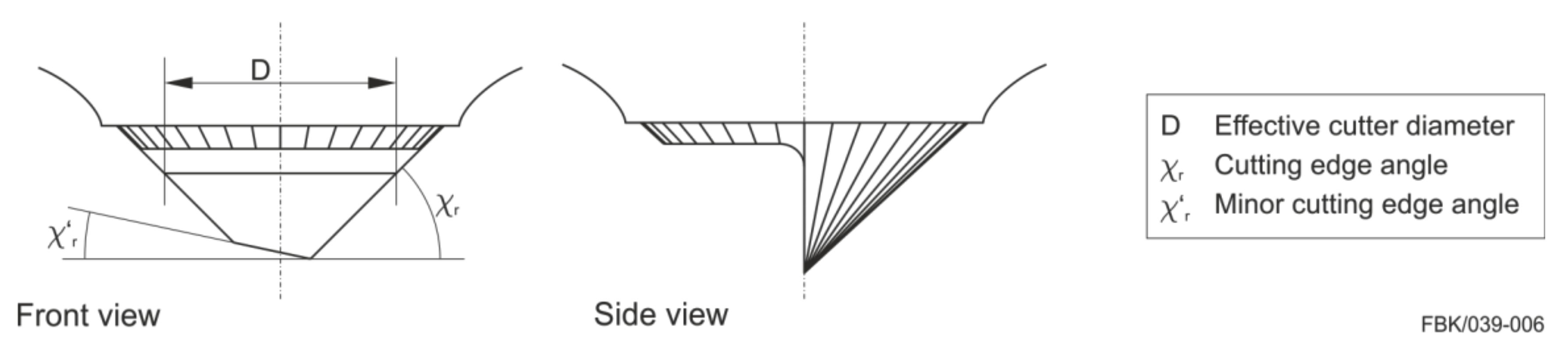
Figure 1.
The micro end mill in this research had a minor cutting edge angle χ’r of 12° and was optimized for a feed per tooth up to 3 µm. The cutting edge angle χr was 45°.
These micro end mills were made of cemented carbide with a grain size of 0.2 µm, 91% wolfram carbide, and 9% cobalt, a hardness of 1950 HV30 and a transverse rupture strength of 4700 N/mm
2. Its manufacture was conducted after [
9] on a LT-Ultra MTC2501 (LT-Ultra Precision Technology GmbH, Aftholderberg, Germany) ultra-precision lathe. The ultra-precision lathe has a massive granite machine bed with hydrostatic axes in
x- and
z-directions. The straightness of the
x-axis is 0.14 µm with a travel of 251 mm and straightness of the
z-axis is 0.1 µm with a travel of 255 mm. The
c-axis is an air bearing rotary axis with a maximum spindle speed of 2500 rpm, an axial spindle error of 0.051 µm and a run-out of 0.053 µm.
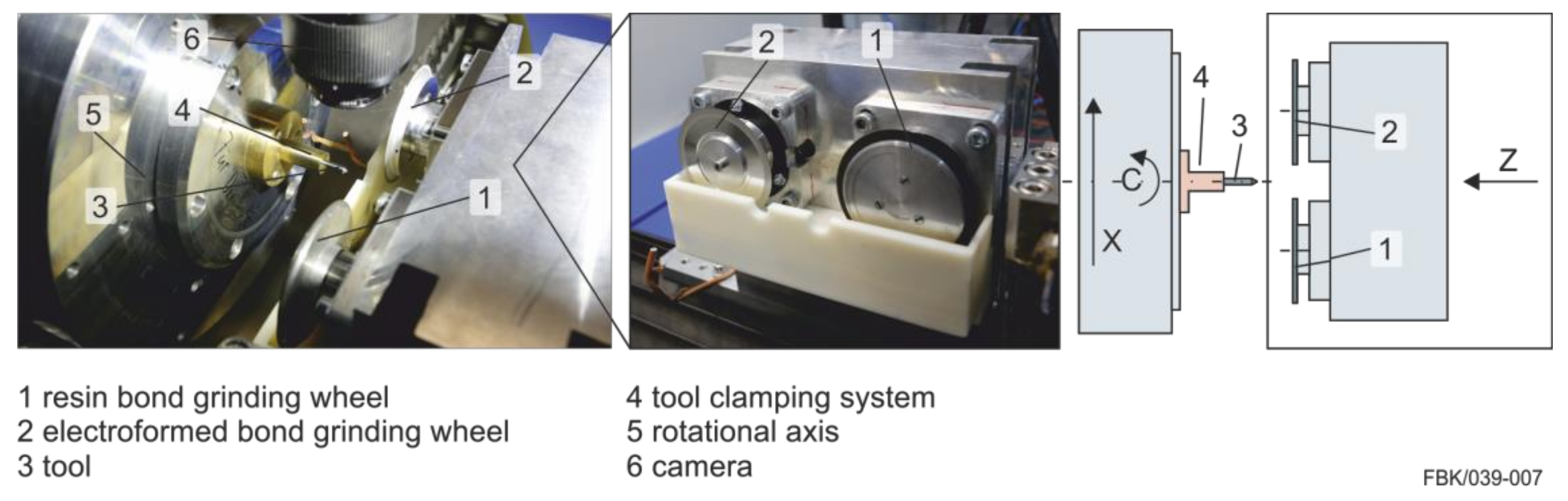
For tool manufacturing, a cemented carbide blank is mounted in the shrink fit chuck that guarantees a low run-out error on the
c-axis of the machine tool (rotary axis). On the
z-axis, two hydrodynamic spindle motors hold the diamond grinding wheels (
Figure 2). These motors have low vibrations and as a result, a low run-out of <0.8 µm at a spindle speed of 12,500 rpm [
10]. For the pre-grinding process, a resin bond grinding wheel with mesh #800 and a thickness of 250 µm was used. The grinding wheel for fine grinding was an electroplated bond with mesh #4800 and a thickness of 50 µm. The process steps of the tool manufacturing are shown in
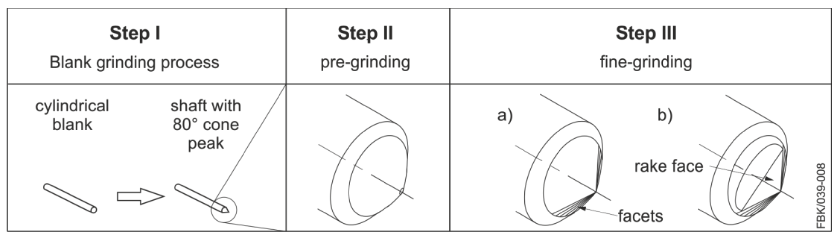
Figure 3.
Step 1 was conducted on a conventional tool grinding machine. The reason for this is the high amount of material to be removed to produce the cone on the tool blank. After this step, the blank with the cone tip was mounted in the shrink fit chuck on the ultra-precision lathe. Step 2 was performed with the resin bond grinding wheel to realize a comparably high material removal whereas Step 3 was performed with the fine grinding wheel to produce the desired geometry as accurately and smooth as possible. The facets shown in Step 3 were necessary because the ultra-precision lathe does not offer any free form generation (three-axis machine tool). Thus, the ideal geometry is approximated by linear movements resulting in these facets.
After grinding, the micro end mills were coated. Eight different coatings were examined: TiN, AlTiN, Al
2O
3, TiB
2, DLC (diamond like carbon), W-C:H, electroless plated diamond, and diamond (via CVD—chemical vapor deposition). The DLC coating as well as the diamond (CVD) were provided by an external supplier, all other were made in-house: TiN, AlTiN, W-C:H, and TiB2 were produced in a physical vapor deposition (PVD) process with an Oerlikon Metco Domino Mini
1 system. Al
2O
3 was produced by a Picosun R-series atomic layer deposition reactor
1. The electroless plated diamond tools were produced with a system derived from [
11].
TiN has a hardness of 2100 HV [
12]. It is applied on the cemented carbide by means of a titanium interface layer. The interface layer increases adhesion. During the titanium coating, the addition of nitrogen is slowly increased, which results in a graded layer with its highest hardness on the surface. The coating thickness was 2.5 µm.
The addition of aluminum to TiN results in an increased heat insulation of the tool; this protects the tool from damaging heat input which evolves in the contact zone due to friction and cutting [
13]. This AlTiN coating is also harder than TiN with 3300 HV [
14] and has already been successfully applied in previous works for micro milling applications [
5]. The applied AlTiN had a thickness of 2.5 µm
Titanium based coatings form compounds with the oxygen in the environment on the surface and thus lead to the formation of titanium oxide (TiO
2) and, in the case of AlTiN, also to Al
2O
3. Both TiO
2 and Al
2O
3 layers are softer than the Ti-based coating itself. This decomposition is a downside of Ti-coatings and leads to increased wear of the coating [
15].
Al
2O
3 as a coating has a high resistance to oxidative wear due to the oxygen bound in the coating forming a stable composition [
16]. Al
2O
3 is chemically inert and has a low thermal conductivity. The thermal conductivity property predestines Al
2O
3 as a coating for the thermal insulation of the tool [
17]. With its hardness of 2300 HV [
12], Al
2O
3 can additionally protect against abrasive wear. The Al
2O
3 coating thickness was 1 µm.
TiB
2 (titanium diboride) is a ceramic coating characterized by a high hardness of 4000 HV and chemical inertness [
18]. The high hardness combined with a lower coefficient of friction (compared to TiN [
18]) leads to the fact that this layer is highly wear-reducing. A challenge is the low adhesion to the substrate due to high residual compressive stresses in the coating [
18]. However, as it is a titanium based coating, no additional adhesion layer has to be used, which makes it possible to produce hard and thin single layer coatings. The TiB2 coating thickness was 0.2 µm, as determined as optimal thickness in [
19].
Carbon-based coatings were also examined in this research, the so called diamond like carbon coatings (DLC), which W-C:H also belongs to. These layers are amorphous coatings with a predominant component of carbon and low hydrogen content. The amount of sp
2-hybridized carbon leads to a low coefficient of sliding friction and at the same time a low hardness of the coating (1500 HV softer than the carbide substrate). This coating can act as a solid lubricant component. The reduction of friction in the contact zone can thus contribute to reducing abrasive wear [
20]. DLC had a coating thickness of 3 µm and W-C:H had a thickness of 1.3 µm.
When it comes to diamond as a coating layer, diamond is a standard abrasive layer for grinding applications. This diamond is available in different sizes, which makes it also possible to be used in micro grinding applications. Here, the diameter of the diamond particles is much lower than 10 µm, down to the nanometer range, and the diamond is bonded to the cemented carbide by nickel with an electroless plating process [
11]. This process can also be used to coat micro end mills. Due to the small particles, the cutting edge radius stays sharp and is protected against abrasive wear by the inert hardness of diamond. As it is the hardest material available, abrasive wear is low when machining non-iron materials. A downside of this electroless diamond coating is the nickel bond, which makes the layer softer. The electroless plated diamond thickness was 1.9 µm.
To increase the hardness, the cemented carbide was coated with diamond directly. This coating, applied via CVD (hereafter called Diamond CVD), has by far the highest hardness. At only slightly below 10,000 HV, it is almost as hard as natural diamond [
21]. The nanocrystalline structure of the coating results in a low surface roughness, which means that less material adhesion is to be expected compared to uncoated tools [
22]. The low surface roughness also ensures good chip flow and quickly dissipates the heat generated in the contact zone during machining [
23]. Additionally, the coating is very resistant to abrasion. The diamaond CVD-coating had a thickness of 2.4 µm.
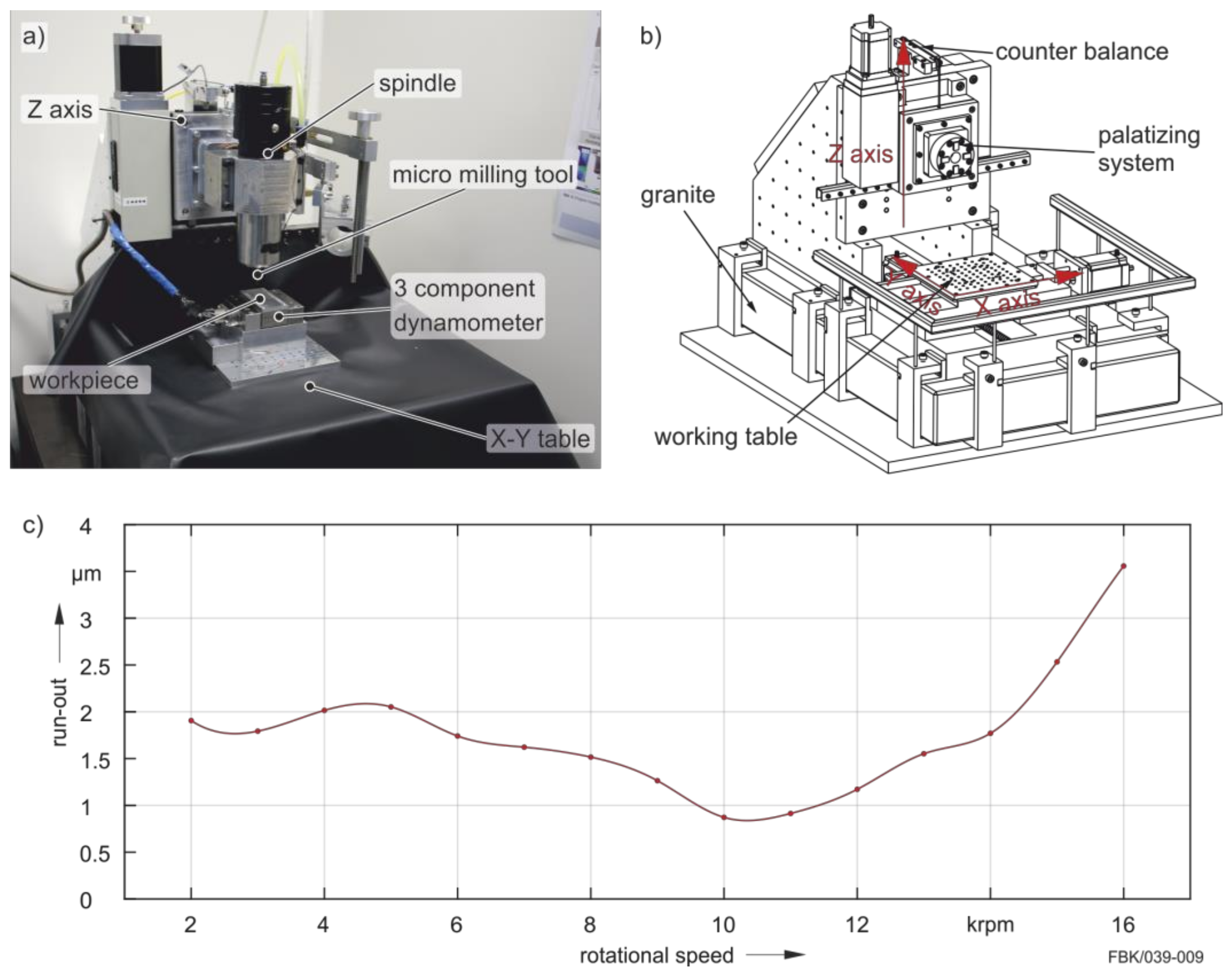
After coating, test cuts were performed on an in-house developed three axes universal precision milling machine (UPMM). This machine tool is built up on a granite machine bed (
Figure 4a,b). Air bearing linear axes are used in
x- and
y-direction with a travel of 140 mm. The
z-direction is realized by a cross roller bearing axis with a travel of 60 mm. All axes are driven by stepper motors realizing an accuracy of <1 µm. On the
z-axis, a palletizing system with a repeatability of about 2 µm is installed. With this system, it is possible to use this machine tool for machining when installing an air bearing spindle or as a measuring machine when installing a confocal microscope. This property makes this machine tool universal for micro machining applications as the process result can be directly measured after machining.
For the test cuts, an ABL MM160
1 (Air Bearings Ltd, Ferndown, United Kingdom) air bearing spindle was used. This spindle can reach a spindle speed between 20,000 and 160,000 rpm with the characteristic shown in
Figure 4c. The test cuts were performed at 90,000 rpm, thus the run-out at the tool tip was about 1.5 µm (peak-to-peak). The spindle speed was chosen, as it is an area with an average run-out error. This means that there is impact load on the micro end mill as well as the coating. When the micro end mill as well as the coating are able to withstand this, they are also capable of machining with a lower run-out error. On the other hand, if the run-out error is too high, tool breakage is very likely, thus preventing the evaluation of the coating’s performance. All micro end mills were designed for a run-out of 3 µm which means there should be no unwanted contact between micro end mill and material to be cut (only the cutting edge penetrates the workpiece material). The feed per tooth was f
z = 2 µm and the depth of cut a
p = 25 µm. This chip load in combination with the depth of cut is a proven parameter at our lab. It is a good compromise between surface quality, process stability, and tool wear. Lower feed rates result in higher ploughing and thus the tool wear increases. Higher feed rates result in higher stress levels of the tools which may result in tool breakage.
Each tool was tested in brass (CuZn40Pb2) with a travel path of only 200 mm to examine the initial wear. Brass was chosen as it is a common material in micro machining and often large areas need to be machined without tool change to keep the precision of the structure. Hence, tool wear is very crucial for machining these structures.
To reach the travel path of 200 mm, slots with a length of 25 mm were machined in brass with alternating feed direction. All machining tests were conducted without metal working fluids in a clean room environment with a temperature stability of ±0.5 K.
3. Results
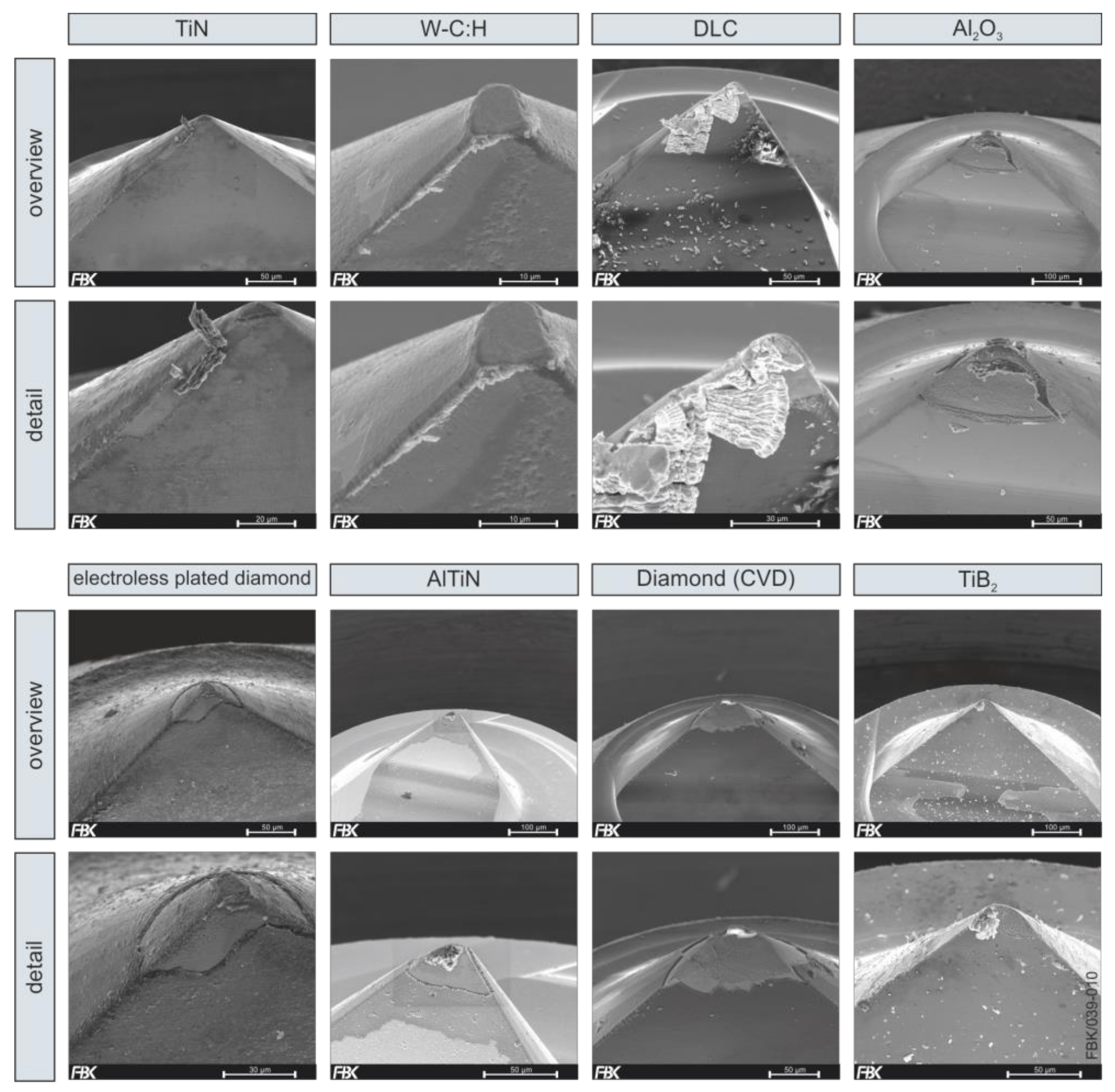
The test cuts showed three different types of wear of the coatings (
Figure 5). The TiN and the W-C:H coatings provided adequate adhesion on the cemented carbide of the micro end mill. However, they were not hard enough to withstand the machining conditions, thus they showed abrasive wear at the cutting edge and on the rake face. This can be seen in FIB (focused ion beam) cuts for W-C:H in
Figure 6. There, the thickness of the coating varies between 0.52 and 0.16 µm. The initial layer thickness was about 1.3 µm, thus there is not much coating left and the micro end mill wears out relatively fast. The DLC, Al
2O
3, electroless plated diamond and the AlTiN coatings showed an almost immediate flake off. This means the adhesion on the micro end mill was not good enough although the layer itself should be sufficiently hard. In addition, when the Al
2O
3 ripped off, the geometry of the micro end mill was changed. The diamond (CVD) coating showed the same behavior. When the tool started to cut, the tip of the micro end mill broke off. This could be because the coating ripped off or because of the high coating temperatures of this process (>900 °C) which may lead to a change in the material properties of the cemented carbide, causing premature failure.
The TiB
2 coating shows almost no wear after the test cut and no flake off. This means the coating is hard enough to withstand the machining conditions for a longer period of time. In another study, the most suitable layer thickness for this coating was determined [
19]. The layer thickness exhibits two contradicting properties: the thicker the layer, the higher the residual stresses inside the layer (resulting in breakage of the coating); the thinner the layer, the lower the wear resistance. The ideal coating layer thickness for micro milling was determined to be 200 nm.
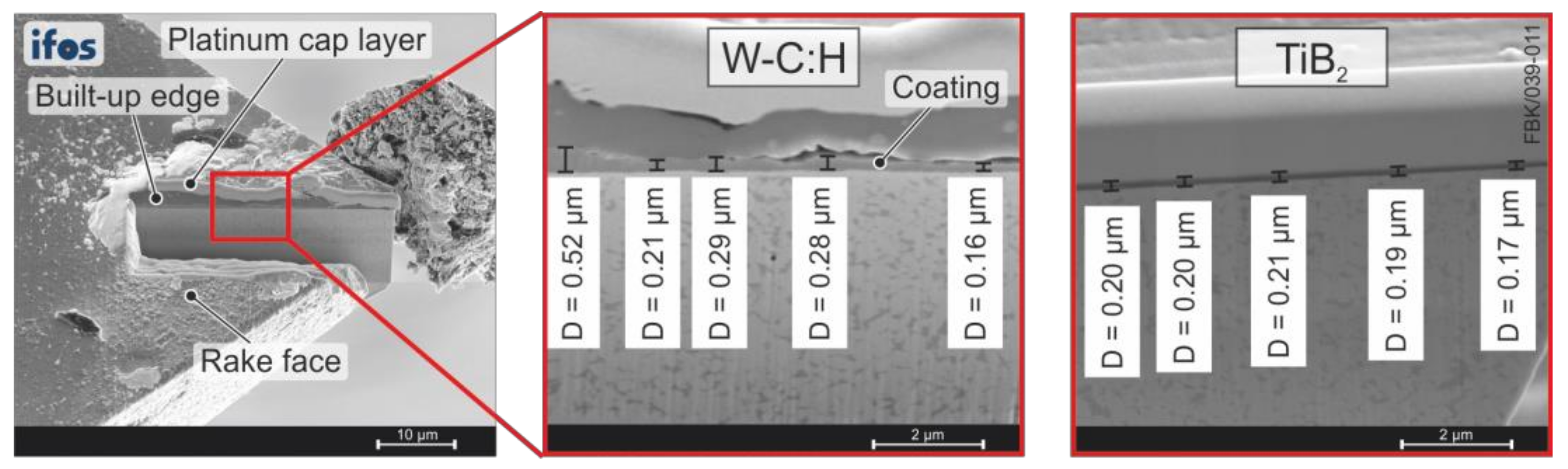
To examine the properties of the best performing layer (TiB
2) on the micro end mill, a FIB cut was done.
Figure 6 shows the wear of a non-functioning W-C:H layer and the TiB
2 coating as a comparison.
Therefore, a cross section cut through the tip of the micro end mill was done by an ALTURA 875 (FEI)
1 DualBeam focused ion beam (FIB). After deposition of a platinum cap layer on the surface to protect the original samples’ topography and to avoid edge rounding, the cross section was cut by a 30 keV gallium ion beam. The cap layer can be seen in the SEM picture of
Figure 6 as white layer, respectively as white bar in the detailed side view SEM picture.
For the W-C:H layer, below the cap layer in the side view of the cross section, an approximately 1 µm thick layer of brass (built-up edge) can be seen. Beneath, the W-C:H layer follows. It still forms a closed layer, but with an inhomogeneous layer thickness. The layer thickness was measured at five different positions of the cross section and varies over this distance from 0.16 μm up to 0.52 μm (unworn layer thickness ~1.3 µm). The existing cavities between the W-C:H layer and the adhered brass layer indicate local detachments of the brass layer. Beneath the W-C:H layer, the cemented carbide structure can be seen.
For the TiB2, a homogeneous layer thickness can be seen. It varied only between 0.17 and 0.21 µm (unworn layer thickness ~0.2 µm). No built-up edge or defects are visible.
For further analysis of the best performing TiB
2 layer, instrumented indentation technique, also called depth sensing indentation, as introduced and described in detail by Oliver and Pharr [
24,
25] was performed. This technique has become widely used for the characterization of mechanical properties on the microscale. Hardness and other material parameters are derived from load and indentation depth data recorded continuously during the indentation procedure. The difficulty in characterizing coatings is associated with identifying the correct indentation load. On the one hand, it is recommended (in this case DIN EN ISO 14577-4 [
26]) to use an indentation load that is small enough to avoid measurements being influenced by the substrate which would reduce the maximum hardness values. On the other hand, the roughness of the TiB
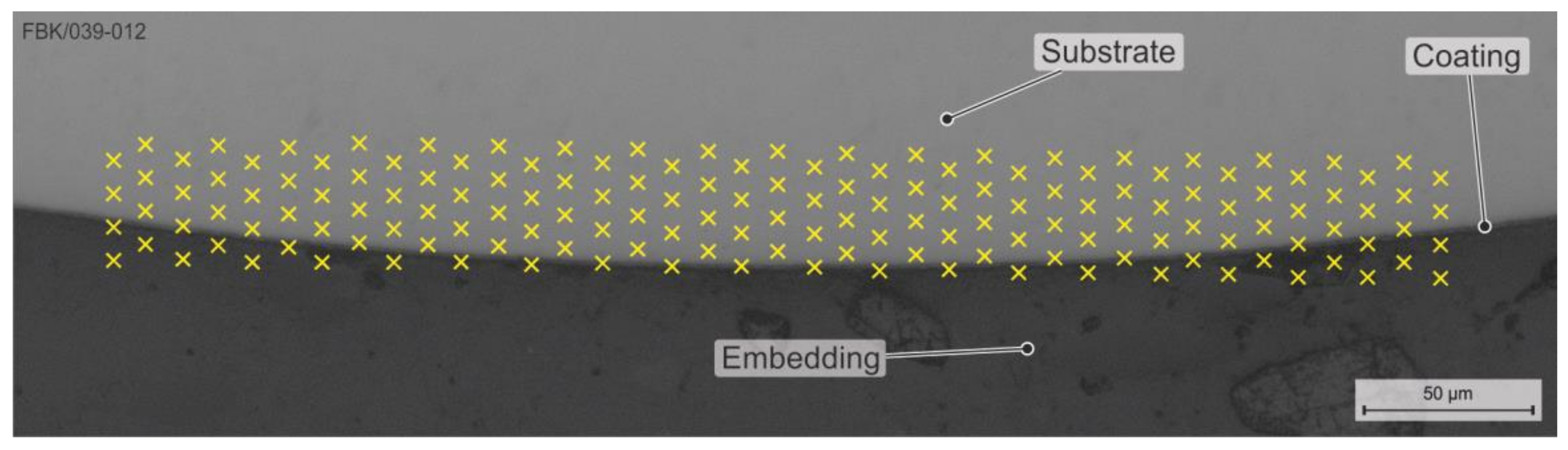
2 coating leads to a deviation of calculated and real contact area and will cause large scatter, especially when the indentation load is small. For these reasons, a polished cross section of the coated micro end mill cemented carbide tool shank was examined. The section was cut out, embedded, and polished with a diamond suspension (particle size down to 0.3 µm). The tests were then performed using the ASMEC Universal Nanomechanical Tester UNAT
1, equipped with a Synton
1 MDP diamond modified Berkovich indenter. In a first step, 156 positions for the indentation tests were set within a rectangular 380 × 35 µm measurement area including embedding, TiB
2 layer and substrate. The positions of the indentations were arranged in 20 rows, each with four indents with a distance of 10 µm to each other. The distance between adjacent columns is 10 µm and an additional 5 µm vertical offset was used to achieve a high resolution perpendicular to the surface of the milling tool as illustrated in
Figure 7.
The testing procedure was as follows: In the loading segment, a linearly increasing loading rate was used to target a maximum value of 50 mN. After a 5 s dwell time, where load was kept constant, the indenter was unloaded again with a constant unloading rate. Then, the so called indentation hardness, which is the quotient of the maximum indentation load and the calculated value of the projected contact area [
27], was derived from the resulting load-indentation depth curve as described in detail in [
28].
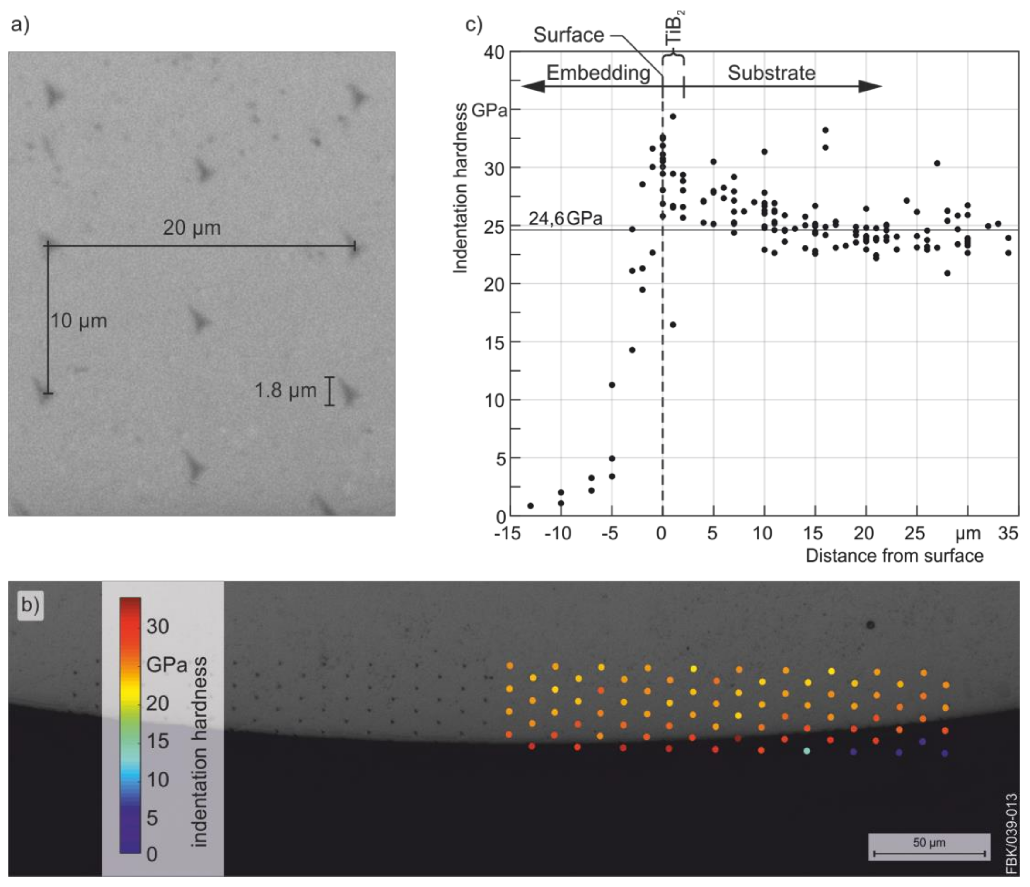
Figure 8a illustrates the dimensions of an indent in the substrate and its distance to neighboring indents. As can be taken from the figure, an indent has a diameter of about 1.8 µm and exhibits a minimum distance of 10 µm to its closest neighbors, as intended.
Figure 8b shows a light microscopy image of the cross section after indentation testing with the indents on the left, as well as superimposed colored dots on the right, with a color scale that indicates the indentation hardness obtained from experimental testing. As can be taken from the figure, hardness values scatter slightly in the substrate and considerably higher values were obtained in close proximity to the surface of the milling tool (i.e., in the TiB
2 layer), whereas the lowest values were obtained in the embedding.
In
Figure 8c, the indentation hardness from all 156 measurements was plotted against the distance from the surface of the milling tool. The data points scatter around a course, which can be divided into three characteristic parts (embedding, TiB
2 layer, substrate). In the first part (embedding), the data points show a steep increase as getting closer to the surface of the milling tool. In the second part (TiB
2 layer), the hardness values reach a global maximum of about 34.4 GPa. Finally, in part three (substrate), the hardness values decrease and data points asymptotically approximate a mean value of about 24.6 GPa.
The indentation tests indicate that the hardness of the TiB
2 coating is in a range of 33 to 35 GPa, which is about 40% larger than the mean value of the substrate. Nevertheless, this value has to be looked at critically. Due to the small thickness of the coating, it is possible that measurements were influenced by the softer substrate or embedding and the exact value of the indentation hardness could be even higher. According to DIN EN ISO 14577-1 [
28], the use of a modified Berkovich indenter allows for an approximation of the Vickers hardness (HV) by multiplying the calculated indentation hardness with a factor of 92.62. Thus, a value of about 3185 HV can be calculated from the maximum indentation hardness measured on the coating and a value of about 2278 HV can be calculated from the mean indentation hardness of the substrate. This means, the TiB
2 coating has a hardness of at least 3185 HV.

 ,
, 


