Wide-Angle Beam-Steering Using an Optical Phased Array with Non-Uniform-Width Waveguide Radiators

1
Department of Electrical Engineering, Korea Advanced Institute of Science and Technology, 291 Daehak-ro, Yuseong-gu 34141, Daejeon, Korea
2
Department of Nanodevice Technology, National NanoFab Center, Korea Advanced Institute of Science and Technology, 291 Daehak-ro, Yuseong-gu 34141, Daejeon, Korea
*
Author to whom correspondence should be addressed.
Photonics 2020, 7(3), 56; https://doi.org/10.3390/photonics7030056
Submission received: 6 July 2020
/
Revised: 27 July 2020
/
Accepted: 30 July 2020
/
Published: 3 August 2020
(This article belongs to the Section Lasers, Light Sources and Sensors)
Abstract
:We demonstrate wide-angle beam-steering using an optical phased array (OPA) with waveguide radiators designed with non-uniform widths to reduce the crosstalk between waveguides. The OPA consists of a silicon based 1 × 16 array of electro-optic phase shifters and end-fire radiators. The 16 radiators were configured with four different widths and a half-wavelength spacing, which can remove the higher-order diffraction patterns in free space. The waveguides showed a low crosstalk of −10.2 dB at a wavelength of 1540 nm. With phase control, the OPA achieved wide beam-steering of over ±80° with a side-lobe suppression of 7.4 dB.
1. Introduction
Optical phased arrays (OPAs) based on silicon photonics are promising for three-dimensional imaging applications because of their compactness, fast scanning speed and low power consumption [1,2]. One of the important requirements for this application is an assured wide beam-steering of a zeroth-order beam, while avoiding an appearance of higher-order diffraction beams. To satisfy this requirement, various methods which can suppress the higher-order grating lobes and side-lobes have been proposed [3,4,5,6,7,8]. Unequally spaced radiator arrays have been employed as the structures which suppress the high-order grating lobes [3,4,5]. These structures, however, disperse the radiation power to the side-lobes, resulting in a reduction in the side-lobe suppression ratio. Another route to forming a single beam is to narrow the pitch of the radiators to within a half-wavelength space, at which the higher-order diffraction peaks disappear in the free space [9]. However, serious crosstalk can occur in such a narrow space between the radiator waveguides. To solve the crosstalk problem, end-fire OPAs have been proposed which use a radiator region with a short-propagation length [6], a bent waveguide array [7] or a non-uniform-width waveguide array [8]. In the later structure [8], wide beam-steering near 180° was demonstrated in a half-wavelength spaced array with non-uniform waveguide widths. For phase control, they used thermo-optic (TO) phase shifters heated by metal lines.
In this paper, we demonstrate a silicon-based 1 × 16 OPA using end-fire radiators with a non-uniform-width waveguide array and p-i-n electro-optic (EO) phase shifter. The beam-steering range of the OPA is over ±80° and the non-uniform waveguide array suppresses the crosstalk between the waveguides below −10.2 dB. This letter also presents a detailed design process based on a numerical investigation of the crosstalk between the nearest neighbouring waveguides.
2. Design and Simulation
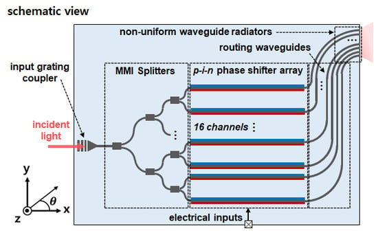
Figure 1a shows a schematic view of the designed OPA. The 1 × 16 OPA consists of an input grating coupler, power splitters, EO phase shifters and non-uniform waveguide radiators. The grating coupler is designed to couple an external light source of 1550 nm wavelength into the OPA chip. The coupled light is distributed into 16 channels through cascading 1 × 2 power splitters based on a multi-mode interferometer (MMI). A 1 mm long p-i-n phase shifter is employed for efficient phase control with high speed and low power consumption at the cost of the current dependent loss [10,11].
Figure 1b shows a cross-sectional view of the non-uniform waveguide radiators we designed. For a given radiator pitch d, the maximum beam-steering angle Δθ of the zeroth-order beam can be determined as [2,9],
where λ0 is the wavelength in the free space. In order to avoid the appearance of higher-order diffraction beams while steering the zeroth-order diffraction beam in whole free space (Δθ = ±90°), the pitch d between the waveguide radiators are designed as 775 nm, based on Equation (1), which corresponds to a half-wavelength (λ0/2) in the free space.
In such densely spaced waveguides, crosstalk occurs not only between the nearest neighbouring waveguides but also between the waveguides having a distance, when the waveguides have uniform widths. To effectively reduce the crosstalk, we determined the number of waveguide widths as four. This allowed simple array construction, which is generally a multiple of four. In addition, assuming that the non-uniform waveguide array already had sufficient width difference, the crosstalk between the nearest neighbouring waveguides should have little effect on the other waveguides [12]. This made it possible to select the widths of the non-uniform waveguides by considering only the interference with the nearest neighbouring waveguides.
To determine the waveguide widths, w1, w2, w3 and w4, we analysed the crosstalk between two parallel waveguides with different widths. These two waveguides consist of a main and a side waveguide. When the light is incident to the main waveguide, the ratio of transferred power from the main to side waveguide, ΔP/Pin, can be expressed as [12,13]:
where Pin is the incident power to the main waveguide, ΔP is the transferred power to the side waveguide, Δβ is the propagation constant difference, C is the coupling coefficient and L is the propagation length. The maximum crosstalk to the side waveguide is defined as 1/[1 + (Δβ/2C)2] which occurs at the cross-over length, L = Lc. From Equation (1), the crosstalk can be reduced by increasing Δβ or decreasing C, which are a function of the waveguide width and pitch. At a fixed pitch, Δβ can increase when the difference in waveguide widths increases, and thus the crosstalk can be reduced. However, if the width of the main waveguide is too narrow, the crosstalk increases, due to the increase in C produced by the spread of the transversal field. This makes it necessary to find an optimal range of width difference Δw.
To determine the appropriate value of Δw, we simulated the crosstalk between the two parallel waveguides. Figure 2 shows the simulation results for the maximum crosstalk, 1/[1 + (Δβ/2C)2], plotted in contour along the varying widths of the two waveguides, at a wavelength of 1550 nm. Lumerical MODE Solutions was used for the simulation. The spacing between the waveguides was fixed at 775 nm, and the height of the waveguide was set at 220 nm. Since the cross-over length, Lc, changes depending on the waveguide width, to calculate the maximum transferred power the length of the waveguide was set to be 2Lc. The light is incident to the main waveguide with a power of Pin, and the coupling of power to the side waveguide ΔP was observed.
Based on a fully vectorial approach using an eigenmode expansion method, the power coupling ratio ΔP/Pin along the propagation length L was calculated [13]. Then, the maximum transferred power ratio, 1/[1 + (Δβ/2C)2], was extracted from ΔP/Pin and plotted in a contour. In Figure 2, the largest crosstalk appears when the widths of the main and the side waveguide are similar, as seen in the yellow zone along the diagonal line.
In a more detailed variation, the contours in Figure 2 show that relatively larger crosstalk occurs when the main waveguide becomes narrower than the side waveguide, rather than the reverse case. This trend can be attributed to the expansion of the evanescent mode of the main waveguide where the light is incident. When the width of the main waveguide is narrower than that of the side waveguide, the wide evanescent mode enlarges the mode overlap between the waveguides and increases C, thereby worsening the crosstalk. On the other hand, the contour exhibits lower crosstalk in the reverse case because the incident mode has stronger confinement. For example, the optical crosstalk from the 420 nm to the 385 nm waveguide was −19.7 dB. In contrast, the crosstalk from the 350 nm to the 385 nm waveguide was −14.4 dB, worse than the reverse case. The contours also show that when the width difference Δw increases, the crosstalk is reduced. This result is attributed to the increase in Δβ.
In order to reduce all possible crosstalk less than −10 dB, we determined the difference Δw of the widths with 35 nm. If Δw is larger than 35 nm, the crosstalk could be further reduced. However, the minimum gap between the waveguides decreases and gives a load in the lithography. Employing the Δw of 35 nm, the individual widths of the four waveguides were selected with values of 350, 385, 420 and 455 nm. In addition, to enhance the Δβ, the order of the waveguides was interlaced as 350, 420, 385 and 455 nm. In the interlaced configuration, the worst-case crosstalk was improved from −14.4 dB to −15.7 dB, which was the value of the sequentially increased configuration. In detail, the former worst-case crosstalk happened from the 385 nm to the 420 nm waveguide and the latter from the 350 nm to the 385 nm waveguide.
Figure 3a,b show the results of the simulated optical power distribution induced by the crosstalk in the waveguide arrays, for the two kinds of configurations, with uniform-width and non-uniform-width. The simulation was carried with seven waveguides, where the fundamental transverse electric (TE) mode with a wavelength of 1550 nm was incident on the centre waveguide. In the uniform waveguides, the width was unified at 420 nm. In the non-uniform waveguides, the four different widths were configured in the order determined above, but the 385 nm width was placed at the centre to inject the light into the waveguide that induced the worst crosstalk. The pitch of the waveguides was set to be 775 nm for both configurations. The power distribution was calculated using the three-dimensional finite-difference time-domain (3D FDTD) method in the Lumerical FDTD solutions.
In the uniform waveguides shown in Figure 3a, the optical power was significantly transferred to the nearest waveguides, even to the second and third nearest waveguides. On the other hand, in the non-uniform waveguides shown in Figure 3b, little power was transferred to the neighbouring waveguides. The result indicates that the configuration of the non-uniform waveguides can successfully supress crosstalk.
3. Fabrication and Experiment
The OPA with the designed non-uniform waveguides was fabricated by CMOS compatible processes, using 220 nm Si-thick silicon-on-insulator wafer. Details of the fabrication processes are described in our previous works [10,11]. The end-fire radiator was formed by dicing the fabricated OPA chip across the waveguides of the radiation region. Figure 4a,b, respectively, show an optical microscope image of the entire 1 × 16 OPA chip, and a scanning electron microscope (SEM) image of a part of the four waveguides with different widths in the radiation region. In the SEM image, the widths of the fabricated waveguides were slightly narrower than the designed widths.
The performance of the OPA was measured using a far-field imaging system with an objective lens having a numerical aperture (NA) of 0.65 and an infrared sensor camera. TE-polarized light with a wavelength of 1540 nm was coupled into the input grating coupler of the device. Figure 5 shows the far-field patterns measured from the 1 × 16 OPA.
In order to find the phase offsets and tuning voltages of the p-i-n phase shifters contained in the OPA, a hill-climber algorithm was used [14]. Using phase control, the far-field beam was steered over ±80°, as shown in Figure 5. Since this steering range is beyond the NA of the objective lens, the beam in the high-angle region of 40–80° was measured by rotating the objective lens. In this region, the far-field patterns in the images appeared to be bent, because the rotation of the lens increased the aberration phenomena. Furthermore, since the aperture of the end-fire radiator has a flat shape, all of the beams were elongated in the vertical direction θz.
Figure 6 shows the distribution of intensity measured from the far-field pattern when the beam was formed at the centre (θy ≈ 0°). The main beam showed a side-lobe suppression of 7.4 dB. The divergence of the main beam in the horizontal direction was measured to be about 6.8° from the full-width at half-maximum. The discrepancies between the numerical data and experimental data around the side lobes are due to the background noise from the input light source. Since the distance between the input grating coupler and the focal point of the objective lens is less than 1.4 mm in our experimental setup, some scattered light from the fibre tip of the light source and the surface of the input grating coupler could be entered into the objective lens. Such a background noise attributed from the input light source might bury the intensity valleys around the sidelobe angles which are simulated in the ideal condition.
The performance of the embedded p-i-n phase shifter was measured using Mach-Zehnder interferometer test devices fabricated under the same process conditions. The measured power consumption of the phase shifter including the bias was as low as 1.7 mW/π/channel. The operating speed of the phase shifter was estimated to be 20 MHz, by measuring the temporal response of the test device with a peak-to-peak voltage of 1.1 V, which is a 2π-phase shift voltage. The total loss of the 1 mm long phase shifter was −4.3 dB/π, when π-phase shift voltage was applied.
In order to measure the crosstalk, we fabricated test patterns with the waveguide array having 350, 420, 385 and 455 nm widths, bent-waveguides and grating couplers. The length of the waveguides was 100 μm. The wavelength of the light source was tuned from 1520 to 1590 nm using a tunable laser during the measurement. Since the centre wavelength of the fabricated grating coupler was 1540 nm, the crosstalk between the nearest neighbouring waveguides was measured in this wavelength. The measured crosstalk between the nearest neighbouring waveguides ranged from −10.2 dB to −12.4 dB. These are slight larger than the simulated values, which were below −15.6 dB. The experimentally obtained crosstalk might be low enough to form the clear main beam since the measured horizontal beam divergence deviated little (~0.4°) from the simulated value. In addition, the measured coupling efficiency of the grating coupler was −4.1 dB, and the average value of the losses of the waveguides with various widths was −3.3 dB/cm. We also note that in the wavelength region (1520–1590 nm), the changes of the quality of the beam-profile are minute.
4. Discussion
The results of our OPA are summarized and compared with recently reported half-wavelength pitch OPAs in Table 1. Among the OPAs with narrow spacing, our work was superior in the observed beam-steering range, as well as in scanning speed and power consumption, which are inherent properties of the EO phase shifter. The horizontal beam divergence near 6.8° was similar to the results for other 1 × 16 array scale radiators [7]. Horizontal divergence can be improved by increasing the array scale, as proved in the work [8] performed with a 1 × 64 array. Meanwhile, the end-firing OPAs in Table 1 show very large vertical beam divergences, of over 95°, due to the flat aperture shape of the radiator array. This widely diverging beam can be collimated using an aspheric cylindrical lens, as demonstrated in a previous work [15]. An elliptic beam can simplify two-dimensional imaging, if the reflected light is received using a vertically aligned one-dimensional photodetector array during the one-dimensional transversal beam scanning. Thus, equipping the end-firing OPA with beam reshaping optics could be a useful solution for such applications.
Several configurations of the waveguide array have been introduced to reduce the crosstalk in near half-wavelength pitch, employing short-propagation length [6], bent-waveguide [7] and non-uniform-width [8]. Short-propagation length shorter than the cross-over length can reduce the crosstalk even in the uniform-width waveguide array. However, it suffers a low scalability of array since, in the fan-in region, the length of densely approaching lines increases. The bent-waveguide configuration can suppress the crosstalk by variation of the propagation constants dependent on the bending radius. However, the routing complexity of the bent-waveguide array with S-type lines [7] limits the construction of the large-scale OPA. In contrast, non-uniform waveguides can simply scale up the array to a large scale. Once the group of the waveguide widths are determined, it is able to increase the number of the waveguides by repeating the group, while maintaining the low crosstalk [8,12].
Finally, the side-lobe suppression in our work is somewhat worse than the other works [7,8] examined with TO phase shifters. This result might reflect the less equalized optical powers in the EO phase shifters, since propagation loss is dependent on the currents injected for phase control. In our previous work [11] which was conducted with EO phase shifters, a side-lobe suppression of about 8.2 dB was obtained from uniform-width grating radiators with a 2 μm pitch. Thus, the side-lobe suppression of about 7.4 dB obtained in this work with 775 nm pitch indicates successful suppression of the interference, thanks to the non-uniform-width waveguides.
5. Conclusions
Wide-angle beam-steering was demonstrated from a silicon 1 × 16 OPA with non-uniform waveguide radiators. The non-uniform-width waveguides considerably alleviated crosstalk between the compactly spaced waveguides near half-wavelength. Our radiator achieved a wide beam-steering angle of over ±80° without grating lobes. In addition, the EO phase shifter provided fast-scanning speed and low-power operation. The results suggest the end-firing OPA with a compact radiator array can be applied as a useful scanner for wide-angle imaging systems.
Author Contributions
Conceptualization, Y.K., H.Y., J.-B.Y. and H.-H.P.; methodology, Y.K., H.Y. and J.-B.Y.; design and layout, Y.K.; experiment, Y.K., H.Y. and M.K.; formal analysis, Y.K., H.Y and J.-B.Y.; writing—original draft preparation, Y.K.; writing—review and editing, Y.K., H.Y., J.-B.Y. and H.-H.P.; supervision, H.-H.P. All authors have read and agreed to the published version of the manuscript.
Funding
This research was funded by the Future Semiconductor Device Technology Development Program through Ministry of Trade, Industry and Energy (MOTIE) and Korea Semiconductor Research Corporation (KSRC), grant number 10085592, and Original Technology Research Program for the Innovation of Military Defence Technology through National Research Foundation of Korea, grant number NRF-2019M3F6A1106128, and the Brain Korea 21 Plus Project.
Conflicts of Interest
The authors declare no conflict of interest.
References
- Poulton, C.V.; Byrd, M.J.; Russo, P.; Timurdogan, E.; Khandaker, M.; Vermeulen, D.; Watts, M.R. Long-range LiDAR and free-space data communication with high-performance optical phased arrays. J. Sel. Top. Quant. Electron. 2019, 25, 1–8. [Google Scholar] [CrossRef]
- Chung, S.; Abediasl, H.; Hashemi, H. A monolithically integrated large-scale optical phased array in silicon-on-insulator CMOS. J. Solid State Circuits 2018, 53, 275–296. [Google Scholar] [CrossRef]
- Kwong, D.; Hosseini, A.; Zhang, Y.; Chen, R.T. 1 × 12 unequally spaced waveguide array for actively tuned optical phased array on a silicon nanomembrane. Appl. Phys. Lett. 2011, 99, 1–3. [Google Scholar] [CrossRef] [Green Version]
- Hulme, J.C.; Doylend, J.K.; Heck, M.J.R.; Peters, J.D.; Davenport, M.L.; Bovington, J.T.; Coldren, L.A.; Bowers, J.E. Fully integrated hybrid silicon two dimensional beam scanner. Opt. Express 2015, 23, 5861–5874. [Google Scholar] [CrossRef] [PubMed]
- Hutchison, D.N.; Sun, J.; Doylend, J.K.; Kumar, R.; Heck, J.; Kim, W.; Phare, C.T.; Feshali, A.; Rong, H. High-resolution aliasing-free optical beam steering. Optica 2016, 3, 887–890. [Google Scholar] [CrossRef]
- Kossey, M.R.; Rizk, C.; Foster, A.C. End-fire optical phased array with half-wavelength spacing. Appl. Phys. Lett. Photonics 2018, 3, 1–6. [Google Scholar] [CrossRef]
- Xu, W.; Zhou, L.; Lu, L.; Chen, J. Aliasing-free optical phased array beam-steering with a plateau envelope. Opt. Express 2019, 27, 3354–3368. [Google Scholar] [CrossRef] [PubMed]
- Phare, C.T.; Shin, M.C.; Miller, S.A.; Stern, B.; Lipson, M. Silicon Optical Phased Array with High-Efficiency Beam Formation over 180 Degree Field of View. arXiv 2018, arXiv:1802.04624. Available online: https://arxiv.org/abs/1802.04624 (accessed on 20 February 2018).
- Hecht, E. Optics, 4th ed.; Pearson Education: London, UK, 2014; pp. 445–466. [Google Scholar]
- Kim, S.-H.; You, J.-B.; Ha, Y.-G.; Kang, G.; Lee, D.-S.; Yoon, H.; Yoo, D.-E.; Lee, D.-W.; Yu, K.; Youn, C.-H.; et al. Thermo-optic control of the longitudinal radiation angle in a silicon-based optical phased array. Opt. Lett. 2019, 44, 411–414. [Google Scholar] [CrossRef] [PubMed]
- Kang, G.; Kim, S.-H.; You, J.-B.; Lee, D.-S.; Yoon, H.; Ha, Y.-G.; Kim, J.-H.; Yoo, D.-E.; Lee, D.-W.; Youn, C.-H.; et al. Silicon-based optical phased array using electro-optic p-i-n phase shifters. Photonics Tech. Lett. 2019, 31, 1685–1688. [Google Scholar] [CrossRef]
- Song, W.; Gatdula, R.; Abbaslou, S.; Lu, M.; Stein, A.; Lai, W.Y.-C.; Provine, J.; Pease, R.F.W.; Christodoulides, D.N.; Jiang, W. High-density waveguide superlattices with low crosstalk. Nat. Commun. 2015, 6, 1–9. [Google Scholar] [CrossRef] [PubMed]
- Chrostowski, L.; Hochberg, M. Silicon Photonics Design from Devices to Systems, 1st ed.; Cambridge University Press: Cambridge, UK, 2015; pp. 108–110. [Google Scholar]
- Doylend, J.K.; Heck, M.J.R.; Bovington, J.T.; Peters, J.D.; Coldren, L.A.; Bowers, J.E. Two-dimensional free-space beam steering with an optical phased array on silicon-on-insulator. Opt. Express 2011, 19, 21595–21604. [Google Scholar] [CrossRef] [PubMed] [Green Version]
- Yoon, H.; Kim, Y.; Sim, J.; Park, H.-H. Collimation of diverged beam using cylindrical lens in end-fire OPA’. Electron. Lett. 2020, 56, 337–339. [Google Scholar] [CrossRef]
Figure 1.
(a) Schematic view of the designed optical phased array (OPA); (b) cross-sectional view of the non-uniform waveguide radiators.
Figure 1.
(a) Schematic view of the designed optical phased array (OPA); (b) cross-sectional view of the non-uniform waveguide radiators.

Figure 2.
Simulation results of the crosstalk from main to side waveguide with varying widths.

Figure 3.
Simulation results of the crosstalk between waveguides spaced with λ0/2 at λ0 = 1550 nm. (a) Power distribution in the uniform waveguide array with a 420 nm width; (b) power distribution in the non-uniform waveguide array with widths of 350, 420, 385 and 455 nm.
Figure 3.
Simulation results of the crosstalk between waveguides spaced with λ0/2 at λ0 = 1550 nm. (a) Power distribution in the uniform waveguide array with a 420 nm width; (b) power distribution in the non-uniform waveguide array with widths of 350, 420, 385 and 455 nm.

Figure 4.
Fabricated device. (a) Optical microscope image of the OPA chip; (b) SEM image of the non-uniform waveguides in the radiator region.
Figure 4.
Fabricated device. (a) Optical microscope image of the OPA chip; (b) SEM image of the non-uniform waveguides in the radiator region.

Figure 5.
Far-field patterns measured from the 1 × 16 OPA.

Figure 6.
Distribution of normalized intensity measured from the far-field when the beam was formed at the centre.
Figure 6.
Distribution of normalized intensity measured from the far-field when the beam was formed at the centre.


Table 1.
Performance comparison of near half-wavelength pitch OPAs.
| Parameters | [6] 2018 | [8] 2018 | [7] 2019 | This Work |
|---|---|---|---|---|
| Configuration | Short-propagation length | Non-uniform-width | Bent-waveguide array | Non-uniform-width |
| Scalability | Low | High | Low | High |
| Number of radiators | 5 | 64 | 16 | 16 |
| Radiator spacing (nm) | 775 | 775 | 800 | 775 |
| Beam-steering angle (°) | ±30 | ±80 | ±32 | ±80 |
| Horizontal beam divergence (°) | 17 | 1.2 | 6.7 | 6.8 |
| Vertical beam divergence (°) | 98 1 | N/A | N/A | 95.6 |
| Side-lobe suppression (dB) | N/A | 11.4 | 10 | 7.4 |
| Crosstalk (dB) | −11 | −17 1 | −12.6 | −10.2 |
| Type of the phase shifter | TO | TO | TO | EO |
| Power consumption (mW/channel) | 13.5 1 | 10 | N/A | 1.7 |
| Scanning speed (MHz) | N/A | N/A | N/A | 20 |
| Wavelength (nm) | 1550 | 1550 | 1550 | 1540 |
1 Simulation result.
© 2020 by the authors. Licensee MDPI, Basel, Switzerland. This article is an open access article distributed under the terms and conditions of the Creative Commons Attribution (CC BY) license (http://creativecommons.org/licenses/by/4.0/).
Share and Cite
MDPI and ACS Style
Kim, Y.; Yoon, H.; You, J.-B.; Kim, M.; Park, H.-H. Wide-Angle Beam-Steering Using an Optical Phased Array with Non-Uniform-Width Waveguide Radiators. Photonics 2020, 7, 56. https://doi.org/10.3390/photonics7030056
AMA Style
Kim Y, Yoon H, You J-B, Kim M, Park H-H. Wide-Angle Beam-Steering Using an Optical Phased Array with Non-Uniform-Width Waveguide Radiators. Photonics. 2020; 7(3):56. https://doi.org/10.3390/photonics7030056
Chicago/Turabian StyleKim, Youngin, Hyeonho Yoon, Jong-Bum You, Minchul Kim, and Hyo-Hoon Park. 2020. "Wide-Angle Beam-Steering Using an Optical Phased Array with Non-Uniform-Width Waveguide Radiators" Photonics 7, no. 3: 56. https://doi.org/10.3390/photonics7030056
Note that from the first issue of 2016, this journal uses article numbers instead of page numbers. See further details here.