Semiconductor Nanomembrane-Based Light-Emitting and Photodetecting Devices

Abstract
:
1. Introduction
2. Semiconductor NM-Based Light-Emitting Devices
2.1. Lasers
2.1.1. Silicon-Based Vertical-Cavity Surface-Emitting Lasers
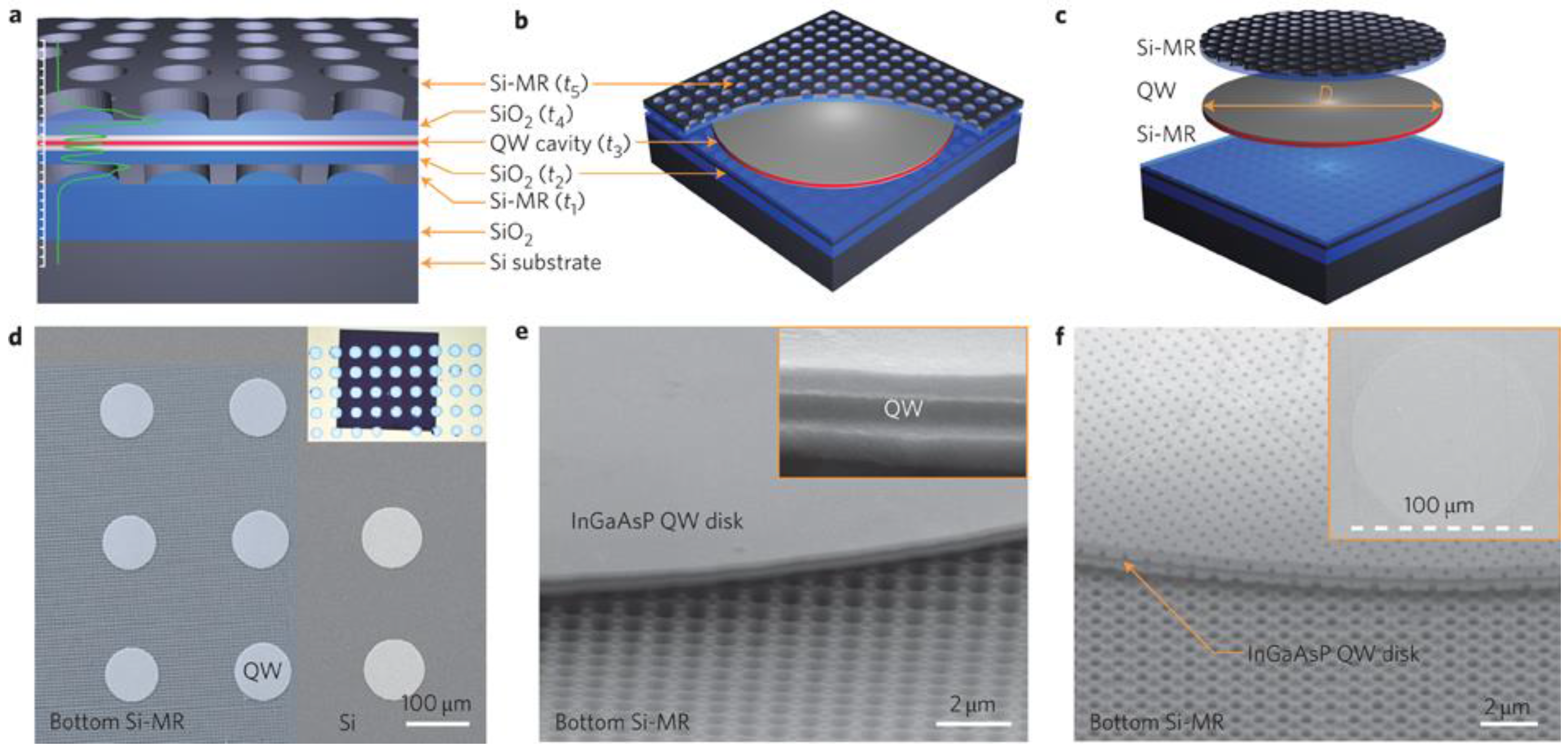
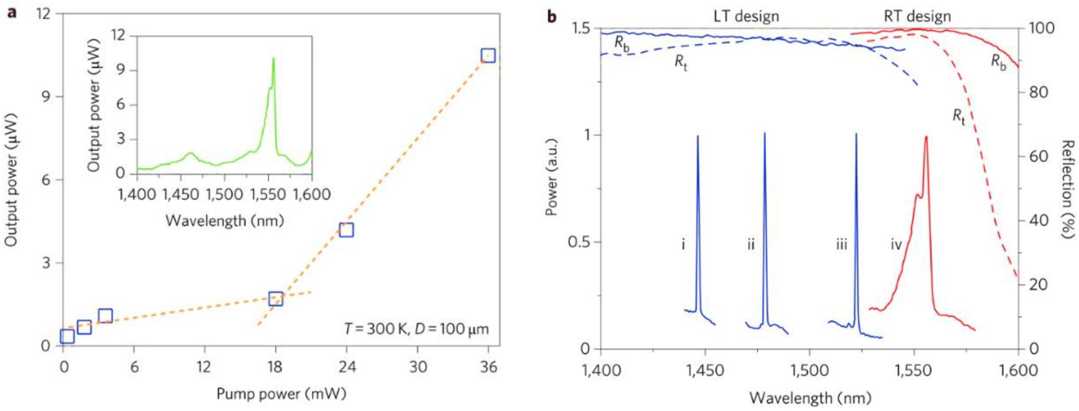
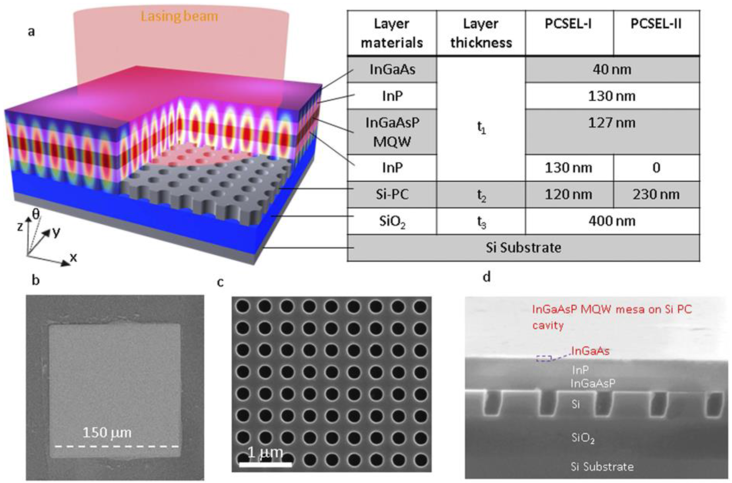
2.1.2. Photonic Crystal Surface-Emitting Laser
2.1.3. Edge-Emitting Lasers
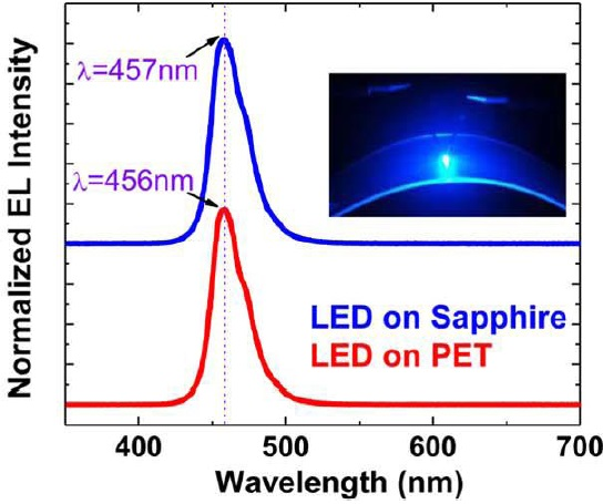
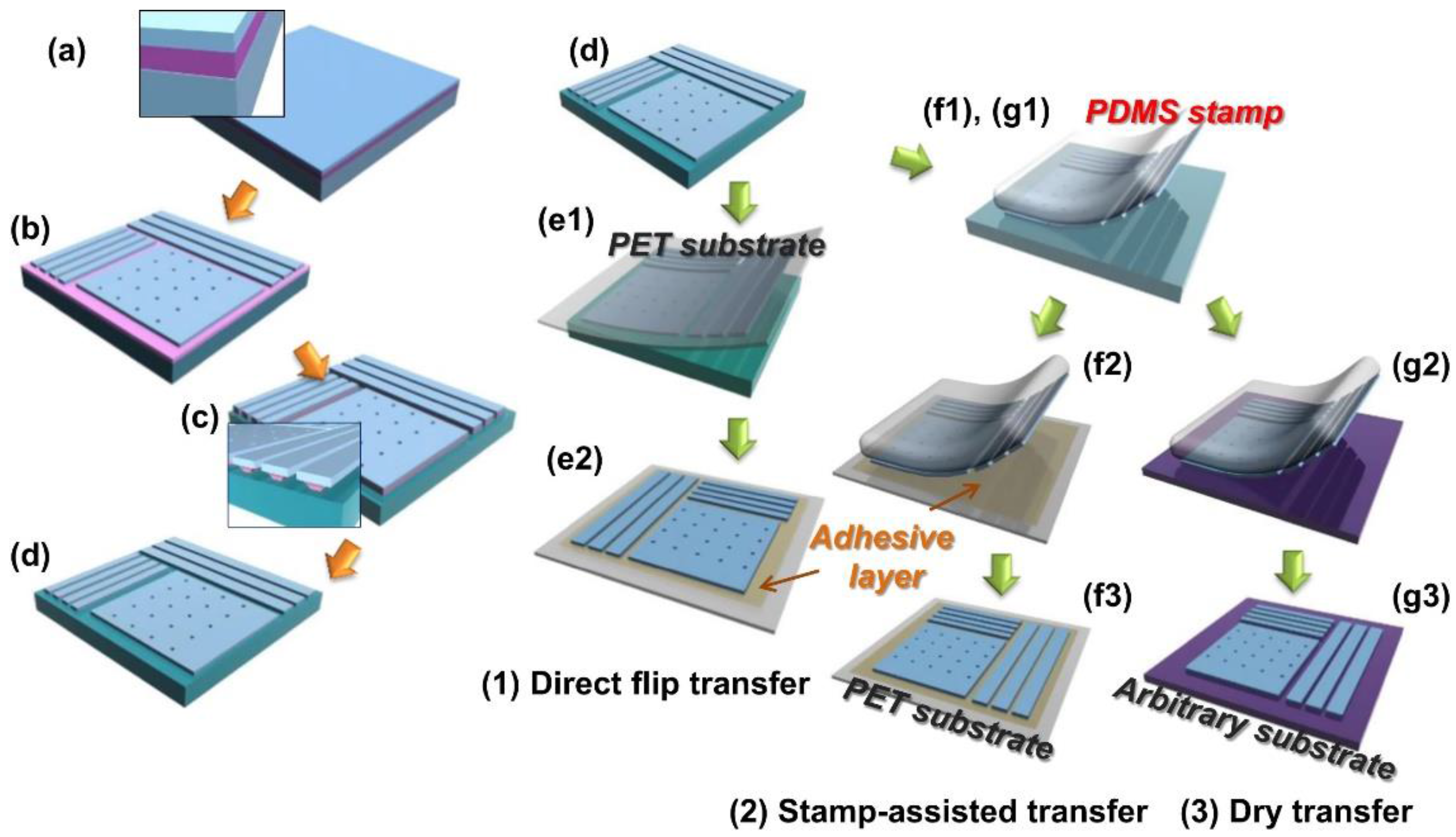
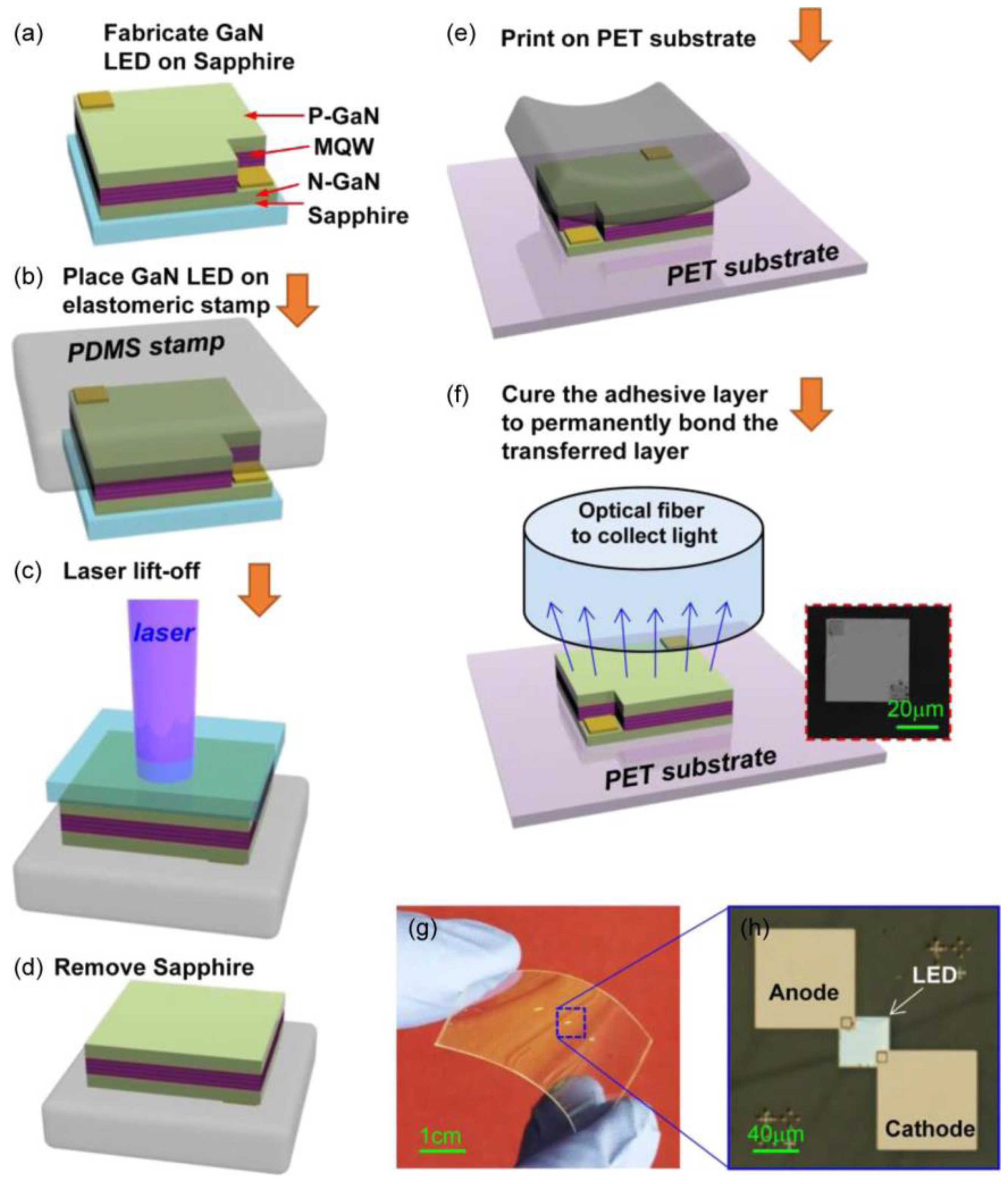
2.2. Flexible Light-Emitting Diode
3. Semiconductor Nanomembrane-Based Photodetecting Devices
3.1. Multi-Color Photodetector Arrays
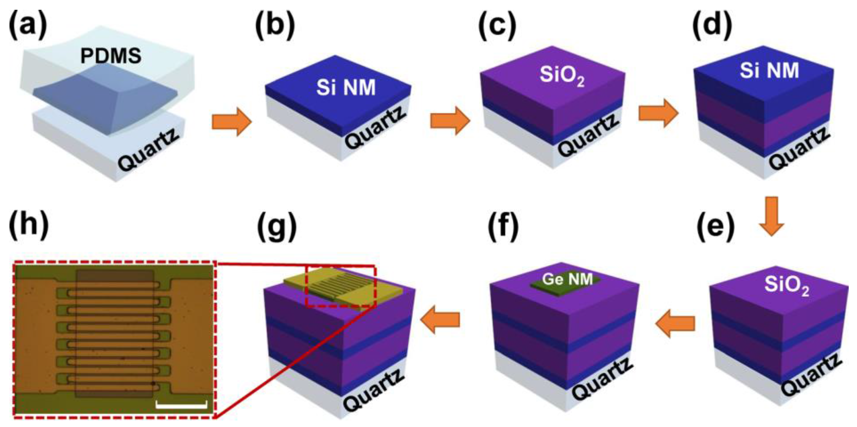
3.2. Germanium Photodetector with Enhanced Quantum Efficiency
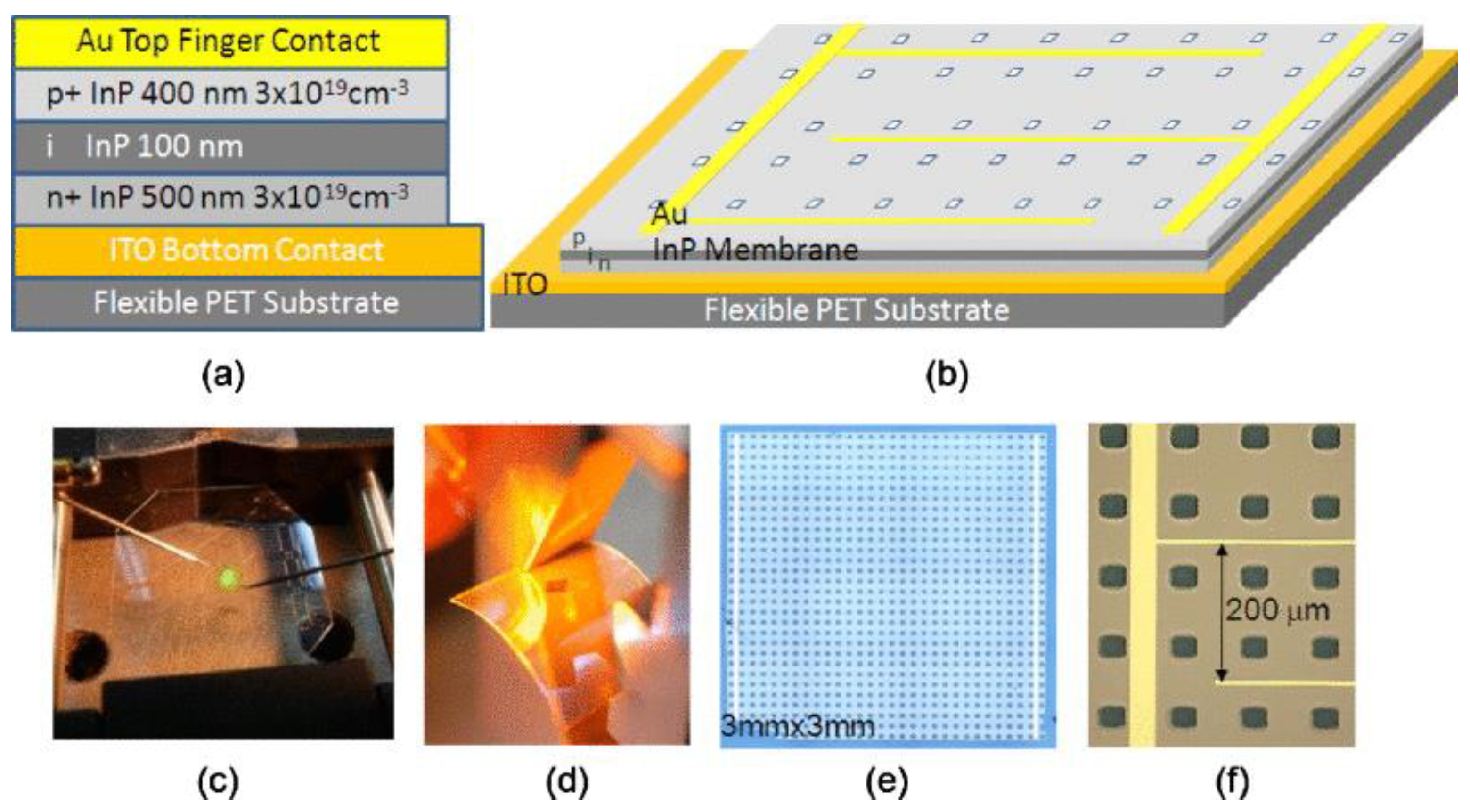
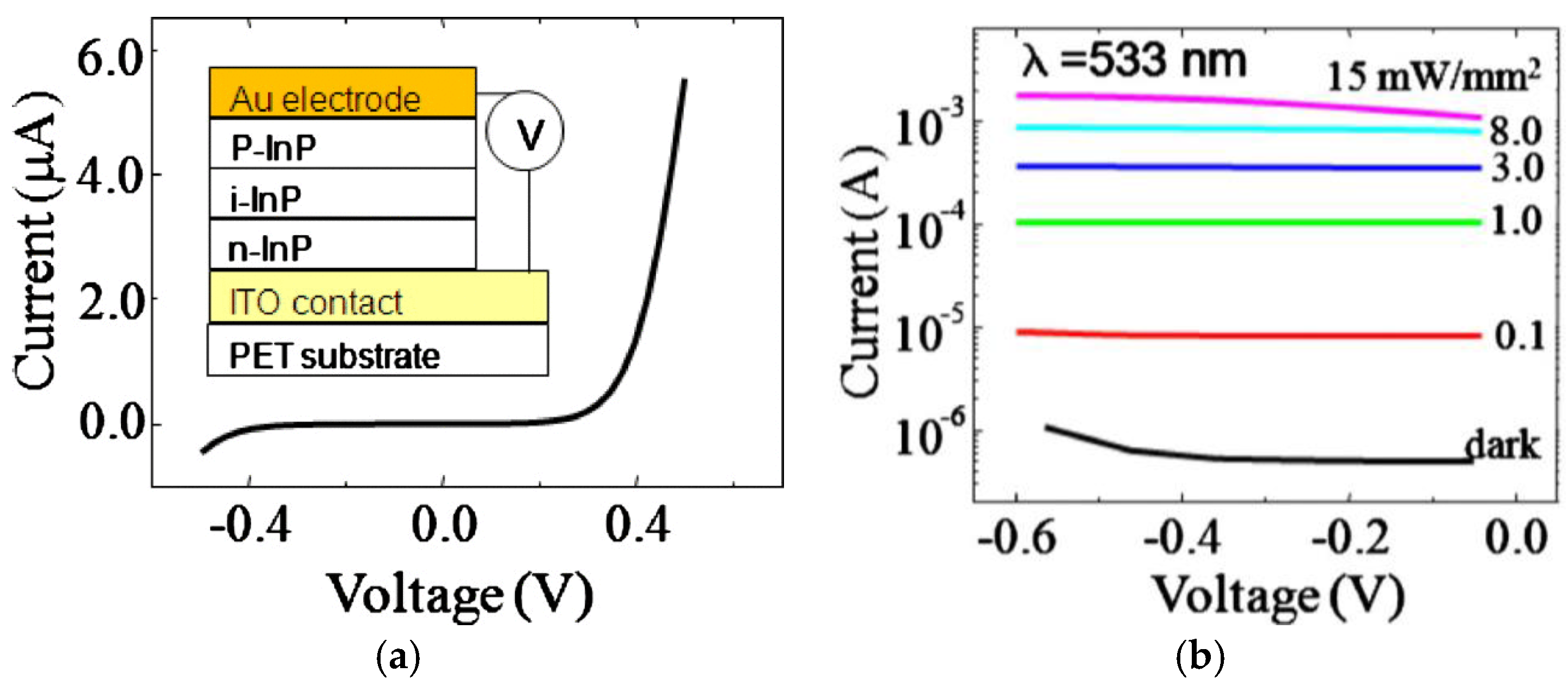
3.3. Large-Area InP NM-Based Flexible Photodetectors
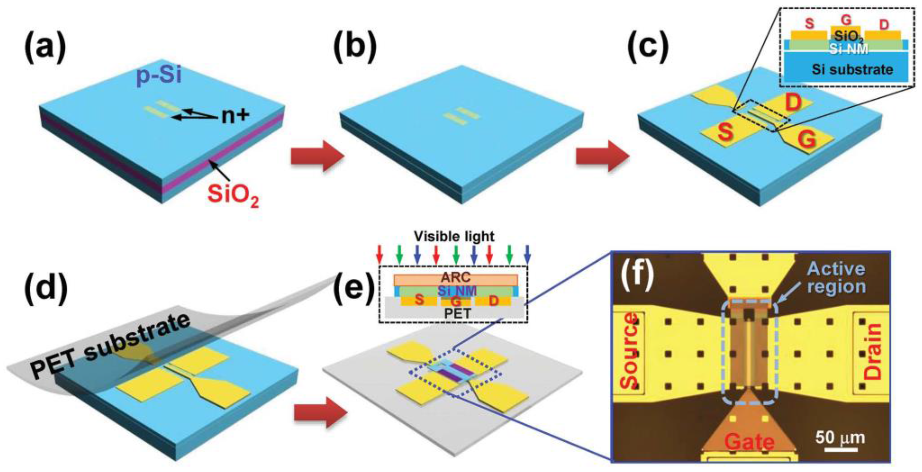
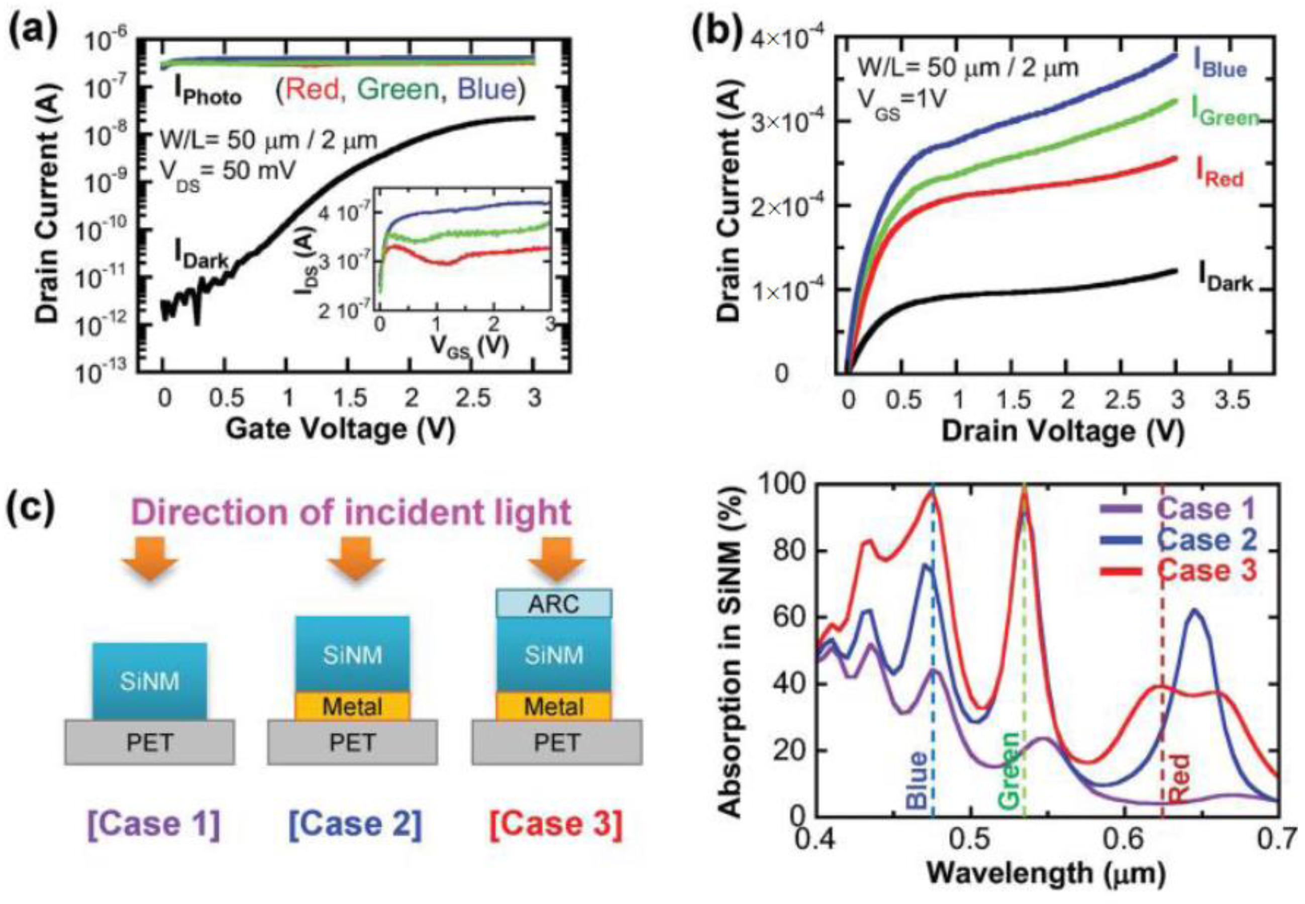
3.4. Silicon NM-Based Flexible Phototransistors
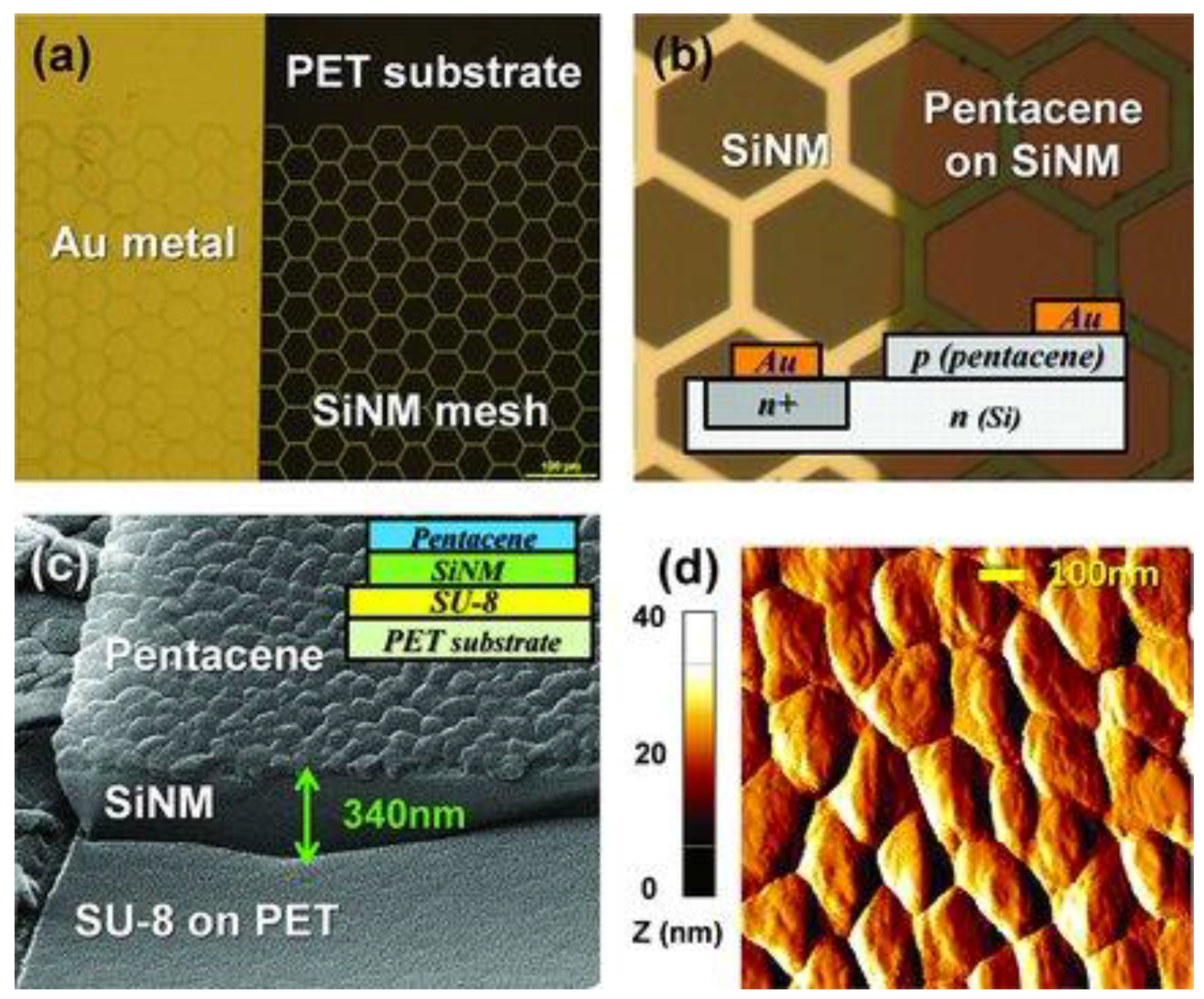
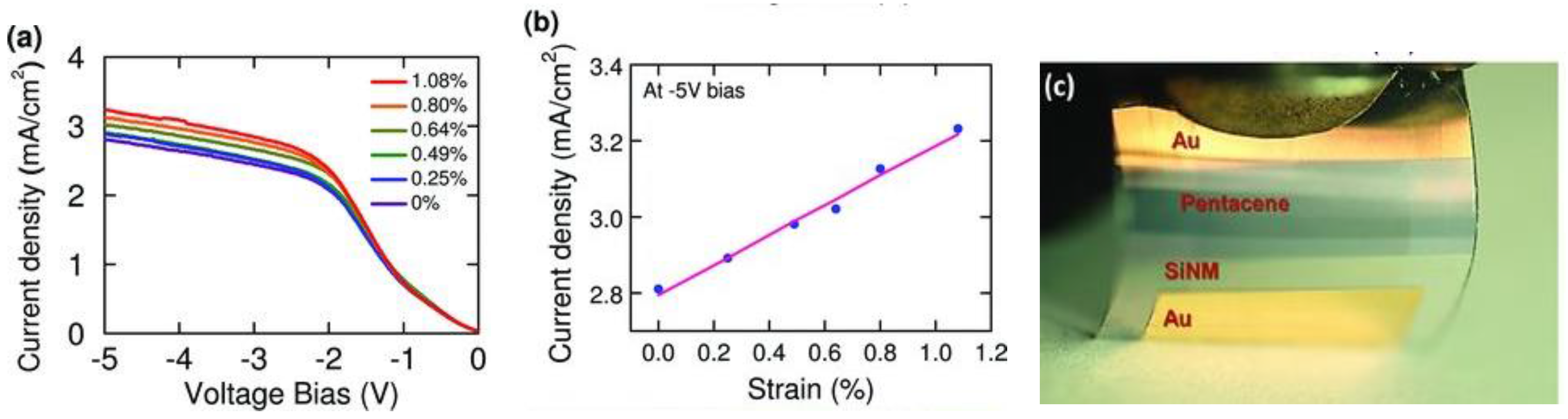
3.5. Flexible Photodetecting P-N Diode between Pentacene and Si NM
4. Conclusions and Outlooks
Acknowledgments
Conflicts of Interest
References
- Rogers, J.A.; Lagally, M.G.; Nuzzo, R.G. Synthesis, assembly and applications of semiconductor nanomembranes. Nature 2011, 477, 45–53. [Google Scholar] [CrossRef] [PubMed]
- Hwang, S.W.; Tao, H.; Kim, D.H.; Cheng, H.; Song, J.K.; Rill, E.; Brenckle, M.A.; Panilaitis, B.; Won, S.M.; Kim, Y.S.; et al. A physically transient form of silicon electronics. Science 2012, 337, 1640–1644. [Google Scholar] [CrossRef] [PubMed]
- Schmidt, O.G.; Eberl, K. Nanotechnology: Thin solid films roll up into nanotubes. Nature 2001, 410, 168. [Google Scholar] [CrossRef] [PubMed]
- Trotta, R.; Atkinson, P.; Plumhof, J.; Zallo, E.; Rezaev, R.; Kumar, S.; Baunack, S.; Schröter, J.; Rastelli, A.; Schmidt, O. Nanomembrane quantum light emitting diodes integrated onto piezoelectric actuators. Adv. Mater. 2012, 24, 2668–2672. [Google Scholar] [CrossRef] [PubMed]
- Li, X. Self-rolled-up microtube ring resonators: A review of geometrical and resonant properties. Adv. Opt. Photonic 2011, 3, 366–387. [Google Scholar] [CrossRef]
- Scott, S.A.; Lagally, M.G. Elastically strain-sharing nanomembranes: Flexible and transferable strained silicon and silicon-germanium alloys. J. Phys. D Appl. Phys. 2007, 40, R75–R92. [Google Scholar] [CrossRef]
- Yuan, H.C.; Ma, Z.; Roberts, M.M.; Savage, D.E.; Lagally, M.G. High-speed strained-single-crystal-silicon thin-film transistors on flexible polymers. J. Appl. Phys. 2006, 100. [Google Scholar] [CrossRef]
- Sun, L.; Qin, G.; Seo, J.H.; Celler, G.K.; Zhou, W.; Ma, Z. 12 GHz thin film transistors on transferrable silicon nanomembranes for high performance flexible electronics (cover story). Small 2010, 6, 2553–2557. [Google Scholar] [CrossRef] [PubMed]
- Zhang, K.; Seo, J.H.; Zhou, W.; Ma, Z. Fast flexible electronics using transferrable silicon nanomembranes (topical review). J. Phys. D Appl. Phys. 2012, 45. [Google Scholar] [CrossRef]
- Zhou, W.; Ma, Z.; Yang, H.; Qiang, Z.; Qin, G.; Pang, H.; Chen, L.; Yang, W.; Chuwongin, S.; Zhao, D. Flexible photonic-crystal fano filters based on transferred semiconductor nanomembranes. J. Phys. D Appl. Phys. 2009, 42. [Google Scholar] [CrossRef]
- Zhou, W.; Ma, Z.; Yang, H.; Chen, L.; Yang, W.; Qiang, Z.; Qin, G.; Pang, H.; Chuwongin, S.; Zhao, D. Semiconductor nanomembranes for stacked and flexible photonics. In Proceedings of the International Society for Optics and Photonics, San Francisco, CA, USA, 23 January 2010; p. 76060U.
- Yang, H.; Zhao, D.; Chuwongin, S.; Seo, J.H.; Yang, W.; Shuai, Y.; Berggren, J.; Hammar, M.; Ma, Z.; Zhou, W. Transfer-printed stacked nanomembrane lasers on silicon. Nat. Photonic 2012, 6, 615–620. [Google Scholar] [CrossRef]
- Zhou, H.; Seo, J.-H.; Paskiewicz, D.M.; Zhu, Y.; Celler, G.K.; Voyles, P.M.; Zhou, W.; Lagally, M.G.; Ma, Z. Fast flexible electronics with strained silicon nanomembranes. Sci. Rep. 2013, 3. [Google Scholar] [CrossRef] [PubMed]
- Meitl, M.A.; Zhu, Z.T.; Kumar, V.; Lee, K.J.; Feng, X.; Huang, Y.Y.; Adesida, I.; Nuzzo, R.G.; Rogers, J.A. Transfer printing by kinetic control of adhesion to an elastomeric stamp. Nat. Mater. 2006, 5, 33–38. [Google Scholar] [CrossRef]
- Harazim, S.M.; Quinones, V.A.B.; Kiravittaya, S.; Sanchez, S.; Schmidt, O. Lab-in-a-tube: On-chip integration of glass Optofluidic Ring Resonators for label-free Sensing Applications. Lab Chip 2012, 12, 2649–2655. [Google Scholar] [CrossRef] [PubMed]
- Song, Y.M.; Xie, Y.; Malyarchuk, V.; Xiao, J.; Jung, I.; Choi, K.-J.; Liu, Z.; Park, H.; Lu, C.; Kim, R.-H. Digital cameras with designs inspired by the arthropod eye. Nature 2013, 497, 95–99. [Google Scholar] [CrossRef] [PubMed]
- Zhou, W.; Ma, Z. Breakthroughs in nanomembranes and nanomembrane lasers. IEEE Photonic J. 2013, 5. [Google Scholar] [CrossRef]
- Zhou, W.; Zhao, D.; Shuai, Y.-C.; Yang, H.; Chuwongin, S.; Chadha, A.; Seo, J.-H.; Wang, K.X.; Liu, V.; Ma, Z. Progress in 2D photonic crystal Fano resonance photonics. Prog. Quantum Electron. 2014, 38, 1–74. [Google Scholar] [CrossRef]
- Hu, J.; Li, L.; Lin, H.; Zhang, P.; Zhou, W.; Ma, Z. Flexible integrated photonics: Where materials, mechanics and optics meet (invited). Opt. Mater. Express 2013, 3, 1313–1331. [Google Scholar] [CrossRef]
- Roberts, M.M.; Klein, L.J.; Savage, D.E.; Slinker, K.A.; Friesen, M.; Celler, G.; Eriksson, M.A.; Lagally, M.G. Elastically relaxed free-standing strained-silicon nanomembranes. Nat. Mater. 2006, 5, 388–393. [Google Scholar] [CrossRef] [PubMed]
- Rogers, J.A.; Someya, T.; Huang, Y. Materials and mechanics for stretchable electronics. Science 2010, 327, 1603–1607. [Google Scholar] [CrossRef] [PubMed]
- Janglin, C.; Liu, C.T. Technology advances in flexible displays and substrates. IEEE Access 2013, 1, 150–158. [Google Scholar] [CrossRef]
- Ko, H.; Takei, K.; Kapadia, R.; Chuang, S.; Fang, H.; Leu, P.W.; Ganapathi, K.; Plis, E.; Kim, H.S.; Chen, S.-Y. Ultrathin compound semiconductor on insulator layers for high-performance nanoscale transistors. Nature 2010, 468, 286–289. [Google Scholar] [CrossRef] [PubMed]
- Chen, Y.; Li, H.; Li, M. Flexible and tunable silicon photonic circuits on plastic substrates. Sci. Rep. 2012, 2. [Google Scholar] [CrossRef] [PubMed]
- Seo, J.H.; Zhang, K.; Kim, M.; Zhao, D.; Yang, H.; Zhou, W.; Ma, Z. Flexible phototransistors based on single-crystalline silicon nanomembranes. Adv. Opt. Mater. 2015, 4. [Google Scholar] [CrossRef]
- Seo, J.-H.; Zhang, Y.; Yuan, H.-C.; Wang, Y.; Zhou, W.; Ma, J.; Ma, Z.; Qin, G. Investigation of various mechanical bending strains on characteristics of flexible monocrystalline silicon nanomembrane diodes on a plastic substrate. Microelectron. Eng. 2013, 110, 40–43. [Google Scholar] [CrossRef]
- Gao, L.; Zhang, Y.; Malyarchuk, V.; Jia, L.; Jang, K.-I.; Webb, R.C.; Fu, H.; Shi, Y.; Zhou, G.; Shi, L. Epidermal photonic devices for quantitative imaging of temperature and thermal transport characteristics of the skin. Nat. Commun. 2014, 5. [Google Scholar] [CrossRef] [PubMed]
- Huang, C.C.; Wu, X.; Liu, H.; Aldalali, B.; Rogers, J.A.; Jiang, H. Large-field-of-view wide-spectrum artificial reflecting superposition compound eyes. Small 2014, 10, 3050–3057. [Google Scholar] [CrossRef] [PubMed]
- Xu, X.; Subbaraman, H.; Kwong, D.; Hosseini, A.; Zhang, Y.; Chen, R.T. Large area silicon nanomembrane photonic devices on unconventional substrates. IEEE Photonic Technol. Lett. 2013, 25, 1601–1604. [Google Scholar] [CrossRef]
- Zhao, D.; Liu, S.-C.; Yang, H.; Ma, Z.; Carl, R.-H.; Mattias, H.; Zhou, W. Printed Large-Area Single-Mode Photonic Crystal Bandedge Surface-Emitting Lasers on Silicon. Sci. Rep. 2016, 6, 18860. [Google Scholar] [CrossRef] [PubMed]
- Yang, H.; Zhao, D.; Liu, S.; Liu, Y.; Seo, J.-H.; Ma, Z.; Zhou, W. Transfer Printed Nanomembranes for Heterogeneously Integrated Membrane Photonics. Photonics 2015, 2, 1081–1100. [Google Scholar] [CrossRef]
- Xu, X.; Subbaraman, H.; Chakravarty, S.; Hosseini, A.; Lin, C.-Y.; Kwong, D.; Chen, R.T. Stamp printing of silicon-nanomembrane-based photonic devices onto flexible substrates with a suspended configuration. Opt. Lett. 2012, 37, 1020–1022. [Google Scholar] [CrossRef] [PubMed]
- Xu, X.; Subbaraman, H.; Chakravarty, S.; Hosseini, A.; Covey, J.; Yu, Y.; Chen, R.T. Flexible single-crystal silicon nanomembrane photonic crystal cavity. ACS Nano 2014, 8, 12265–12271. [Google Scholar] [CrossRef] [PubMed]
- Yang, H.; Zhao, D.; Seo, J.-H.; Chuwongin, S.; Kim, S.; Rogers, J.A.; Ma, Z.; Zhou, W. Broadband membrane reflectors on glass. IEEE Photonic Technol. Lett. 2012, 24, 476–478. [Google Scholar] [CrossRef]
- Yang, H.; Pang, H.; Qiang, Z.; Ma, Z.; Zhou, W. Surface-normal fano filters based on transferred silicon nanomembranes on glass substrates. Electron. Lett. 2008, 44, 858–859. [Google Scholar] [CrossRef]
- Qiang, Z.; Yang, H.; Chen, L.; Pang, H.; Ma, Z.; Zhou, W. Fano filters based on transferred silicon nanomembranes on unconventional substrates. IEEE Photonic Technol. Lett. 2013, 25, 1601–1604. [Google Scholar]
- Jung, Y.; Chang, T.-H.; Zhang, H.; Yao, C.; Zheng, Q.; Yang, V.; Mi, H.; Kim, M.; Cho, S.-J.; Park, D.-W.; et al. High-performance green flexible electronics based on biodegradable cellulose nanofibril paper. Nat. Commun. 2015, 6, 7170. [Google Scholar] [CrossRef] [PubMed]
- Justice, J.; Bower, C.; Meitl, M.; Mooney, M.; Gubbins, M.; Corbett, B. Wafer-scale integration of group III-V lasers on silicon using transfer printing of epitaxial layers. Nat. Photonic 2012, 6, 610–614. [Google Scholar] [CrossRef]
- Menon, L.; Yang, H.; Cho, S.-J.; Mikael, S.; Ma, Z.; Carl, R.-H.; Mattias, H.; Zhou, W. Heterogeneously Integrated InGaAs and Si Membrane Four-Color Photodetector Arrays. IEEE Photonics J. 2016, 8, 1–7. [Google Scholar] [CrossRef]
- Cho, M.; Seo, J.-H.; Kim, M.; Lee, J.; Liu, D.; Zhou, W.; Yu, Z.; Ma, Z. Resonant cavity germanium photodetector via stacked single-crystalline nanomembranes. JVSTB 2016, 34. [Google Scholar] [CrossRef]
- Yang, W.; Yang, H.; Qin, G.; Ma, Z.; Berggren, J.; Hammar, M.; Soref, R.; Zhou, W. Large-area InP-based crystalline nanomembrane flexible photodetectors. Appl. Phys. Lett. 2010, 96. [Google Scholar] [CrossRef]
- Seo, J.-H.; Oh, T.-Y.; Park, J.; Zhou, W.; Ju, B.-K.; Ma, Z. A Multifunction Heterojunction Formed between Pentacene and a Single-Crystal Silicon Nanomembrane. Adv. Funct. Mater. 2013, 23, 3398–3403. [Google Scholar] [CrossRef]
- Xia, Z.; Song, H.; Kim, M.; Zhou, M.; Chang, T.; Liu, D.; Xiong, K.; Yu, Z.; Ma, Z.; Gan, Q. Photodetecting MOSFET based on ultrathin single-crystal germanium nanomembrane. In Proceedings of Conference on Lasers and Electro-Optics: Science and Innovations 2016, San Jose, CA, USA, 5–10 June 2016.
- Seo, J.-H.; Li, J.; Lee, J.; Lin, J.; Jiang, H.; Ma, Z. A simplified method of making flexible blue LEDs on a plastic substrate. IEEE Photonic 2015, 7. [Google Scholar] [CrossRef]
- Chen, R.; Tran, T.-T.D.; Ng, K.; Ko, W.; Chuang, L.; Sedgwick, F.; Chang-Hasnain, C. Nanolasers grown on silicon. Nat. Photonic 2011, 5, 170–175. [Google Scholar] [CrossRef]
- Fang, A.W.; Cohen, O.; Jones, R.; Paniccia, M.J.; Bowers, J.E. Design and fabrication of optically pumped hybrid silicon-AlGaInAs evanescent lasers. IEEE J. Sel. Top. Quantum Electron. 2006, 12, 1657–1663. [Google Scholar]
- Fang, A.W.; Park, H.; Cohen, O.; Jones, R.; Paniccia, M.J.; Bowers, J.E. Electrically pumped hybrid AlGaInAs-silicon evanescent laser. Opt. Express 2006, 14, 9203–9210. [Google Scholar] [CrossRef] [PubMed]
- Vecchi, G.; Raineri, F.; Sagnes, I.; Yacomotti, A.; Monnier, P.; Karle, T.J.; Lee, K.-H.; Braive, R.; Gratiet, L.; Guilet, S.; et al. Continuous-wave operation of photonic band-edge laser near 1.55 μm on silicon wafer. Opt. Express 2007, 15, 7551–7556. [Google Scholar] [CrossRef] [PubMed]
- Hirose, K.; Liang, Y.; Kurosak, Y.; Watanabe, A.; Sugiyama, T.; Noda, S. Watt-class high-power, high-beam-quality photonic-crystal lasers. Nat. Photonic 2014, 8, 406–411. [Google Scholar] [CrossRef]
- Noda, S.; Yokoyama, M.; Imada, M.; Chutinan, A.; Mochizuki, M. Polarization mode control of two-dimensional photonic crystal laser by unit cell structure design. Science 2001, 293, 1123–1125. [Google Scholar] [CrossRef] [PubMed]
- Miyai, E.; Sakai, K.; Okano, T.; Kunishi, W.; Ohnishi, D.; Noda, S. Photonics: Lasers producing tailored beams. Nature 2006, 441, 946–946. [Google Scholar] [CrossRef] [PubMed]
- Dosunmu, O.I.; Cannon, D.D.; Emsley, M.K.; Ghyselen, B.; Liu, J.; Kimerling, L.C.; Unlu, M. Resonant Cavity Enhanced Ge Photodetectors for 1550 nm Operation on Reflecting Si Substrates. IEEE J. Sel. Top. Quantum Electron. 2004, 10, 694–701. [Google Scholar] [CrossRef]
- Tsagaris, V.; Anastassopoulos, V. Fusion of visible and infrared imagery for night color vision. Displays 2005, 26, 191–196. [Google Scholar] [CrossRef]
- Menon, L.; Yang, H.; Cho, S.; Mikael, S.; Ma, Z.; Zhou, W. Transferred flexible three-color silicon membrane photodetector arrays. IEEE Photonic J. 2015, 7, 1–6. [Google Scholar] [CrossRef]
- Michel, B.; Bernard, A.; Andre-Jacques, A.-H. Smart-Cut: A New Silicon on Insulator Material Technology Based on Hydrogen Implantation and Wafer Bonding. Jpn. J. Appl. Phys. 1997, 36, 1636–1641. [Google Scholar]
- Chen, L.; Qiang, Z.; Yang, H.; Pang, H.; Ma, Z.; Zhou, W. Polarization and angular dependent transmissions on transferred nanomembrane Fano filters. Opt. Express 2009, 17, 8396–8406. [Google Scholar] [CrossRef] [PubMed]
- Hamilton, M.C.; Martin, S.; Kanicki, J. Thin-Film Organic Polymer Phototransistors. IEEE Trans. Electron. Devices 2004, 51, 877–885. [Google Scholar] [CrossRef]
- Cheng, H.L.; Liang, X.W.; Chou, W.Y.; Mai, Y.S.; Yang, C.Y.; Chang, L.R.; Tang, F.C. Raman spectroscopy applied to reveal polycrystalline grain structures and carrier transport properties of organic semiconductor films: Application to pentacene-based organic transistors. Org. Electron. 2009, 10, 289–298. [Google Scholar] [CrossRef]
- Cheng, H.L.; Chou, W.Y.; Kuo, C.W.; Tang, F.C.; Wang, Y.W. Electric field-induced structural changes in pentacene-based organic thin-film transistors studied by in situ micro-Raman spectroscopy. Appl. Phys. Lett. 2006, 88. [Google Scholar] [CrossRef]
- Peng, C.-Y.; Huang, C.-F.; Fu, Y.-C.; Yang, Y.-H.; Lai, C.-Y.; Chang, S.-T.; Liu, C.W. Comprehensive study of the Raman shifts of strained silicon and germanium. J. Appl. Phys. 2009, 105. [Google Scholar] [CrossRef]


© 2016 by the authors; licensee MDPI, Basel, Switzerland. This article is an open access article distributed under the terms and conditions of the Creative Commons Attribution (CC-BY) license (http://creativecommons.org/licenses/by/4.0/).
Share and Cite
Liu, D.; Zhou, W.; Ma, Z. Semiconductor Nanomembrane-Based Light-Emitting and Photodetecting Devices. Photonics 2016, 3, 40. https://doi.org/10.3390/photonics3020040
Liu D, Zhou W, Ma Z. Semiconductor Nanomembrane-Based Light-Emitting and Photodetecting Devices. Photonics. 2016; 3(2):40. https://doi.org/10.3390/photonics3020040
Chicago/Turabian StyleLiu, Dong, Weidong Zhou, and Zhenqiang Ma. 2016. "Semiconductor Nanomembrane-Based Light-Emitting and Photodetecting Devices" Photonics 3, no. 2: 40. https://doi.org/10.3390/photonics3020040