1. Introduction
Photonic integration endeavors to bring multiple optical functions into a compact device with a small footprint, low power consumption and reliable performance, analogous to electronic integration. However, contrary to the situation in the electronic industry where silicon CMOS dominates, photonic devices nowadays do not tend to converge to one major material system. Light sources are mostly realized using III-V semiconductor-related materials. Modulators have been dominated by lithium niobate (LiNbO3), but have been gradually taken over by InP and silicon-on-insulator (SOI) platforms. Detectors are fabricated using III-V semiconductors and Si-Ge materials. Waveguide networks, filters, and other passive optical functions can be realized in low-cost platforms such as polymer, silica and silicon nitride planar lightwave circuits (PLCs). Hybrid photonic integration allows for selecting individual components from the respective best-suited material platform and for assembling them in a common motherboard. These components can be tested prior to the assembly. In this way, high freedom of device performance and yield optimization can be realized, leading to a relatively high cost-efficiency. With the help of the automatic alignment tools and machine-assisted assembly equipment, hybrid integration can offer the benefits of micro-optical packaging at reduced costs, potentially higher overall module performance and higher reliability. Its versatility makes it particularly useful for low to medium production volumes.
In the last decade, polymer-based photonic devices and the hybrid integration platform have witnessed significant advancement [
1,
2,
3]. Multi-core polymer waveguides and multi-step 45° mirror arrays have been fabricated as a bridging devices toward spatial-division-multiplexed (SDM) transmission systems [
4,
5,
6]. Silicon nitride (SiN
x) has been introduced as high-index core material and related thermo-optic devices have been reported [
7,
8,
9,
10]. Polymer arrayed waveguide gratings (AWGs) coupled with 40-channel laser diodes (LDs) and photo detectors (PDs) have been implemented as optical line terminals (OLTs) in the wavelength-division-multiplexed passive optical network (WDM-PON) [
11,
12]. Clever arrangement of thermally tunable Bragg gratings, vertically inserted thin-film element (TFE), on-chip U-groove and 45° mirror has led to the assembly of a compact, bi-directional optical network unit (ONU) [
13]. Ultrafast electro-optic polymer modulators, integrated with InP-based light sources and driver electronics, have been packaged into transmitter modules, providing serial 100 Gb/s connectivity in data centers and metro-area optical networks [
14,
15,
16,
17,
18,
19].
In this work, a review is performed summarizing the latest development of the polyboard technology. From waveguides to optical assemblies and finally to packaged modules, details of the heterogeneous/ hybrid integration technology are revealed, uncovering the integration flexibility, scalability, and cost-effectiveness this platform offers. Moreover, functionalities such as wavelength tunability and polarization control can be realized in a simple and clean manner, making this platform highly attractive in applications where colorless and polarization-multiplexed operations are required.
2. Polymer Waveguides
Both ridge waveguides and channel waveguides can be fabricated on polymer platforms. The square-shaped core of a channel waveguide can be adopted to minimize the waveguide birefringence. The refractive index can be chosen from ~1.4 to ~1.7, depending on the chemical composition. The dimension of the core measures a few micrometers for single mode operation. Optical polymer layers can be formed by spin-coating and subsequent UV and temperature curing. Silicon wafers are usually taken as substrate, though the technology is also applicable on glass plates, ceramic and InP wafers. The structuring of the waveguide follows mainly three methods [
20]: (1) standard semiconductor processing methods with photolithography and reactive ion etching; (2) direct UV lithographic patterning followed by wet-chemical rinsing; and (3) soft molding and imprinting. In this work, the first fabrication method has been used. The technology details have been published in [
2,
5,
7]. Metals can be inserted virtually anywhere in the vicinity of the waveguide to function as heater electrodes for thermally tunable devices but also as RF electrodes to drive the electro-optic (EO) polymer-based modulator.
The fabrication process can be repeated to stack up the polymer waveguide layers into a multi-core structure [
5], as shown in
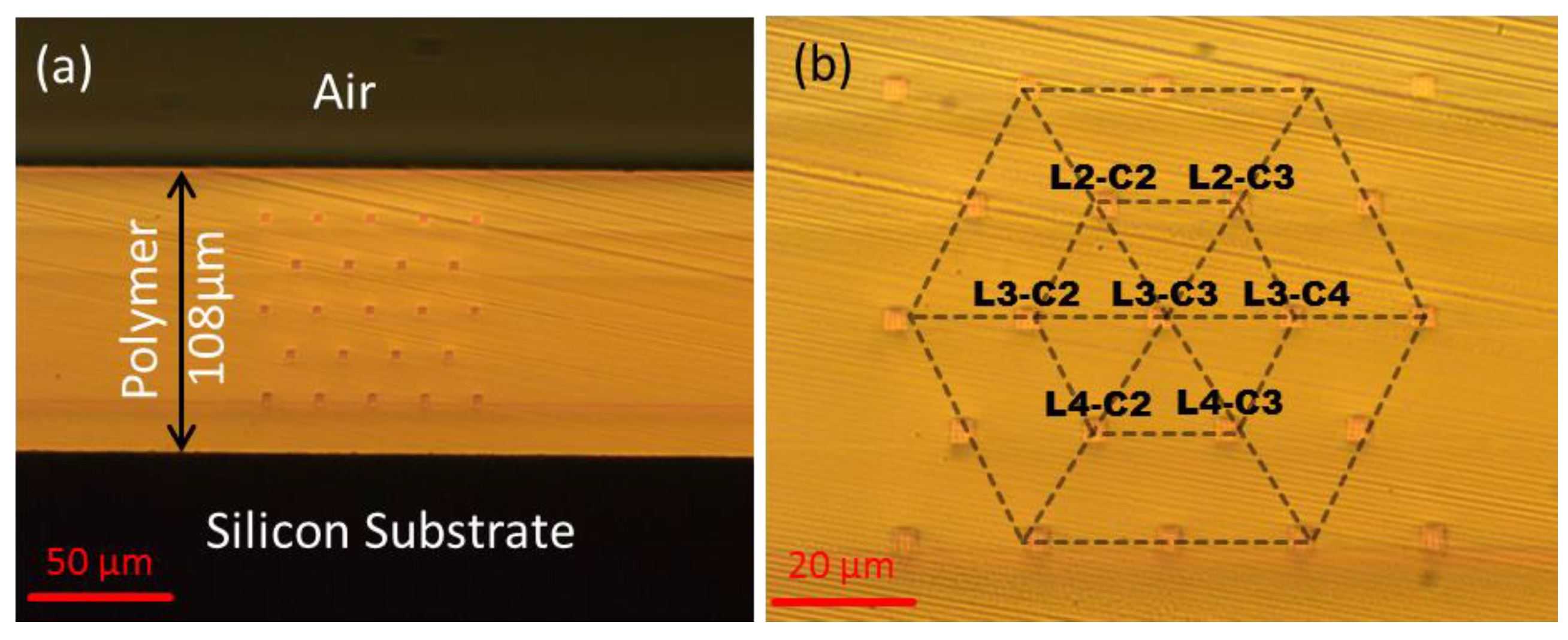
Figure 1a,b. The waveguide features a square-core of 3 µm × 3 µm and a core/cladding index contrast of 1.48/1.45. A bending radius of 1.5 mm of such a waveguide will lead to a loss ~0.12 dB for a 90° bend. The five-layer polymer waveguides shown in
Figure 1a add up to a total thickness of 108 µm, within which the bottom cladding is 20 µm directly above the silicon substrate, the inter-waveguide-layer distance is 17.32 µm (4 times), and the upper cladding is 15.7 µm below air. The waveguide loss among all five layers is below 1 dB/cm and the crosstalk between the waveguides at the 20-µm hexagonal lattice is below −40 dB after a propagation distance of 3.8 cm. This technology can be exploited to fabricate three-dimensional photonic integrated circuits (PICs) with high vertical density.
On a polymer platform, 45° facets can be created by applying a fast-rotating angled dicing blade and sawing through the polymer chip [
2]. The surface roughness can be minimized by the intrinsic “polishing” during sawing. The high concentration of small diamond grains on the blade tip, fast rotation speed and slow feeding speed can help generate a smooth surface. To improve the reflectivity, the 45° surface should be coated with a thin layer of metal, typically Ti and Au, by directed metal evaporation. Apart from the design and processing simplicity, such 45° deflection mirrors offer much broader coupling bandwidth, less polarization sensitivity, and less beam divergence, when compared to the vertical grating couplers. The 45° groove is usually filled with index matching epoxy so that the back reflection on the straight facet can be suppressed and the beam divergence in the free space can be reduced.
Figure 1.
Microscope images of the five-layer multi-core polymer waveguides, illuminated through the cross-section. (a) Broader view showing the total thickness of the polymer layers on silicon substrate and (b) detailed view showing the alignment of the waveguides on the 20-µm hexagonal lattice.
Figure 1.
Microscope images of the five-layer multi-core polymer waveguides, illuminated through the cross-section. (a) Broader view showing the total thickness of the polymer layers on silicon substrate and (b) detailed view showing the alignment of the waveguides on the 20-µm hexagonal lattice.
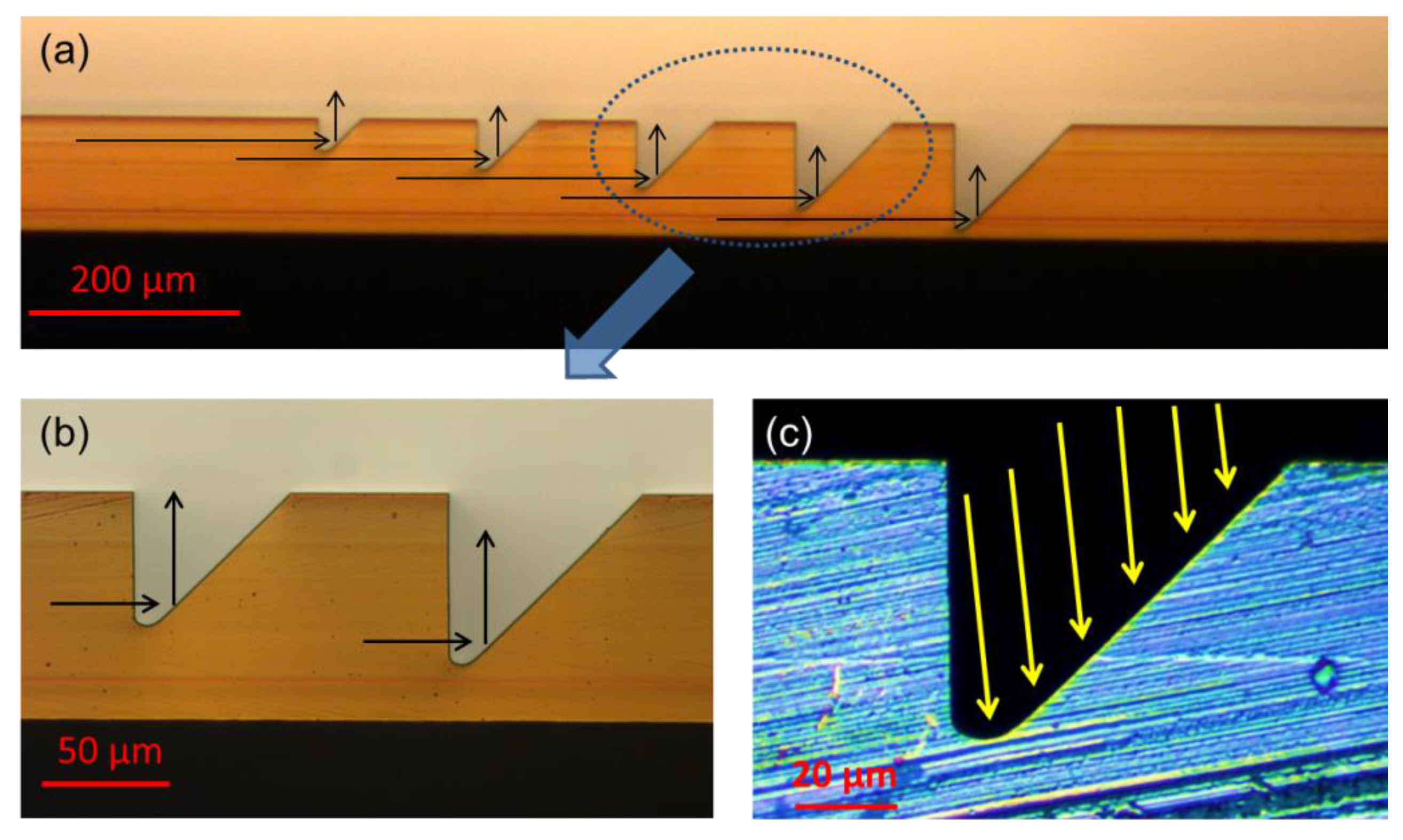
The 45° mirrors can be arrayed by varying the dicing depths to tap out light from each of the multi-layer waveguide cores separately, as indicated in
Figure 2. The depth of the mirrors must be calculated and well controlled so that the tip reaches, in the ideal case, the middle point between the two core layers. Light from each layer can then be subsequently extracted by the mirror array. To ensure that the metal coating reaches the very bottom of the deep mirror, while staying clear from the straight waveguide facet, thermal evaporation with well-defined deposition directivity must be used. The tilt angle must be carefully calculated. The waveguides can fan out with a larger in-plane pitch and the lateral distance between the mirrors can be adjusted to allow the attachment of either separate 1D planar PD bars or a common 2D PD array. The attachment can be done passively and automatically by a pick-and-placer. No extra submount is needed for the backside illuminated PDs.
Figure 2.
Microscope images of the five-step 45° mirrors. (a) Broader view and (b) detailed view showing the placement of the mirrors with backside illumination through the polymer, before the mirror surface metallization. (c) Detailed view illuminated from the top, revealing the metalized surface. The yellow arrows indicate the 10° angle in which the metal vapor is applied.
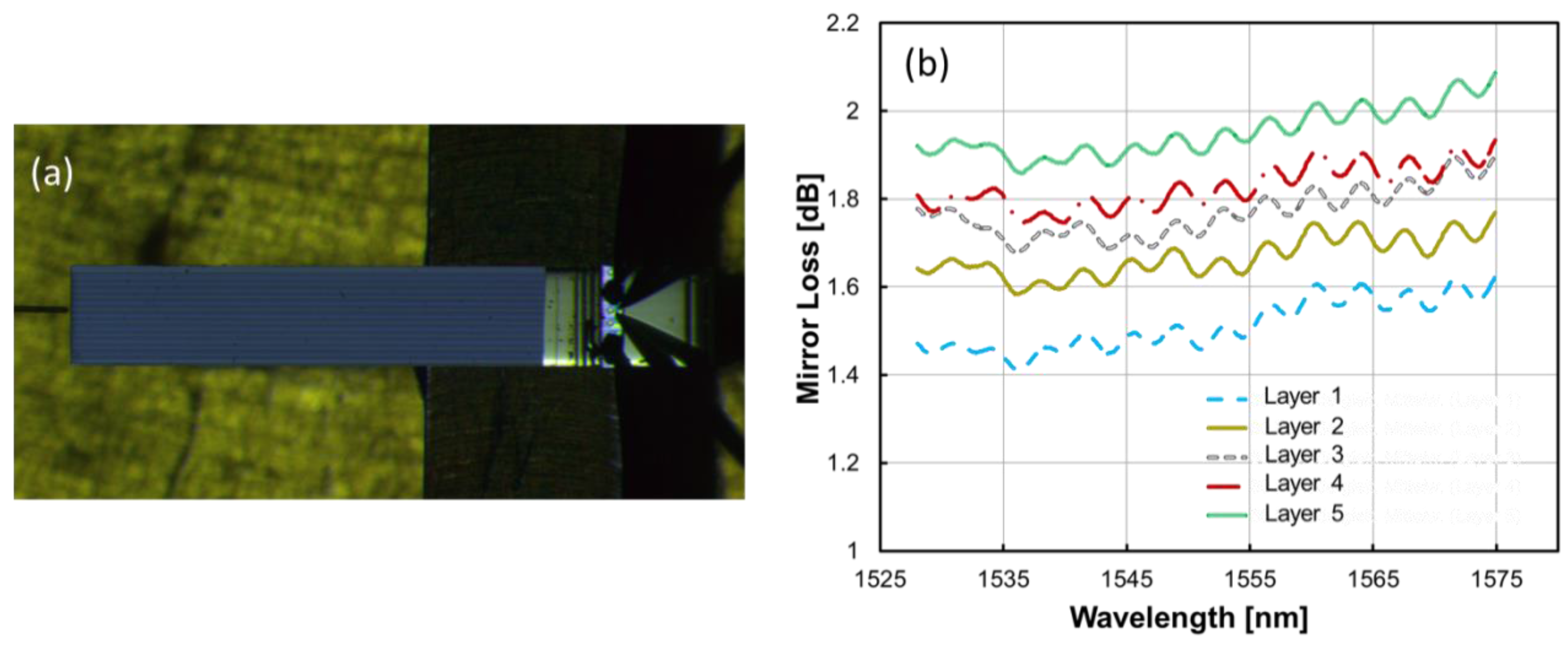
For testing of the mirrors, a tunable laser source is launched via a lensed fiber into the 1-cm long multicore waveguide chip and collected from the corresponding mirrors by a PD bar. The measurement setup is shown in
Figure 3a. Index matching oil is used to fill the mirror groove to limit the beam divergence as well as to reduce the back reflection at the PD surface. The multi-step mirror losses are displayed in
Figure 3b, ranging from 1.5 dB to 1.9 dB at 1550 nm. The bottom mirrors suffer gradually more losses, caused by the longer free-space beam propagation and associated larger beam divergence, scattering, and more material absorption in the oil filled region. The mirror loss can be further reduced by applying proper waveguide tapers to limit the beam divergence and by optimizing the dicing parameters for a smoother mirror surface.
Figure 3.
(a) Photograph of the 1-cm long multilayer waveguides and multi-step mirrors under test. Optical input (left): lensed fiber; electrical output (right): planar PD bar with probe contacts. (b) Mirror loss from each waveguide layer extracted from the PD responsivity.
Figure 3.
(a) Photograph of the 1-cm long multilayer waveguides and multi-step mirrors under test. Optical input (left): lensed fiber; electrical output (right): planar PD bar with probe contacts. (b) Mirror loss from each waveguide layer extracted from the PD responsivity.
To increase the waveguide index contrast and bring down the device footprint, amorphous silicon nitride (SiN
x) can be deposited on the polymer cladding by plasma enhanced chemical vapor deposition (PECVD) up to 300 °C [
7,
8,
9,
10]. The SiN
x / polymer heterogeneous waveguides can then be created. The aspect ratio of the SiN
x core can be adjusted to tailor the mode field diameter. For a thickness below 200 nm and a width of a few micrometers, the majority of the mode resides in the cladding and the waveguide loss depends primarily on the polymer material absorption. The minimal bending radius is 1 mm. The large aspect ratio often causes strong waveguide birefringence. Nevertheless, propagation loss below 1 dB/cm has been demonstrated for both polarizations [
7].
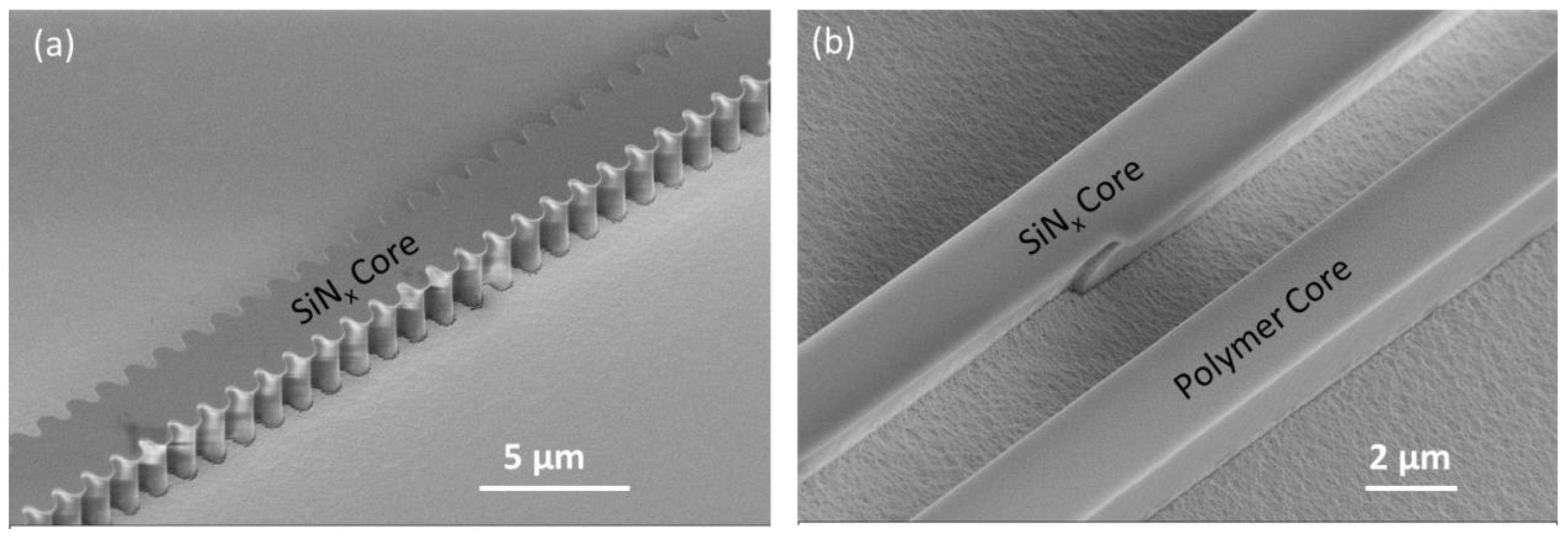
The strong thermo-optic effect of the polymer material (coefficient ranging from −1 × 10
−4 K
−1 to −3 × 10
−4 K
−1) can be utilized for such waveguides. Gratings can be created along the SiN
x core, as shown in
Figure 4a. Tunable Bragg reflectors and sampled grating filters have hence been demonstrated [
7,
8,
9]. Further developed is a grating-assisted co-directional coupler consisting of two parallel asymmetric waveguides, one with SiN
x core and the other with polymer core [
10]. The SEM photo of the coupler is shown in
Figure 4b. Long-period gratings are formed along the SiN
x waveguide for phase matching and wavelength filtering. The coupler is differentially thermally tunable. The temperature gradient distribution, introduced by a pair of offset micro-heaters, can either red or blue-shift the filter curve, depending on which waveguide appears “hotter”. A total tuning range of 82 nm is demonstrated experimentally.
Figure 4.
(a) SEM photo of a SiNx waveguide Bragg grating and (b) SEM photo of a SiNx/Polymer grating assisted coupler. Both photos are taken before the polymer top cladding is spin-coated.
Figure 4.
(a) SEM photo of a SiNx waveguide Bragg grating and (b) SEM photo of a SiNx/Polymer grating assisted coupler. Both photos are taken before the polymer top cladding is spin-coated.
Such waveguides have the potential to substantially enhance the versatility of polymer-based waveguide platforms. Higher contrast waveguides are feasible by using alternative materials, such as amorphous silicon with similar PECVD technology or sputtered TiO2 and Ta2O5 films. Compared to the all-polymer waveguides that require at least two compatible polymeric materials with well-adjusted refractive indices, a wider choice of useful polymers can be considered, e.g., aiming at lower material absorption, larger thermo-optical coefficients and higher thermal stability.
The multi-layer and heterogeneous waveguide technology can well be combined to construct a powerful waveguide platform that can incorporate a variety of organic and inorganic materials to build, layer by layer, complex 3D PICs. High-index dielectrics can be adopted to shrink down the size of the waveguide components and the lattice can be made much more compact without severe crosstalk. Metals can be imbedded as local heaters and RF interconnects. The polymer cladding serves as an immersive motherboard, supporting the overall infrastructure and providing flexible I/Os with multi-depth fiber grooves, slots and 45° mirror arrays.
3. Polymer AWG-Based OLTs
Optical line terminals (OLTs) and optical network units (ONU) are basic building blocks in the WDM-PON infrastructure. The hybrid integration approach allows high-performance and cost-effective OLTs to be assembled using polymer arrayed waveguide gratings (AWGs) for wavelength multiplexing (MUX) and de-multiplexing (DMX). InP LD arrays can be direct modulated as transmitters (Tx) and planar PD arrays function as high speed receivers (Rx).
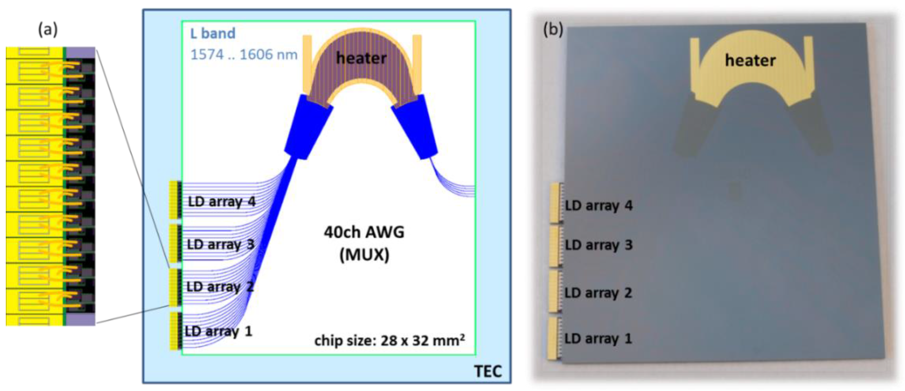
On the transmitter side, the OLT-Tx is shown in
Figure 5a,b. This device consists of four InP-based 10-chanel DFB LD arrays first placed on a Si submount and then butt-joint coupled to a polymer MUX AWG. The complete device, combining the AWG and the LD arrays, is 29 mm long and 30 mm wide. The 40-channel MUX AWG is based on a polymer waveguide with square cross-section of 3.5 μm × 3.5 μm and a refractive index contrast of 1.47/1.45. It is designed to cover the L-band (1574.4 nm–1606.4 nm) with 100 GHz channel spacing. The spectral characteristic of the AWG channels is of Gaussian type with a 1-dB bandwidth of 0.25 nm. The temperature dependence is ~0.04 nm/°C. A heater electrode placed on top of the arrayed waveguide region can be biased to thermally adjust the AWG central wavelengths to match the ITU-grids [
11].
Figure 5.
40-channel OLT-Tx based on 4 × 10 direct modulated LD arrays butt-joint coupled to a thermally tunable polymer AWG. (a) The schematic layout and (b) photograph of the assembly.
Figure 5.
40-channel OLT-Tx based on 4 × 10 direct modulated LD arrays butt-joint coupled to a thermally tunable polymer AWG. (a) The schematic layout and (b) photograph of the assembly.
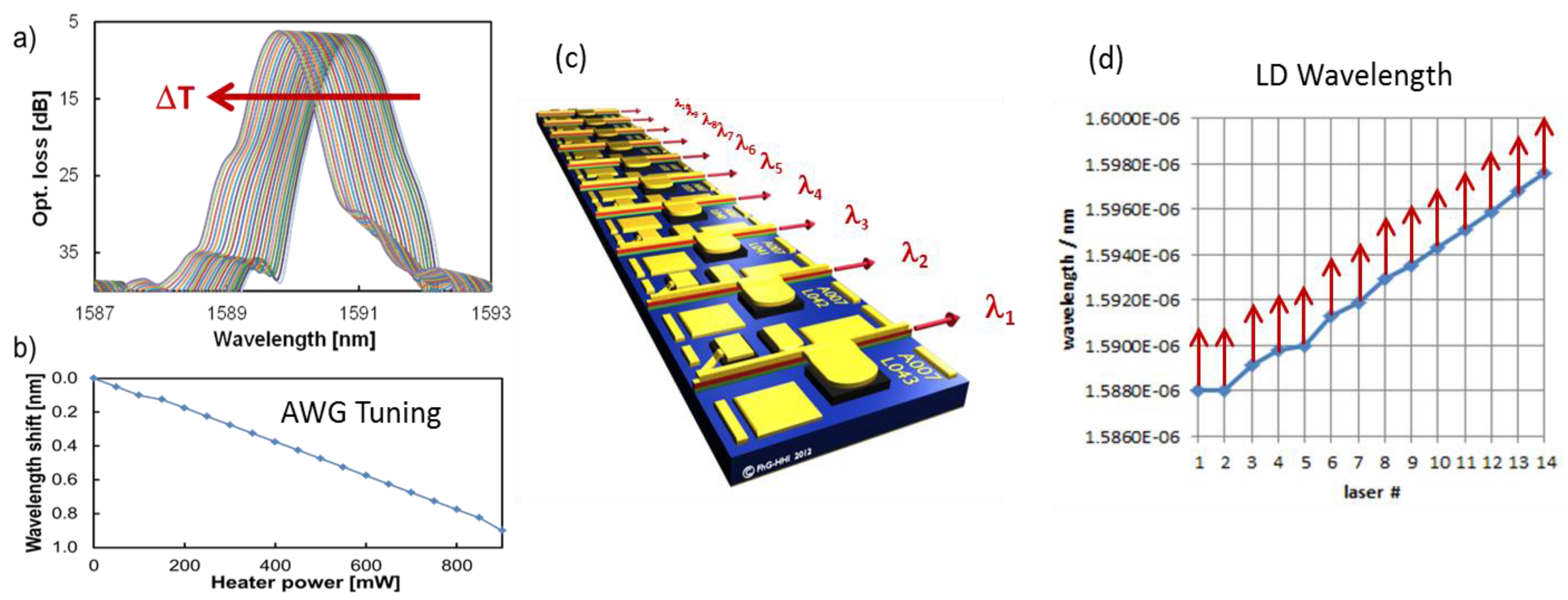
Figure 6.
(a) Overlaid AWG spectra at different heater powers; (b) AWG central wavelength during thermal tuning; (c) schematic layout of the multi-wavelength LD array; (d) the measured emission wavelengths.
Figure 6.
(a) Overlaid AWG spectra at different heater powers; (b) AWG central wavelength during thermal tuning; (c) schematic layout of the multi-wavelength LD array; (d) the measured emission wavelengths.
Figure 6a shows the overlaid spectra of the AWG at different heater powers.
Figure 6b exacts and plots the central wavelength during the thermal tuning. At ~900 mW, the tuning range exceeds the channel spacing of ~0.8 nm. The schematic layout of the InP LD array is shown in
Figure 6c. Each single element comprises a 150-µm-long DFB section and a 250-µm-long extra amplification section to increase the front side optical output power. The emission wavelength for each individual LD is defined by the e-beam lithography to set the 100-GHz channel spacing. A heater electrode is included in the DFB section and up to 3-nm tuning can be realized thermally, in order to pin-point the wavelengths at the ITU grid. The emitting wavelengths of different LDs on the array are listed in
Figure 6d. The 4 × 10-channel LD arrays construct the 40 defined channels in the L-band. The LD arrays are first mounted on the Si-submounts with pre-defined RF lines and then butt-joint coupled to the polymer-based AWG. The arrays have been high-reflection (HR) coated on the back side against air, whereas the front facet has an anti-reflection (AR) coating against polymer to avoid back reflections. Index-matching epoxy is first applied to secure the optical coupling, followed by a mechanical fixing epoxy to support the large array.
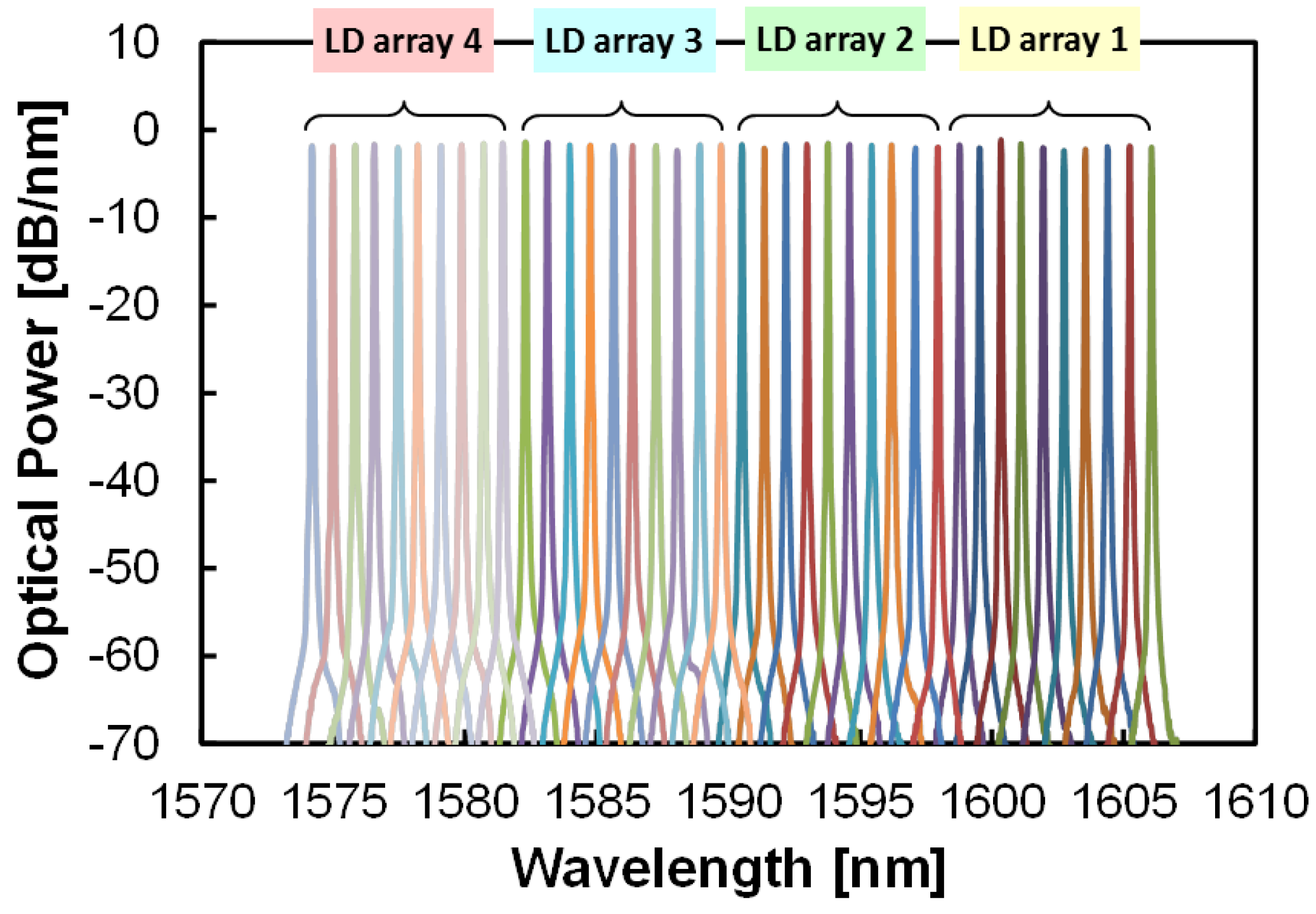
The assembled OLT-Tx is placed on the thermo-electric cooler (TEC), which stabilizes the assembly temperature at 25 °C. The performance is evaluated and displayed in
Figure 7, where the spectra of the 40 channels are measured at the outputs of the MUX AWG. An optical power larger than 0 dBm has been obtained in the fiber at a drive current ~120 mA. The spectrum of the AWG is firstly adjusted to match the central wavelengths defined by the ITU-Grid. The emitting wavelengths of the individual LDs are then aligned to the grid. The coinciding spectra from the AWG and the LDs lead to a stunningly sharp wavelength response and the achieved side mode suppression ratio (SMSR) exceeds 70 dB for all the 40 channels. With LDs (EMLs) that can be direct modulated faster than 25 Gb/s [
21], a total bit rate larger than 1 Tb/s can be achieved for this type of OLT-Tx device.
Figure 7.
Multiplexed transmission spectra at the output of the OLT-Tx (measured in fiber).
Figure 7.
Multiplexed transmission spectra at the output of the OLT-Tx (measured in fiber).
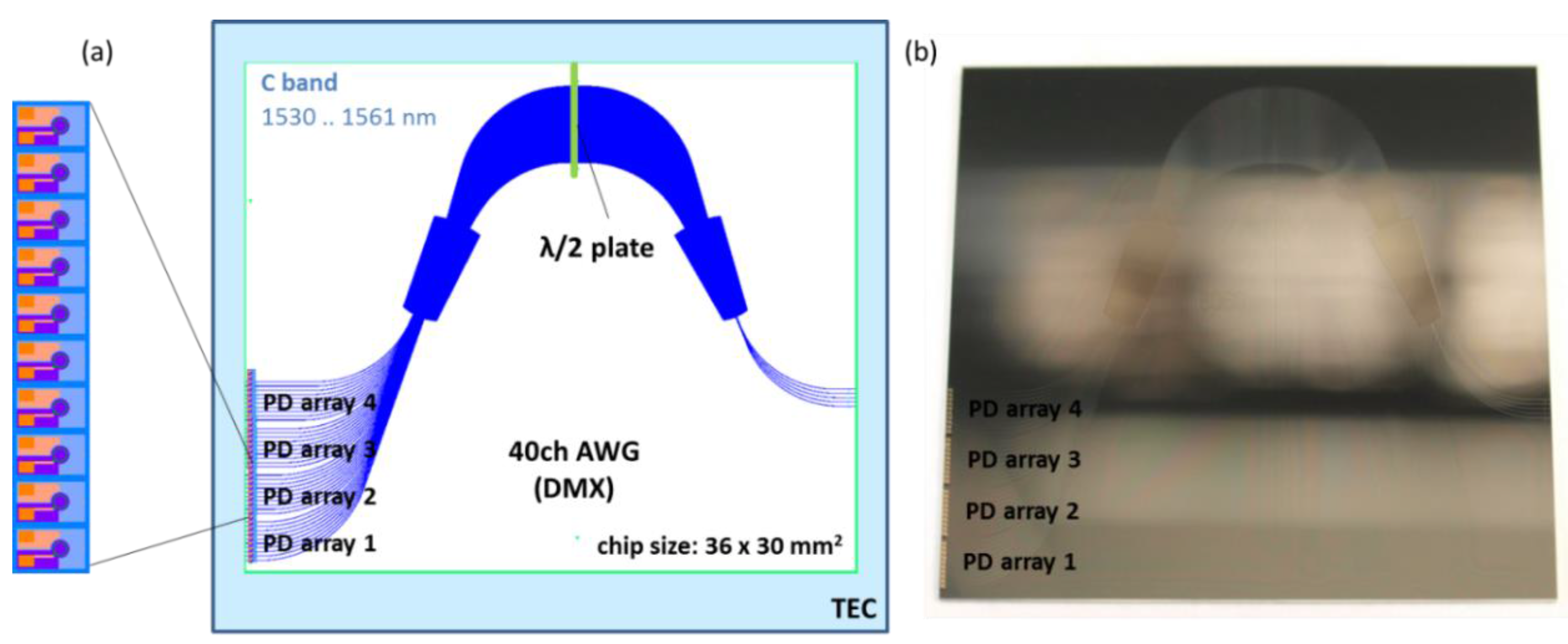
The OLT-Rx at the receiver side is shown in
Figure 8a,b. 4 × PD arrays, each containing 10 planar PDs are vertically coupled to the polymer DMX AWG by an integrated 45° mirror. The 40-channel polymer DMX AWG is designed to operate at 100-GHz channel spacing over the C-band (1534.2 nm–1561.4 nm). A λ/2 plate can be inserted via a deep etched slot in the middle of the arrayed waveguide region to minimize the polarization dependence [
2].
Figure 8.
40-channel OLT-Rx based on 4 × 10 planar PD arrays vertically coupled to a polymer AWG via an integrated 45° mirror. (a) The schematic layout and (b) photograph of the assembly.
Figure 8.
40-channel OLT-Rx based on 4 × 10 planar PD arrays vertically coupled to a polymer AWG via an integrated 45° mirror. (a) The schematic layout and (b) photograph of the assembly.
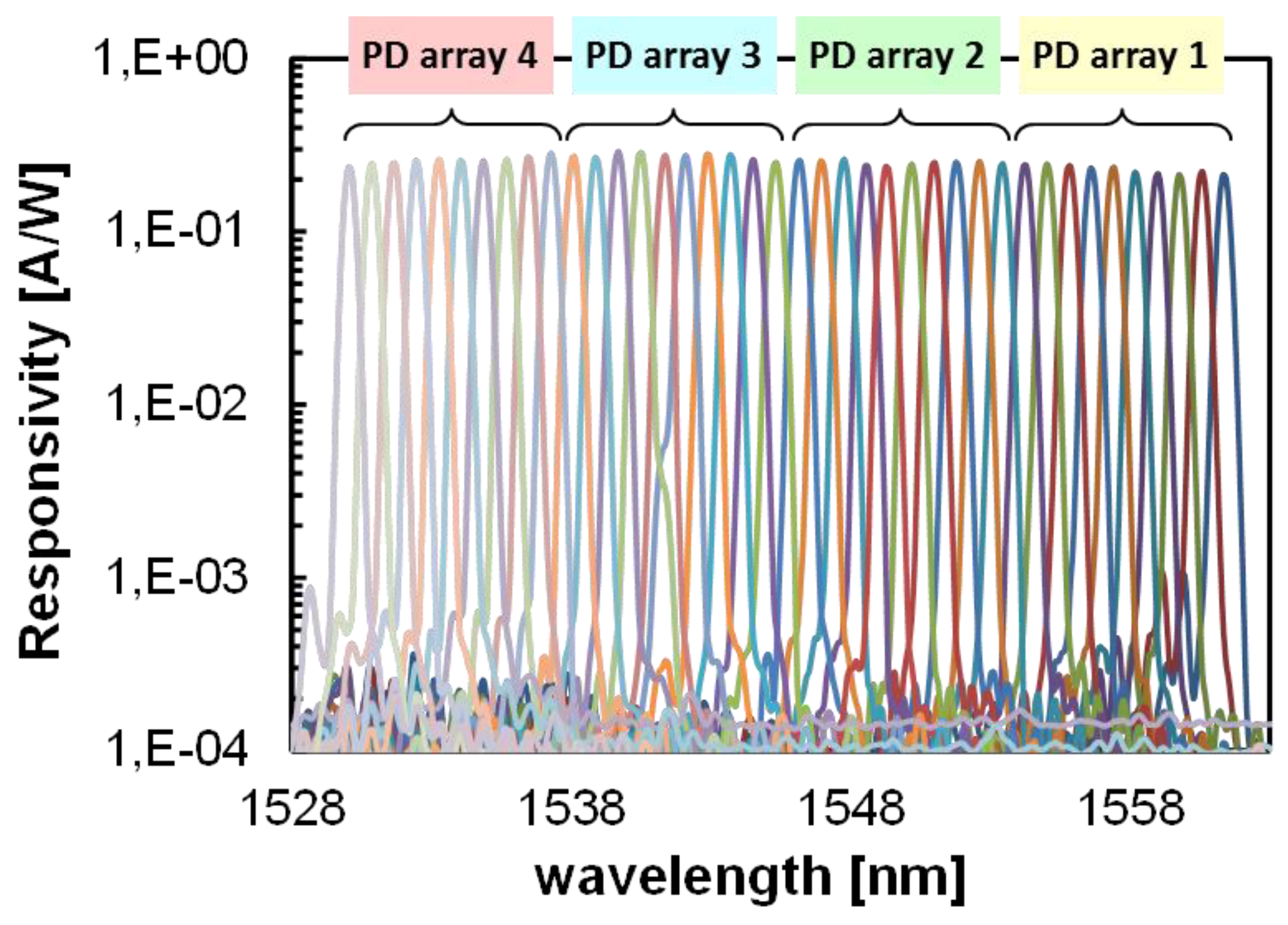
Figure 9 shows the responsivities of the OLT-Rx. For the measurements, the chosen PDs have an intrinsic responsivity of 1.1 A/W and an effective responsivity of ~0.22 A/W is obtained on the OLT. The device insertion loss, including the fiber coupling loss, mirror coupling loss and the propagation loss of the polymer AWG, is calculated to be ~7.5 dB. At somewhat compromised responsivity, the planar PDs have been reported to provide a bandwidth exceeding 30 GHz. With such PDs, each channel can reach a detection rate >25 Gb/s, and a total data rate over 1 Tb/s can be realized for such an OLT-Rx.
Figure 9.
Measured responsivities of the PD arrays on the OLT-Rx.
Figure 9.
Measured responsivities of the PD arrays on the OLT-Rx.
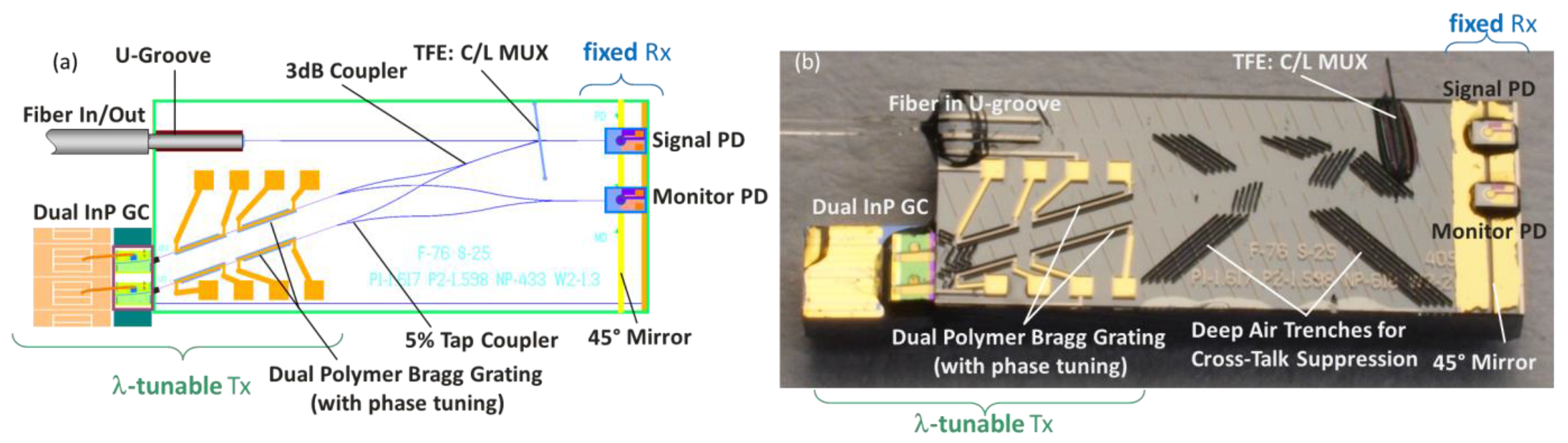
4. Colorless ONU
Within the WDM-PON technology, a colorless optical network unit (ONU) supporting all wavelength channels is needed to simplify network operation, reduce installation cost, and keep the maintenance efforts under control [
22,
23]. Such a device can be assembled on the polymer platform and functions including bi-directional connectivity, real-time data rate monitoring and crosstalk suppression can be enabled simultaneously [
14]. The schematic layout and the photo of the assembled ONU are shown in
Figure 10a,b. The entire assembly measures 6.5 mm (L) by 2.5 mm (W).
Figure 10.
ONU assembled on the polymer-based hybrid integration platform. (a) The schematic layout and (b) photograph of the assembly.
Figure 10.
ONU assembled on the polymer-based hybrid integration platform. (a) The schematic layout and (b) photograph of the assembly.
The InP gain chip (GC) is similar to an LD except that the internal optical feedback loop is intentionally removed. At least one facet of the gain chip is AR coated to eliminate internal lasing and enhance light emission. It usually employs a multi-quantum well design to enhance the output power and to broaden the gain bandwidth. The dual GC array is first placed and wire-bonded onto a RF-submount and then butt-joint coupled to the dual-channel polymer Bragg gratings. Together they form a tunable transmitter (Tx) when the GC is direct modulated. This dual-channel design helps relieve the thermal strain from the single polymer Bragg grating and the wavelength tuning across the C-band is split between the two paths. In this way, the local temperature at maximal tuning position still stays far below the certified degradation temperature of 300 °C and long-term stable performance is verified over more than 6000 h at stressed conditions [
24]. Five percent of the Tx power is tapped out via a pair of asymmetric Y-couplers to be received by the monitor PD. The TFE-based C/L band filter reflects the Tx signal, which further propagates through the polymer waveguide into the single mode fiber that is attached passively in the U-groove [
25].
On the receiver (Rx) side, the incoming optical signal at any wavelength within the L-band goes through the same fiber into the polymer waveguide. The TFE passes the signal through to the receiver side of the ONU, where the 45° mirror deflects the light and feeds it to the high-speed planar PDs mounted on top.
A series of air trenches are etched on the polymer chip together with the U-Groove and the TFE slot. These air trenches provide many optical interfaces and deliberately scatter the stray light in the polymer slab in the direction away from the location where the Rx PD is mounted to avoid cross-talks.
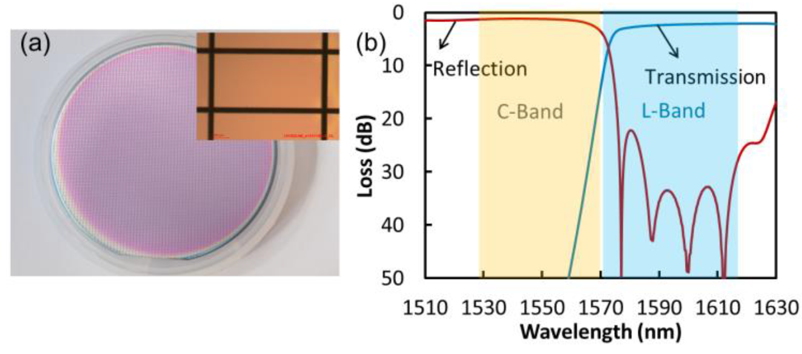
The TFE is a key element performing the C/L-band wavelength (de)multiplexing. It consists of alternating layers of sputtered SiO
2 and TiO
2 films on a thin polymer substrate. The total thickness of the filter adds up to 24 µm. The fabrication is done on a standard 3-inch silicon wafer. After sputtering, the TFE is cut by an excimer laser into desired dimensions. A photo of the TFE after cutting is shown in
Figure 11a. The TFE has been characterized by single mode fibers, prior to the integration into the polyboard. The reflection/transmission spectra are displayed in
Figure 11b. The TFE introduces a minimal insertion loss <2 dB. Due to the band-edge effect, however, the transition slope between 1562 nm to 1572 nm causes signals at these wavelengths to suffer from extra attenuation. Filters with steeper band-edges at reasonable thickness are currently being investigated.
Figure 11.
(a) Microscope image of the C/L band filter after laser cutting. (b) Reflection and transmission spectra of the TFE-based filter.
Figure 11.
(a) Microscope image of the C/L band filter after laser cutting. (b) Reflection and transmission spectra of the TFE-based filter.
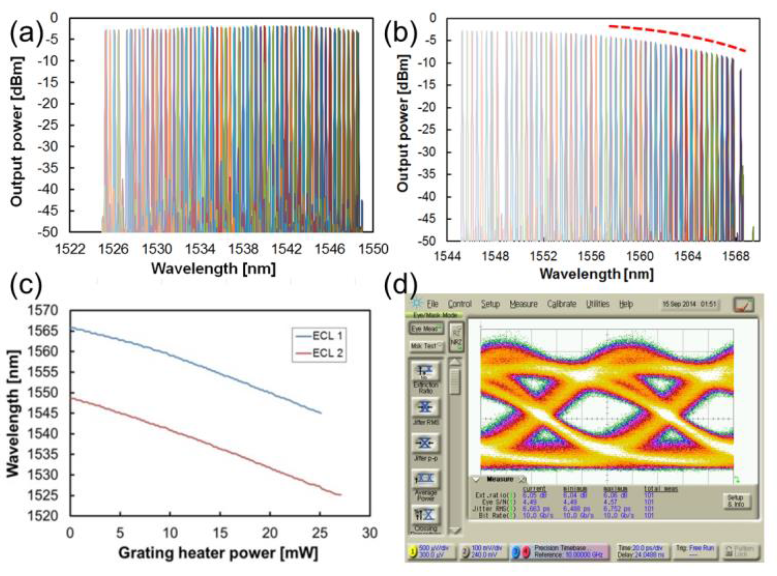
Figure 12.
(a) Tx characteristics of the ONU. Tuning spectra of the lower arm laser; (b) tuning spectra of the upper arm laser; (c) total tuning range and efficiency of both lasers; (d) eye diagram at 10 Gb/s after transmission through an 11.3-km-long standard single mode fiber.
Figure 12.
(a) Tx characteristics of the ONU. Tuning spectra of the lower arm laser; (b) tuning spectra of the upper arm laser; (c) total tuning range and efficiency of both lasers; (d) eye diagram at 10 Gb/s after transmission through an 11.3-km-long standard single mode fiber.
After the assembly, the ONU is first characterized on the Tx side. The drive current for the GC is set to 50 mA. The lower arm of the tunable laser path covers a tuning range from 1525 nm to 1548 nm, as indicated in
Figure 12a, while the upper arm from 1545 nm to 1568 nm, as shown in
Figure 12b. The side-mode suppression ratio is larger than 40 dB and the combined tuning range of 43 nm exceeds the C-band. The dropping of the laser output power at wavelength above 1560 nm is evidently affected by the band-edge of the TFE, as indicated by the dashed curve in
Figure 12b. The transmitter loss away from the band-edge region is around 7 dB from the GC to the fiber, including the 3-dB intrinsic loss of the Y-branch.
Both lasers show almost identical thermal tuning behavior and the efficiencies are plotted in
Figure 12c. For each laser to reach 23 nm wavelength tuning, only ~26 mW heater power is needed. The thick polymer bottom cladding and the deep-etched air trenches surrounding the buried heaters function as ideal thermal buffers [
24,
26,
27]. The tuning efficiency reaches 0.88 nm/mW.
The Tx laser can be direct modulated on the GC at 10 Gb/s data rate [
24,
28,
29]. The eye diagram after transmission along an 11.3-km-long standard single mode fiber (SSMF) is shown in
Figure 12d. The signal to noise ratio is 5.85 dB and the bit error rate (BER) is lower than 1 × 10
−13. No band-pass filter is used in the experiment.
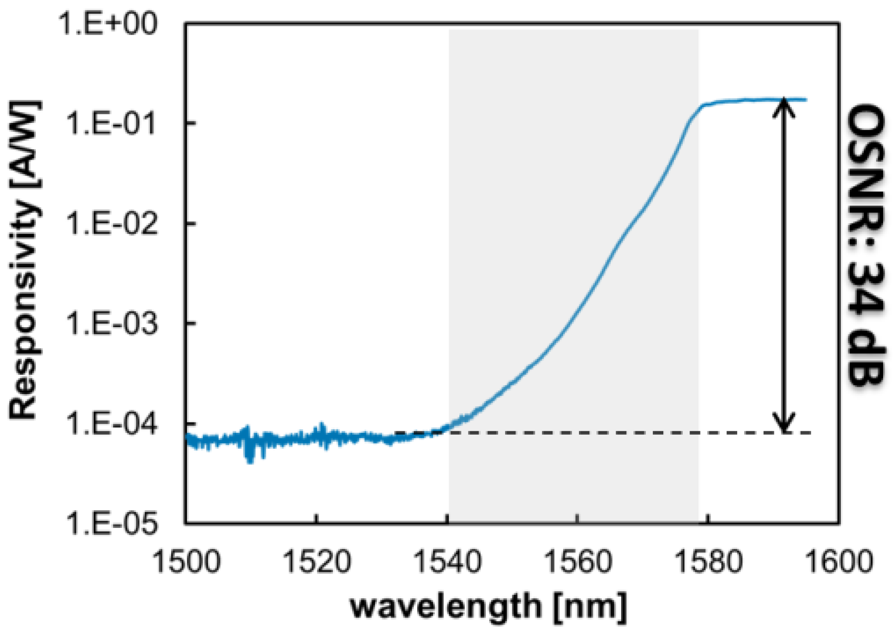
On the Rx side, a broadband tunable laser source is injected into the fiber and the signal PD responsivity is shown in
Figure 13. Above 1580 nm, the PD responsivity remains at 0.14 A/W, corresponding to a receiver loss of ~7 dB from the fiber to the PD. The mirror loss amounts to ~1 dB. The fiber/waveguide coupling and the waveguide propagation loss add up to ~2 dB. The rest is attributed to the TFE loss, ~2 dB concluded from the measurement using fibers, and the associated scattering loss at the TFE/waveguide interface in the slot. The scattering loss is caused by the non-optimal wave-front matching from the free-space region (TFE and excess slot width) to the receiving waveguide,
i.e., the mismatch between the broadened beam (location and size) and the near-field mode profile of the waveguide. This loss can be reduced by introducing proper tapers and waveguide offsets at the slot region. The optical signal to noise ratio (OSNR) is measured to be 34 dB at 1580 nm and 1540 nm.
Figure 13.
Responsivity measurement of the signal PD at different wavelengths.
Figure 13.
Responsivity measurement of the signal PD at different wavelengths.
5. Dual-Polarization Coherent Receiver
The exponential growth of the internet traffic is pushing the optical fiber technology from the current 112 Gb/s links based on the DP-QPSK coherent transmission scheme to 400 Gb/s and further beyond 1 Tb/s using dual-polarization 16-QAM up to 128-QAM [
30]. On the receiver side, an optical 90° hybrid is required as the frontend to convert the phase modulated signal into amplitude variations detectable by the balanced PDs [
31,
32]. The in-phase and quadrature components of the optical signals are then extracted as photo current variations. Further on, with the help of trans-impedance amplifiers (TIAs) and analog-to-digital converters (ADCs), the electronic signals are amplified and digitalized. Complex digital signal processing (DSP) algorithms are applied to compensate, synchronize, recover and separate the densely encoded signals.
The phase-mixing function of the optical 90° hybrid requires a laser source as local oscillator (LO). A colorless optical 90° hybrid must be able to handle a broad wavelength range, e.g., the C-band, and accordingly the LO should be tunable over that range. To bring down the device footprint, power consumption, packaging efforts and costs, an integrated, low-cost and wavelength tunable LO is highly desired.
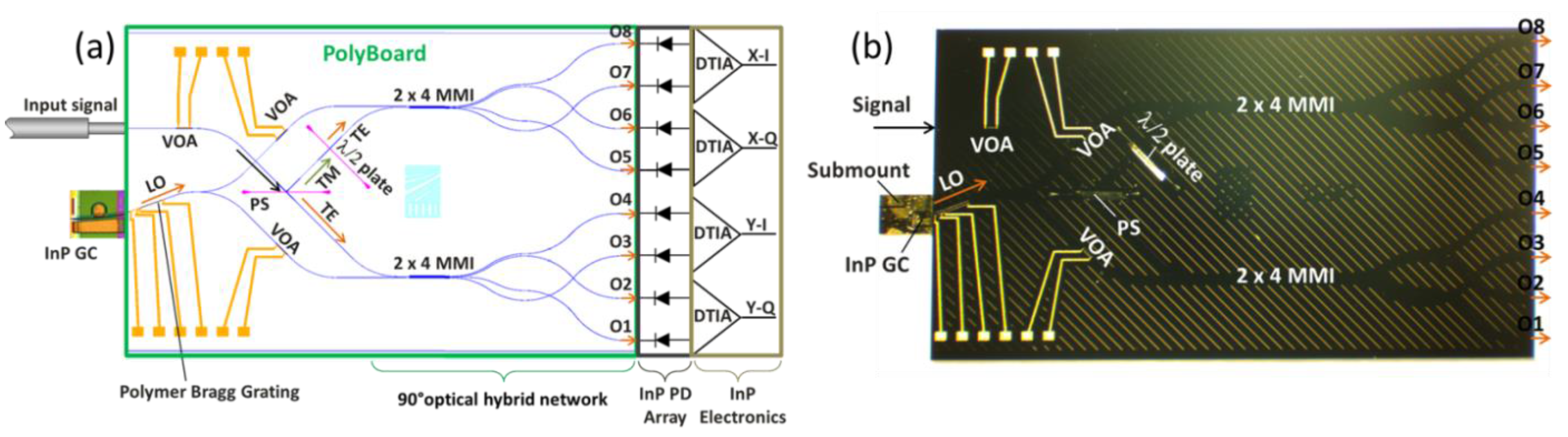
The schematic layout of the hybrid coherent receiver is displayed in
Figure 14a. The device relies heavily on the hybrid integration technology: the polyboard provides low-loss waveguide components including bends, tapers and multi-mode interference devices (MMIs), as well as thermo-optic components including tunable Bragg gratings and variable optical attenuators (VOAs) [
33,
34]; the thin-film elements, based on the mixed layers of polymers and dielectrics, are used to split and rotate the polarization states; InP photonics platform provides the light source (GC) and the high-speed (100G) waveguide PD array: InP electronics platform offers high-speed differential trans-impedance amplifier (DTIA) and DMX circuits. The optical and electronic layouts from these components need to be arranged collectively to ensure a conflict-free assembly process. For this reason, the polymer output waveguides are extended to reach the same pitch (1 mm) as the waveguide-based PD array. The space is also reserved for a matched wire-bonding process to connect the 4 × InP-based DTIA array for the electronic signal processing.
Figure 14.
(a) Schematic layout of a coherent receiver consisting of a polymer-based 90° hybrid with integrated LO, 8 × InP PD array, and 4 × InP DTIA array. (b) Photograph of the assembled polymer-based 90° hybrid.
Figure 14.
(a) Schematic layout of a coherent receiver consisting of a polymer-based 90° hybrid with integrated LO, 8 × InP PD array, and 4 × InP DTIA array. (b) Photograph of the assembled polymer-based 90° hybrid.
On the polyboard, the Bragg grating is coupled to the InP GC to form the tunable LO. Three VOAs are added, both in the signal path and the LO path, to provide extra flexibility in handling signals with potentially large time- and polarization-dependent amplitude variations. The contact pads for the thermal electrodes are arranged on the top- and bottom-left side of the chip so that the electrical connections (DC) can be made in an orderly manner to the pins on the housing. Two 2 × 4 MMIs are used for the phase mixing and decoding. The thin-film-based polarization splitter (PS) separates the TE (transmitting) and TM (reflecting) components, and the half-wave (λ/2) plate rotates the TM light back to TE polarization. In this way, the MMIs and the PDs only need to be optimized for the TE polarization. It is worth noting that the PS usually causes higher loss for the transmitted TE path (~1.3 dB) than the reflected TM path (~0.5 dB). With waveguide tapers, the λ/2 plate introduces a loss of ~1 dB on the TM path, which balances out the loss imbalance and helps to generate more uniformly distributed output powers among the two mixer MMIs.
The assembled colorless dual-polarization 90° hybrid as the coherent receiver frontend has been demonstrated [
35]. A photo of the assembly is shown in
Figure 14b. The characterization results are summarized in
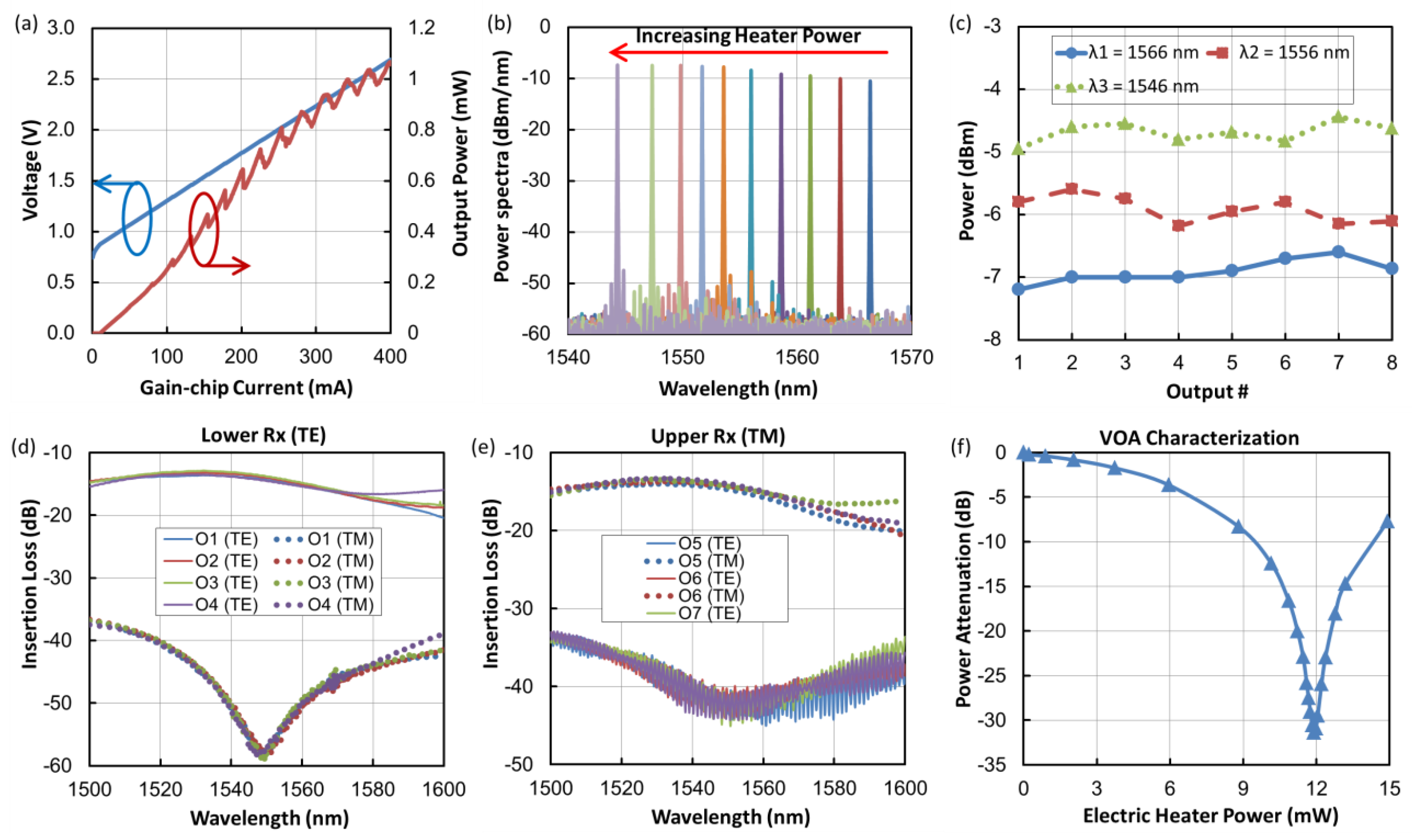
Figure 15. The P-I and V-I characteristics of the LO are shown in
Figure 15a, measured in the fiber at O1. The initial wavelength is 1566 nm. The output power reaches beyond 1 mW at ~400 mA gain current. Higher output power can be achieved by using InP GCs with prolonged gain region. The ripples in the P-I curve is caused by the mode-hopping and can be compensated by adjusting the phase-electrode included in the laser cavity. The LO can be continuously tuned over 22 nm, as demonstrated in
Figure 15b. The side mode suppression ratio is larger than 40 dB. The power imbalances among the eight outputs are evaluated at three selected wavelengths, as summarized in
Figure 15c. The power fluctuations among the wavelengths agree well with the 2 × 4 MMI measurements from the signal path and can be minimized by adjusting the MMI structures.
Figure 15.
Characterization results of the assembled 90° hybrid: (a) P-I and V-I curve of the LO; (b) overlaid spectra of the LO during tuning; (c) LO power comparison at the 8 outputs at three different wavelengths; (d) the lower Rx O1–O4 for the TE component of the signal path; (e) the upper Rx O5–O8 for the TM component of the signal path; (f) the on-chip VOA.
On the signal path, the eight outputs are evaluated by injecting a broadband light source with controlled polarization states. The results are displayed in
Figure 15d,e. Both the upper and lower Rx appear to have similar performances, with an average insertion loss of ~13.3 dB at 1530 nm and 15.5 dB at 1565 nm, including 6 dB MMI intrinsic loss, 1.5 dB fiber coupling loss (both facets), 3 dB waveguide loss (propagation + bending), 1.5 dB polarization controller loss (PS + λ/2 plate), 0.5 dB VOA loss, and 0.8–3 dB MMI excess loss across the C-band (1535 nm–1575 nm). The power imbalance among all eight outputs is below 1 dB and the polarization extinction ratio is larger than 25 dB across the C-band. The characterization results of the on-chip VOAs are shown in
Figure 15f. At 12 mW electric heater power, the VOA reaches an attenuation level of 32 dB.
In the first attempt to integrate both tunable LO and VOAs on an optical 90° hybrid with dual-polarization functionality, the thermo-optic components, MMIs, and polarization controllers are all functioning properly without any noticeable optical and thermal cross-talk. To improve the performance, the tuning range of the LO can be expanded, e.g. by using a dual-grating structure and a Y-branch-based thermo-optic switch [
29,
33,
36], to cover the full C-band. The MMI structure can be adjusted to shift the minimal loss band toward the center of the LO tuning range.
To summarize the hybrid integration technology presented in
Section 3,
Section 4 and
Section 5, the fibers and the TFEs can be inserted passively and secured by UV-epoxy in their defined grooves and slots. The attachment of the planar PDs is assisted by a fine-placer with a positioning accuracy of ±1 µm. The process can be carried out passively with the help of the alignment marks on the chip. In the case of critical coupling of high-speed PDs with small active areas, the process can be switched to active alignment with a specially designed holder that provides electrical connections. In both cases, the exact PD location is calculated from the actual mirror width and the vertical location of the buried waveguide. Fully automated and scalable processes are being tested for the passive fiber and PD attachment.
The gain chip, LD and LD array alignment is active at the moment. The optimal position is fixed once the maximal optical power is obtained at the monitored output. An automated assisting tool has been implemented for fine-alignment using six-axis stages and nano-force sensors.
The assembly process is reproducible and the hybrid technology is well proven in the demonstrated devices. In our lab, we have assembled tens of the tunable lasers and around 80% pass our internal tests with minimal performance variation.
6. Wavelenght Tunable 100G Transmitter Module
The polyboard technology has also contributed to the establishment of an advanced hybrid integration platform incorporating: (1) EO polymers for constructing low-complexity and low-cost Mach-Zehnder modulators (MZMs) with extremely high modulation bandwidth (>100 GHz); (2) InP components for light sources, detectors, but also high-speed electronics including MUX drivers and DEMUX circuits; (3) Ceramic (AlN) RF board and interposer that interconnects and terminates the electronic signals within the package. The entry of polyboard has not only enabled the functionalities such as wavelength tuning, polarization management, and light-flow (amplitude and direction) control, but also brought along well developed passive components (AWGs, MMIs and so on) and improved the integration compatibility with InP-based active devices and passive thin-film elements.
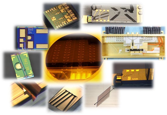
Figure 16.
Dissecting of the tunable 100G optical transmitter utilizing the merits of the four material systems. From lower-right counterclockwise: EO polymers for high-speed light modulation; InP-DHBTs for ultrafast driver electronics; ceramic RF board for electronic signal interconnects and termination; polyboard for wavelength tuning and polarization control.
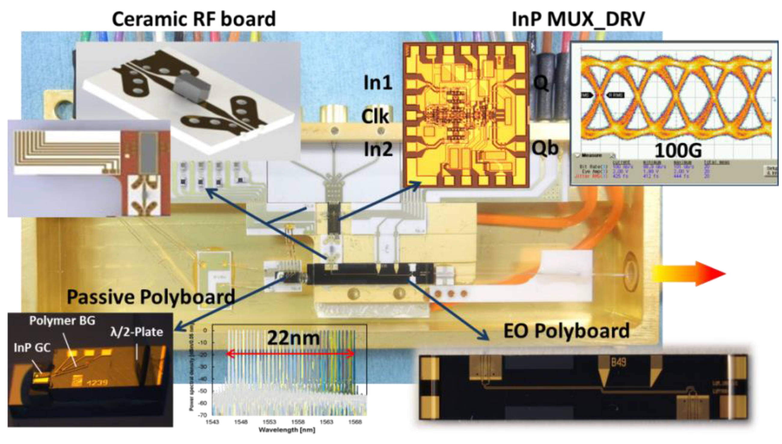
On this hybrid integration platform, a wavelength tunable, 100 Gbaud, all-in-one transmitter module has been demonstrated [
19]. The dissecting of the module is displayed in
Figure 16. The passive polyboard includes a thermally-tunable Bragg grating section and an optically coupled interface with the InP-based gain element. An external-cavity tunable laser is hereupon assembled; the half-wave plate inserted at the output waveguide efficiently converts the TE emitting laser to the required TM polarization that feeds into the EO polymer MZM.
Electro-optical (EO) polymers have been known to possess extremely fast EO responses. A modulation bandwidth larger than 100 GHz has been achieved [
37,
38], paving way for the advanced, complex and high-fidelity signal generations in optical communications. The polymer modulator fabrication process replies on the low-temperature thin-film-polymer on silicon (TFPS) technology [
38]. The fabrication can scale up with silicon wafer size and is compatible with industry-standard semiconductor manufacturing techniques. Within this technology a poling process is required with the electric field oriented perpendicular to the wafer and the ultrafast electro-optic effect only exists for the TM polarized light. Since most LDs are developed for the TE polarization, the direct attachment of a laser source raises some challenges. The previous solution replies on the 90° rotated attachment [
14,
15,
16]. Novel as this method is, the assembly process is complex and time-consuming. With the introduction of the polyboard, the polarization can be converted prior to the attachment. The assembly can be simplified and secured.
The electronic signal multiplexers and drivers (MUX-DRV) are fabricated on an InP-double heterojunction bipolar transistor (InP-DHBT) process. The architecture choice for this application, operating at very high bit-rate, has been to monolithically integrate a multiplexing stage with 3R function (re-amplifying, re-shaping, and re-timing). In this architecture, the electrical input interface operates at lower, half-rate speed and the 100 Gb/s electrical interfaces on chip are shortened to the minimum. The clean multiplexed signal is directly applied to amplifying stage. Two versions of InP DHBT 2:1-selector-driver have been fabricated using the 0.7 μm InP-DHBT technology [
39]: with the compact lumped amplifier [
40] and with distributed amplifier [
41]. The differential output eye diagram of the distributed amplifier operating at 112 Gb/s has reached an amplitude of 5.9-Vpp, leading to a new record swing-speed product of 660 VGb/s.
At high speed, the electronic interconnect becomes challenging. Improper RF arrangement can throttle the overall system bandwidth to a level much below the capacity of the individual components. The RF links cannot solely rely on the bond-wires, as the dangling wires with varying structural and contact properties often lead to severe signal deterioration, interference and unbalanced transmission. An interposer is often needed to connect the electronic signals among the components and also to the cable connectors on the housing. The interposer can be fabricated by structuring metal transmission lines on a ceramic film. The design must be compatible with the housing as well as the overall placement of the individual components to avoid interference, back-reflection and other possible signal impairment. The package shown in
Figure 16 is based on the gold-plated submounts of CuW that provide mechanical support for the optical and electrical components. Also included in the package are DC and RF coupling substrates, active thermal control with a thermo-electric cooler (TEC), and a lensed fiber for the coupling of the modulated signals out of the box.
The optical loss of the transmitter module is estimated to be ~12.5 dB. This includes the propagation loss on the passive polymer and the EO polymer chip, the insertion loss of the half-wave plate and the MZM, the coupling loss between the passive and the EO polymer chip and the coupling loss between the EO polymer chip and the lensed fiber. The power consumption of the device is around 7.2 W, taking into account the consumption of the tunable laser (0.25 W for the GC and max. 0.06 W for the thermal tuning), the MUX-DRV circuit (3.8 W), the phase-shifter for the biasing of the MZM (0.04 W), and the TEC (around 3 W).
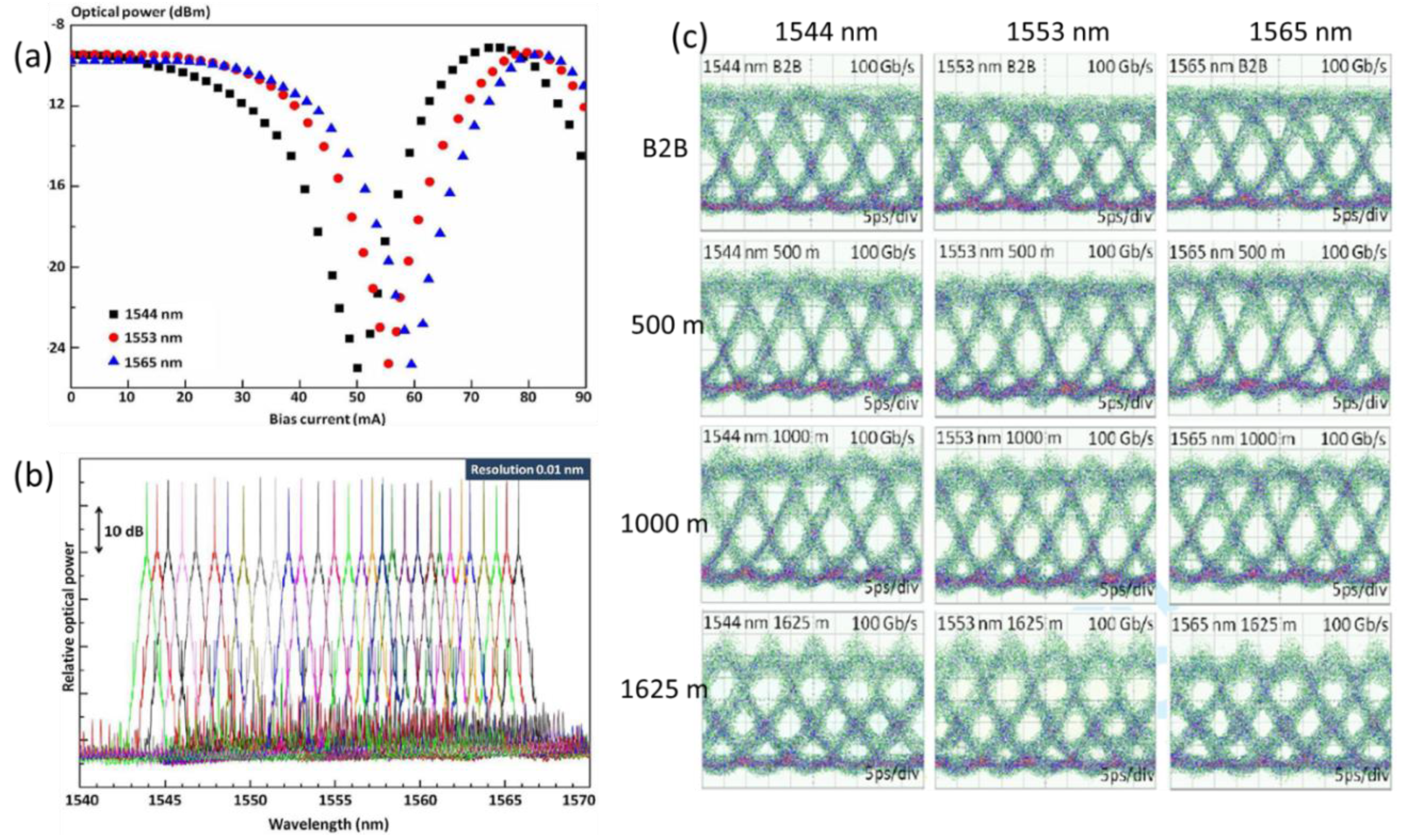
Figure 17.
(a) The DC characteristics of the transmitter module at 1544 nm, 1533 nm and 1565 nm. (b) overlaid spectra of the 100 Gb/s on-off keying (OOK) signals at the output of the transmitter module covering the tuning range from 1544 nm to 1566 nm. (c) Eye-diagrams of the 100 Gb/s OOK signals, evaluated at three wavelengths from B2B to 1625 nm SSMF transmission.
The DC characteristics of the transmitter module, plotted in
Figure 17a, are obtained by adjusting the bias current of the thermal phase shifter on one of the MZM arms. Three wavelengths are selected within the tuning range from 1544 nm to 1566 nm. The static extinction ratio is around 16 dB and the maximal output power reaches −9.5 dBm. The overlaid wavelength tuning spectra are summarized in
Figure 17b, which are collected directly at the output of the transmitter when modulated with on-off keying (OOK) signals at 100 Gb/s. Continuous wavelength tuning from 1544 nm to 1566 nm has been demonstrated. The typical tones of the OOK modulation can be seen on both sides of the carriers with 100 GHz (0.8 nm) spacing.
The transmission performances at 100 Gb/s data rate are evaluated at the three selected wavelengths and the eye-diagrams are recorded for the back-to-back (B2B) transmission and propagation through a SSMF up to 1625 m. The results are listed in
Figure 17c. The characteristics at the three wavelengths are very similar and the eyes remain open after 1625-m SSMF transmission. However, when the transmission distance goes beyond 1000 m, the chromatic dispersion in the SSMF starts to degrade the signal quality, indicated by the immerging hills on the top of the eye diagram. Further experiments show that error free transmission with BER lower than 10
−10 is achievable at 100 Gb/s for a distance up to 500 m, beyond which the BER increases to 10
−9 for the 1000-m and 10
−7 for the 1625-m transmission, respectively. Forward error correction (FEC) coding or dispersion management in the fibers will then be needed.
The all-in-one packaged transmitter module allows direct plug-n-play deployment in the optical network systems. The single-lane 100 Gb/s connectivity can significantly reduce the number of components, shrink down device footprint and improve the network flexibility. Compared to higher-order modulation formats, the serial OOK approach is also an economical solution in terms of system complexity, number of components needed for signal generation and detection, latency, footprint, overall power consumption, and so on. The wavelength tunability can further resolve contentions, improve efficiency, and bring flexibility to the network.
To exploit this integration platform further, the MZMs and the drivers can form arrays and scale up to 400 Gb/s transmission. Combined with coherent transmission schemes and higher-order modulation formats, the transmitter can provide 1 Tb/s data rate and beyond, in which case a 3D opto-electronic integration is to be implemented, in order to distribute the electronic signals smoothly and evenly among the modulator array [
3]. Besides the demonstrated wavelength tunability and polarization management, the polyboard can bring a switching matrix based on thermo-optic switches and enable the multi-flow control of the optical circuits, a function that empowers the software defined network (SDN) directly down to the optical circuit level but is deemed too expensive to be implemented on any other integration platforms. This hybrid integration platform is bound to bring new insights on the general photonic integration paradigm and serves to impact the strategic plans for the deployment of the advanced photonic devices in the telecom and datacom industry.
7. Conclusions
The polymer-based hybrid integration technology is reviewed in this work. The polymer materials can be synthesized and tested prior to the fabrication. The low-temperature layer formation process is simple and fast, leading to a substantial fabrication cost reduction. Deep grooves, trenches and slots are etched with oxygen-based RIE with a metal-mask selectivity exceeding 500. Fibers, TFEs and PDs can be passively inserted in/attached on the chip, reducing also the assembly cost.
Furthermore, multi-layer polymer waveguides and multi-step 45° mirrors enable the 3D construction of the photonic integrated circuits. Silicon nitride has been introduced as core material, and heterogeneous waveguide components are realized, opening up possibilities to incorporate inorganic materials in polymer and combine their properties for multi-functional devices.
For practical devices, 40-channel OLTs have been assembled, also proving the feasibility of integrating large arrays of LDs and PDs on the polyboard. Equipped with a thin-film filter, an on-chip fiber groove and a 45° mirror, a compact ONU device is realized, allowing bi-directional transmission in the C band and detection in the L band. For applications in coherent detection, a 90° hybrid is demonstrated with integrated LO and VOAs.
The polyboard has been further incorporated into a larger hybrid integration platform together with EO polymer modulators, InP electronics and ceramic RF interconnects. This powerful platform has yielded an all-in-one, 22-nm wavelength tunable, 100 Gbaud transmitter module that not only delivers state-of-the-art performance but also allows direct plug-and-play deployment in the optical network systems. With more advanced, multi-flow transmitter modules under way, this polymer-based hybrid integration platform is only starting to unleash its full potential and is bound to bring photonic integration to a new, unprecedented level.
Comparing to other integration platform like SOI or InP, the advantage of polymer platform lies in the low-cost fabrication technology, the possibility to realize multi-layer optical circuits, the flexibility and capability to integrate a large variety of optical functions. For applications, where several functions must be integrated on space smaller than a couple of mm2, other integration technologies may be more appropriate.

 ,
, 