Monolithically Integrated Ge-on-Si Active Photonics

Thayer School of Engineering, Dartmouth College, 14 Engineering Drive, Hanover, NH 03755, USA
Photonics 2014, 1(3), 162-197; https://doi.org/10.3390/photonics1030162
Submission received: 27 May 2014
/
Revised: 19 June 2014
/
Accepted: 19 June 2014
/
Published: 2 July 2014
Abstract
:Monolithically integrated, active photonic devices on Si are key components in Si-based large-scale electronic-photonic integration for future generations of high-performance, low-power computation and communication systems. Ge has become an interesting candidate for active photonic devices in Si photonics due to its pseudo-direct gap behavior and compatibility with Si complementary metal oxide semiconductor (CMOS) processing. In this paper, we present a review of the recent progress in Ge-on-Si active photonics materials and devices for photon detection, modulation, and generation. We first discuss the band engineering of Ge using tensile strain, n-type doping, Sn alloying, and separate confinement of Γ vs. L electrons in quantum well (QW) structures to transform the material towards a direct band gap semiconductor for enhancing optoelectronic properties. We then give a brief overview of epitaxial Ge-on-Si materials growth, followed by a summary of recent investigations towards low-temperature, direct growth of high crystallinity Ge and GeSn alloys on dielectric layers for 3D photonic integration. Finally, we review the most recent studies on waveguide-integrated Ge-on-Si photodetectors (PDs), electroabsorption modulators (EAMs), and laser diodes (LDs), and suggest possible future research directions for large-scale monolithic electronic-photonic integrated circuits on a Si platform.
1. Introduction
In our information age, information and communication technology (ICT) already consumes ~5% of electricity worldwide in 2012 [1]. Considering that the data traffic has grown 30× from 2010–2015 [2], this number will increase to >10% by 2020 in developed countries [3] and become a significant part of energy consumption in the 21st century. More than half of the energy is consumed by interconnects that transfer information from one place to another, rather than computation itself. Electronic-photonic integrated circuits (EPICs) on Si have become an increasingly appealing solution to this issue [4,5]. They combine the merits of photons in energy-efficient, high bandwidth data transmission with the merits of electrons in high-speed data processing on a single microchip, providing the most efficient synergy for Green ICT [6].
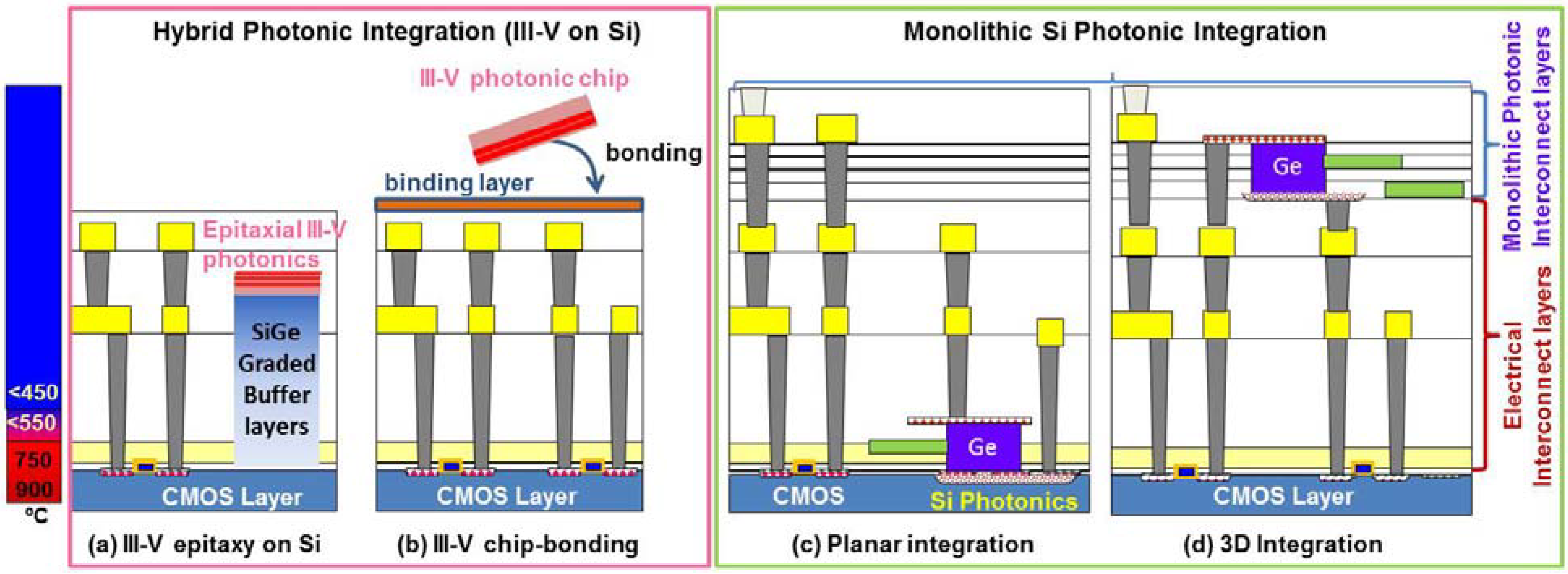
A significant challenge for high-volume, large-scale EPICs on Si is active photonic devices for light generation, modulation and detection. These devices are conventionally based on direct band gap III-V semiconductors to benefit from the efficient direct gap transitions. However, epitaxial growth of high-quality III-V semiconductors on Si typically requires a thick buffer layer due to the lattice mismatch, making it difficult to integrate with complementary metal oxide semiconductor (CMOS) circuits (Figure 1a). Hybrid integration of III-V devices on Si by chip bonding has achieved significant progress in recent years, yet scaling to high-volume, wafer-scale processing is limited by the difficulties in incorporating III-V device fabrication into a standard CMOS processing flow.
Figure 1.
Schematics of hybrid photonic integration vs. monolithic Si photonic integration. Hybrid integration with III-V semiconductors includes (a) III-V epitaxy on Si, and (b) chip-bonding of III-V on Si. Monolithic Si photonic integration includes (c) Planar integration of Si photonics with complementary metal oxide semiconductor (CMOS) circuits on the same layer, and (d) 3D photonic integration with the photonic interconnect layer positioned well above the CMOS layer. In (c) and (d), waveguide-coupled Ge photo detectors are shown as examples of CMOS-compatible, monolithic photonic devices. The color bar on the left shows the processing temperature in different layers.
Active photonic devices based on Si itself have also been extensively studied in the past decade. While Si electro-optical modulators based on carrier-induced refractive index changes have achieved great success [7,8,9], the trade-off between operation wavelength range and energy consumption/thermal stability is still hard to overcome [9,10]. Conventional Mach-Zehnder interferometer (MZI) structures tend to have large footprints with high power consumption, while energy-efficient micro-resonator modulators have limited operation wavelength range and tend to suffer from resonant peak shifts due to thermo-optical effects. Si nanostructures have been investigated for light emission [11,12], and defects states have been engineered to extend the absorption range of Si for photodetection at telecommunication wavelengths [13,14]. However, the difficulty in electrical injection limits the efficiency of Si nanostructure light emitting diodes (LEDs). While high electroluminescence efficiency has been observed in Si nanocrystal-organic hybrid systems at very low injection levels; at elevated injected current density >1 mA/cm2 the efficiency drops dramatically [15]. The spectrally extended Si photodetectors (PDs) using engineered defect states suffer from a low absorption coefficient and a trade-off in quantum efficiency particularly at CMOS-compatible driving voltages (<5 V).
To address the limitations of III-V semiconductors and stand-alone Si, since the late 1990s Ge has become an interesting candidate for active photonic devices on Si platforms due to its pseudo-direct gap behavior [16] and compatibility with Si CMOS technology [17]. Utilizing the efficient direct gap transition of Ge and band engineering techniques to further reduce the energy difference between the direct and indirect band gaps, high-performance Ge-on-Si PDs, electroabsorption modulators (EAMs) and prototype laser diodes (LDs) have been demonstrated in recent years. While epitaxial Ge-on-Si materials and devices comprise the main approach so far (Figure 1c), recent research is also exploring the possibility of monolithic 3D integration using back-end-of-line (BEOL) CMOS processing (Figure 1d). In this paper, we review recent progress in band engineering, materials growth and the design/performance of integrated Ge active photonic devices on Si. We also propose some possible directions for future investigations. The results demonstrate that Ge-on-Si is an ideal solution for monolithic, large-scale electronic-photonic integration.
2. Band Structure and Band Engineering
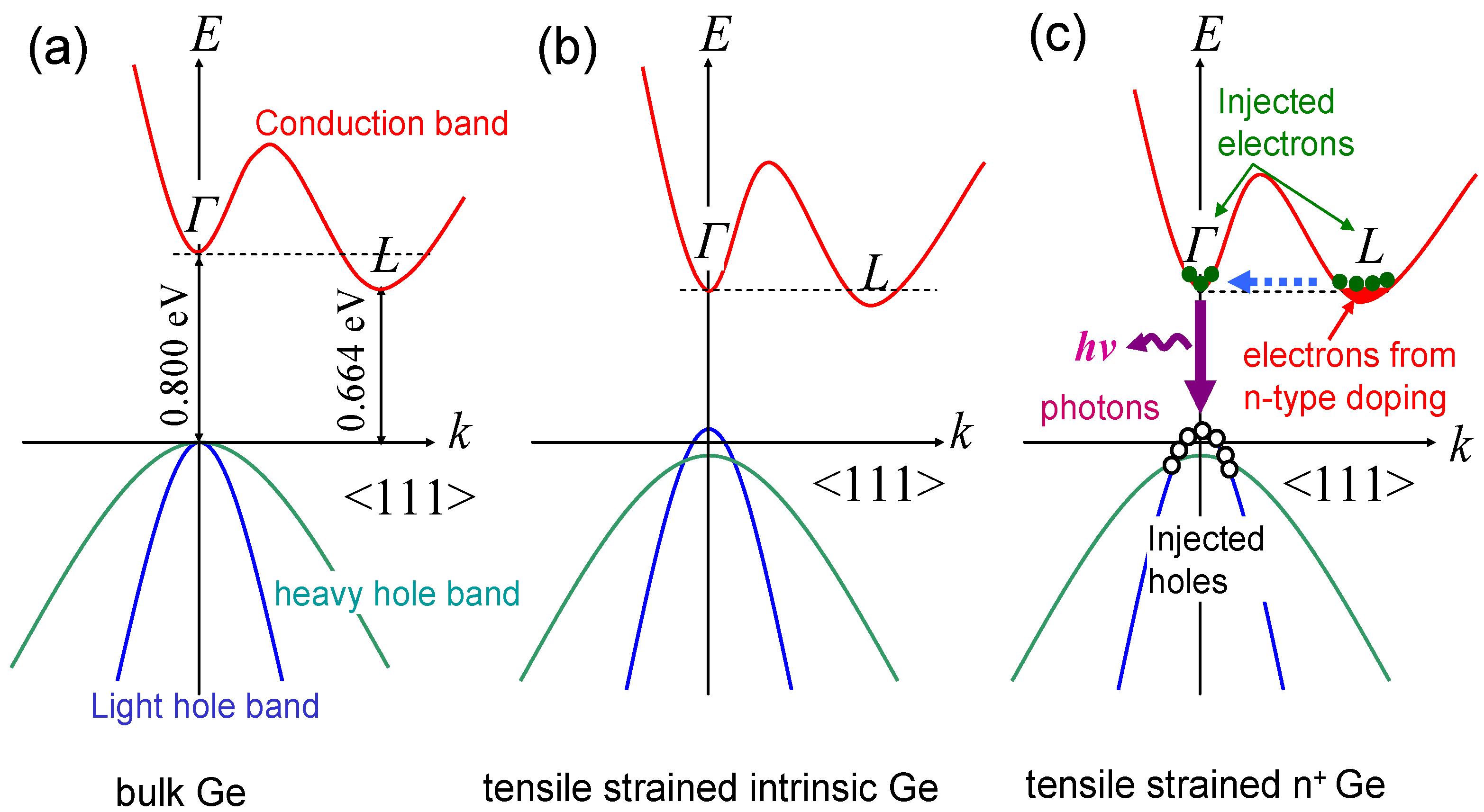
The band structure of bulk Ge is schematically shown in Figure 2a. Although Ge is considered an indirect gap semiconductor, the energy difference between its direct gap at the Γ valley and indirect gap at the L valleys is only 136 meV [16], or ~5 kBT at room temperature (kB is the Boltzmann constant). The direct band gap of 0.8 eV corresponds to a wavelength of 1550 nm, the most technically important wavelength in optical communications. Active Ge photonic devices on Si are fundamentally based on this direct gap transition. In this section, we will discuss several band-engineering approaches that transform Ge towards a direct gap semiconductor.
2.1. Tensile Strain
The energy difference between the direct and indirect gaps of Ge can be further reduced by tensile strain, as schematically shown in Figure 2b [18,19]. With biaxial tensile stress, both direct and indirect gaps shrink, but the direct gap shrinks faster. Therefore, Ge transforms from an indirect towards a direct gap semiconductor with the increase of tensile strain. Furthermore, the top of the valence band is determined by the light hole band under biaxial tensile stress. The small effective mass of the light hole band reduces the density of states in the valence band, which in turn decreases the threshold for optical transparency and lasing. Theoretically, Ge can be transformed into a direct gap material with ~2% biaxial tensile strain [19,20,21] or >4% uniaxial tensile strain along <100> direction [22]. The band gap decreases to ~0.5 eV correspondingly. Experimentally, a thermally induced tensile strain of 0.2%–0.3% can be obtained in the Ge thin films utilizing the difference in thermal expansion coefficients between Ge and Si [23,24,25]. This level of tensile strain reduces the difference between the direct and indirect band gaps of Ge from 136 to ~100 meV, and redshifts the direct band gap from 0.8–0.76 eV. Several approaches have been investigated to further enhance the tensile strain in epitaxial Ge. These include growths on relaxed GeSn buffer layers [26,27], utilizing silicide [28] and nitride stressor layers [29,30], and coupling micro-electromechanical systems (MEMS) with suspended thin Ge layers. Jain et al. [31] have demonstrated a prototype MEMS device with up to 1.4% uniaxial and 1% biaxial tensile strain introduced to the Ge layer by a Si3N4 stressor. Compared to bulk Ge, the photoluminescence (PL) peak redshifts to λ = 1860 nm (hν = 0.64 eV) and the integrated intensity increased by 260 times. More recently, Süess et al. [32] achieved 3.1% uniaxial tensile strain in a suspended Ge beam by patterning and under-etching 0.15% tensile strained Ge thin films grown on Si and silicon-on-insulator (SOI) substrates. This approach utilizes the fact that, at a constant force in the plane of the Ge films, the stress is inversely proportional to the cross-sectional area of the suspended structures. Since the suspended beam can be patterned into a very small cross section, the stress in this region is greatly enhanced compared to the blanket film regime. The direct band gap shrinks by 0.21 eV to hν = 0.59 eV (λ = 2100 nm) in this case, and the PL intensity increases by 25 times. Further increase in strain is only limited by the mechanical strength of Ge itself. Indeed, very lately the same group has further achieved 4% uniaxial strain [33], while Sukhdeo et al. have reported 5.7% tensile strain along <100> direction [34]. In addition, Capellini et al. have reported up to ~0.9% equivalent biaxial tensile strain in a SiN(stressor)/Ge/SOI(001) stack using 130 nm bipolar-CMOS (Bi-CMOS) processing [35].
Figure 2.
(a) Schematic band structure of bulk Ge, showing a 136 meV difference between the direct gap and the indirect gap. (b) the difference between the direct and the indirect gaps can be decreased by tensile strain, and (c) the rest of the difference between direct and indirect gaps in tensile strained Ge can be compensated by filling electrons into the L valleys via n-type doping. Because the energy states below the direct Γ valley in the conduction band are fully occupied by extrinsic electrons from n-type doping, injected electrons are forced into the direct Γ valley and recombine with holes, resulting in efficient direct gap light emission [18].
2.2. N-Type Doping
To obtain optical gain from the direct gap transition of Ge while maintaining the emission wavelength in the C and L bands (1520–1630 nm), n-type doping has been combined with 0.2%–0.3% tensile strain in order to compensate the energy difference between direct and indirect gaps (Figure 2c) [18,19]. In this case, the required n-type doping level is in the order of 1019–1020 cm−3. For larger tensile strain the required n-doping level can be reduced as the energy difference between direct and indirect gaps decreases. Since the lower energy states in indirect L valleys are already occupied by electrons from n-type doping, upon carrier injection some injected electrons are forced to occupy the direct Γ valley and recombine with holes radiatively via efficient direct transitions. Furthermore, the injected electrons in the Γ valley are depleted much faster than those in the L valleys because the radiative recombination rate of the direct transition is 4–5 orders of magnitude higher than that of the indirect transitions [36]. In order to maintain the quasi-equilibrium of electrons in the conduction band, the electrons initially injected into in the L valleys will populate the Γ valley following inter-valley scattering, as shown by the horizontal dashed arrow in Figure 2c. This process results in further radiative recombination via efficient direct transitions. In terms of optical gain upon carrier injection, a major difference from the intrinsic Ge case is that the Fermi level is already raised close to the Γ valley by n-type doping (Figure 2c) so that a much smaller amount of injected carriers is needed to achieve population inversion. As a result, free hole absorption, which dominates free carrier absorption (FCA) in Ge [37,38,39], is significantly reduced and net gain is enabled.
2.3. Sn Alloying
In addition to tensile strain and n-type doping, alloying with Sn has been developed as another approach to convert Ge into a direct band gap semiconductor [40,41,42,43]. The diamond cubic phase of Sn is known as α-Sn, and it has a negative direct band gap of −0.41 eV since the s-like Γ7− conduction band edge is 0.41 eV lower than the p-like Γ8+ valence band edge. On the other hand, the indirect gap at L valley in α-Sn is ~0.1 eV [40,44]. Therefore, with the increase of Sn composition the energy of the direct Γ valley decreases faster than the indirect L valleys, leading to indirect-to-direct gap transition. Based on photoreflectance and ellipsometry measurements of GeSn alloy thin films deposited on Si by chemical vapor deposition (CVD), it has been suggested that the Sn composition needed for indirect to direct gap transition should not exceed 11 at % for relaxed GeSn [44]. The corresponding direct band gap is ~0.5 eV at indirect-to-direct gap transition. PL results from GeSn samples deposited on GaAs/InGaAs substrates by molecular beam epitaxy (MBE) have suggested that this transition occurs at ~7 at % Sn for relaxed GeSn [45]. Overall, we can state that 8–10 at % Sn alloying is needed to convert GeSn into direct gap semiconductor. While the equilibrium solubility of Sn in bulk Ge is only 1 at %, CVD [44], MBE [45,46] and direct crystallization of amorphous GeSn (a-GeSn) thin films [47] all have achieved substitutional Sn compositions of ~9–10 at %. The last approach can be applied to any amorphous dielectric layers towards monolithic 3D photonic integration of active photonic devices on Si [47]. This method will be discussed in more detail in Section 3.2. It is also noteworthy that up to 25 at % Sn alloying has been demonstrated recently using MBE at a very low growth temperature of 120 °C [48]. The thickness of the Ge0.75Sn0.25 thin film is limited to 50 nm before the epitaxy breaks down.
2.4. Cocktail Material Band Engineering Approaches for Optimal Ge-Based Gain Media
Each of the three band engineering methods mentioned above has its limitations when used alone. For the tensile strain engineering, it is very difficult to achieve 2% biaxial tensile strain, or 4% uniaxial tensile strain that is required to transform Ge completely into a direct gap material. For n-type doping, achieving an active dopant concentration >5 × 1019 cm−3 turns out to be challenging. For Sn alloying, achieving device-quality GeSn with >10 at % Sn concentration remains an unresolved problem. Therefore, the most promising strategy is to find a sweet spot that incorporates intermediate levels of tensile strain, Sn alloying, and/or n-type doping, instead of stretching the fabrication capabilities for one of the methods. As an example, Figure 3a maps the energy difference between the indirect and direct gaps (EgL − EgΓ) as a function of tensile strain and Sn composition. In this calculation, the band gaps of relaxed Ge1−xSnx are expressed as:
where , , , and . We use the bowing parameter for the direct gap [44,45], and the upper limit of [44] for the indirect gap as a conservative estimate of the indirect-to-direct gap transition. From Equation (1), the contribution of Sn alloying to the reduction in (EgL − EgΓ) is
We then approximate the deformation potentials of Ge1−xSnx (x ≤ 0.1) using the corresponding parameters of pure Ge to account for the strain effect [24,49]. The reduction in (EgL − EgΓ) contributed by biaxial tensile strain, ε, is given by:
Figure 3.
(a) Energy difference between the indirect and direct gap, (EgL − EgΓ), as a function of biaxial tensile strain and Sn atomic percentage; (b) Direct band gap EgΓ as a function of biaxial tensile strain and Sn atomic concentration.
Figure 3.
(a) Energy difference between the indirect and direct gap, (EgL − EgΓ), as a function of biaxial tensile strain and Sn atomic percentage; (b) Direct band gap EgΓ as a function of biaxial tensile strain and Sn atomic concentration.

As shown in Figure 3a,b, a small tensile strain of 0.3% and 8.6 at % Sn alloying can transform Ge into a direct gap semiconductor (EgL − EgΓ = 0) with a band gap of ~0.5 eV. This calculated result is in very good agreement with our recent experimental data on a 0.3% tensile strained Ge0.913Sn0.087 sample [47]. Further considering the thermal excitation energy at 300 K, the material can already be regarded direct gap when EgΓ − EgL ~kBT = 0.026 eV. For 0.3% tensile strain, this can be achieved at 7 at % Sn alloying. If the tensile strain can be moderately engineered to 0.6%, only 5 at % Sn alloying is needed to achieve the indirect-to-direct gap transition effectively. Both can be readily implemented using existing strain and Sn alloying technologies. Even for EgΓ − EgL = 2kBT = 0.052 eV, the n-type doping required to compensate for the energy difference between the direct and indirect gap is significantly reduced to ~2 × 1019 cm−3, compared to 7.6 × 1019 cm−3 that we originally proposed in [19]. The lower n-type doping not only helps to reduce the detrimental Auger recombination, but also simplifies the materials growth process. In addition, it has been shown that such a pseudo-direct gap configuration can increase the emission efficiency at high temperature and high injection levels due to enhanced L-to-Γ valley excitation or scattering [50,51,52,53,54]. Thus, one can also optimize the relative positions of L vs. Γ valley for high power on-chip laser sources, where high injection current and high thermal stability up to 80 °C are required in EPICs. All these results indicate that it is promising to achieve high-quality direct gap Ge-based material on Si using a combination of tensile strain, Sn alloying, and n-type doping engineering. The small band gap of tensile strained GeSn shown near the top right corner of Figure 3b also indicates that it has significant potential applications in Si-based mid infrared (MIR) integrated photonics.
2.5. Separate Confinement of Γ. vs. L Electrons for Direct-Gap Ge Quantum Well (QW) Structures
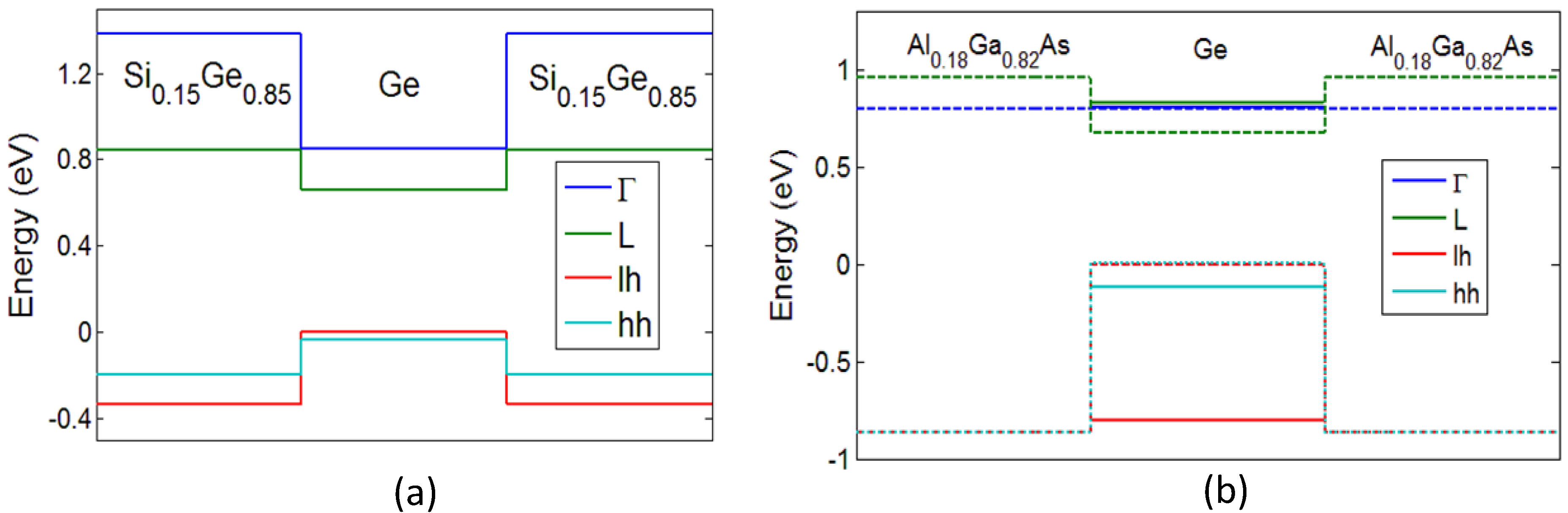
In addition to directly engineering the Ge material itself, we proposed that the band structure of Ge could also be engineered towards direct gap semiconductor by carefully designing the QW device structures [55]. QWs are commonly applied in LDs to reduce the threshold current density and increases quantum efficiencies. Theoretical investigations on direct gap Si/Ge superlattices and QWs have started since 1980s [56] and have continued through recent years [57,58]. However, there has been no experimental demonstration of direct gap SiGe QW structures so far. A couple of challenges have to be addressed. Firstly, in SiGe/Ge QWs the quantum confinement actually increases the energy difference between the direct and indirect gaps due to the much smaller effective mass and much stronger confinement of Γ electrons, as shown in Figure 4a. Secondly, the epitaxial growth of Ge on SiGe typically results in compressive strain in Ge due to the lattice mismatch, which also increases the energy difference between Γ and L valleys.
In order to improve the Ge QW structures, we proposed a “separate electron barrier” approach [55], where the barrier material provides strong confinement in the L valleys, but weak confinement in the Γ valley. This idea can be implemented by carefully choosing the barrier material that provides a large band-offset in L valleys while small offset in Γ valley with Ge (Figure 4b). Such band alignment can make Ge “direct band gap” by raising the L valleys above the Γ valley due to the stronger quantum confinement of electrons in the L valleys. As an example, the band diagram of an AlGaAs/Ge/AlGaAs QW structure is shown in Figure 4b, where the Ge QW is converted into a direct gap semiconductor due to the stronger quantum confinement of electrons in the indirect L valleys provided by the AlGaAs barriers. One could also tweak the design to engineer the L valley slightly below the Γ valley for high lasing performance at elevated temperatures. There are several advantages of this approach: (1) The AlGaAs barrier layer is not an active material but just a barrier layer electrode, so it can be deposited at low temperature to avoid diffusion of III and V elements and achieve CMOS compatibility. (2) Off-cut wafers may not be needed either, since antiphase boundaries will not significantly affect the performance in this case. (3) Pseudo-direct gap Ge lasers offer much better thermal stability, and in this case one can engineer the relative positions of L and Γ valleys by QW design for optimal performance. In III-V lasers, quantum dot (QD) lasers also show good thermal stability, but the wavelength of these QDs is far from 1550 nm and they have not been integrated on Si so far. Therefore, this new Ge QW design could offer a simple solution to high-performance monolithic lasers on Si at 1500–1700 nm. In the case of tensile strained Ge or GeSn active gain media, the energy gap reduction due to tensile strain and/or Sn alloying can also be partially compensated by the quantum confinement effect. This compensation helps to avoid potential issues related to the dark current in small band gap semiconductors.
Figure 4.
(a) Ge0.85Si0.15/Ge/Ge0.85Si0.15 QW band structure assuming 0.25% tensile strain in an 11.8 nm thick Ge QW. (b) Band structures of an AlGaAs/Ge/AlGaAs QW for separate electron confinement in L and Γ valleys assuming no strain (due to nearly perfect lattice matching). The thickness of Ge is 3.3 nm. For different valleys, dashed lines show the band edges and solid lines show the first energy level in the wells. Barrier material is chosen so that there is little quantum confinement in Γ valley but significant confinement in L valley. © 2013 IEEE. Reprinted, with permission, from [55].

In summary of this section, our analyses show that it is highly feasible to achieve direct gap or optimized pseudo-direct gap Ge-based active photonic devices on Si by leveraging tensile strain, Sn alloying, n-type doping, as wells as separate confinement of L vs. Γ electrons in QW structures.
3. Ge and GeSn Growth on Si
To implement the band engineering approaches mentioned in Section 2, high quality Ge and GeSn growth on Si is the first critical step. The greatest challenge for high quality Ge epitaxy on Si is the 4.2% lattice mismatch between these two materials. In this section, we will discuss both epitaxial growth and recent investigations towards low-temperature growth of high crystallinity Ge and GeSn on amorphous dielectric layers for 3D photonic integration.
3.1. Epitaxy
Epitaxy is the most common approach to grow Ge on Si. To achieve device quality epitaxial Ge on Si without using very thick SiGe buffer layers, a two-step direct Ge growth technique has been applied to prevent Stranski–Krastanov growth [59,60] and subsequent annealing has been developed to decrease the threading dislocation (TD) density below 107 cm−2 [61]. In the initial growth step, a thin epitaxial Ge buffer layer of 30–60 nm is directly grown on Si at 320–360 °C. At such a low growth temperature islanding of Ge associated with Stranski–Krastanov growth is kinetically suppressed due to the low surface diffusivity of Ge. In the second growth step, the growth temperature is increased to >600 °C for higher growth rates and better crystal quality. A post-growth annealing at >750 °C can reduce the TD density from 109 to 107 cm−2. It has also been shown that the TD density decreases with the increase of Ge film thickness [62], similar to the case of GaAs epitaxy on Si [63]. Luan demonstrated that the TD density could be reduced to 7.9 × 106 cm−2 for a 3.9 μm-thick Ge layer [62]. This phenomenon can be well explained by a dislocation coalescence/annihilation model during the epitaxial growth or annealing [63,64]. More recently, a low threading dislocation density of 1.3 × 106 cm−2 has been demonstrated in blanket Ge-on-Si films by growing a 4.5 μm-thick Ge layer and etching it back to 1.8 μm [65]. In selectively grown Ge mesas with lateral dimensions ~10 μm, the average TD density can also be reduced to low 106 cm−2 even for a relatively thin film of 1 μm [61,62] because these dislocations can glide to the edge of the mesas and annihilate. This selective growth method is more efficient than the growth of thick blanket Ge layers and more compatible with photonic device integration. Details about the two-step growth and dislocation reduction methods can be found in some recent reviews [66,67,68]. In particular, in-situ n-type doping methods have been reviewed in [66,67]. In CVD process, a phosphorous doping level up to 5 × 1019 cm−3 has been achieved by depositing a stack of delta-doped Ge layers at low temperatures on top of regularly in-situ doped Ge (with n = 1–2 × 1019 cm−3) followed by drive-in annealing [69,70]. These materials enabled the first demonstration of band-engineered Ge-on-Si LDs. To accommodate the thermal budget for epitaxial growth in device integration, the Ge epitaxy is commonly performed after the gate formation but before the metallization process (see the processing temperature color bar in Figure 1).
Epitaxy of GeSn has been implemented by both MBE and CVD. The development of SnD4 precursor was the key factor that enabled Sn alloying in CVD growth [71]. The deposition temperature is typically between 200 and 350 °C, and higher Sn content typically requires lower growth temperature to prevent Sn segregation. Compared to Ge, GeSn tends to relax more easily on Si substrate due to an even larger lattice mismatch. Similar to epitaxial Ge, annealing has been shown to improve the optoelectronic properties of GeSn [45,72] by reducing the defect density. Rapid thermal annealing (RTA) is preferred in this case to remove the defects without causing Sn segregation. Since room-temperature light emission has been demonstrated from both MBE and CVD growth samples, there does not seem to be significant difference in material quality between these two epitaxial growth methods.
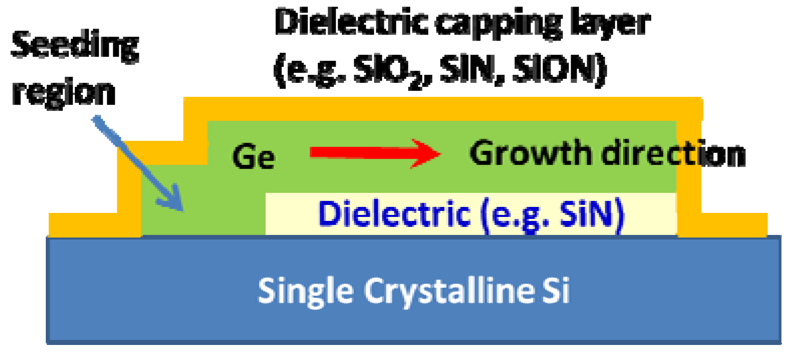
In recent years, the rapid melting growth (RMG) or liquid phase epitaxy (LPE) of Ge has been developed as an alternative to MBE and CVD epitaxy [73,74,75]. A typical Ge RMG/LPE structure is schematically shown in Figure 5. An amorphous Ge (a-Ge) thin film is deposited on a dielectric layer, with a small window in contact directly with the single crystalline Si substrate or a patterned Si grain to serve as the seedling region for the single crystal Ge growth upon melting and recrystallization. The a-Ge deposition does not require MBE or CVD epitaxy tools, so it can be implemented by less costly, higher throughput methods such as plasma enhanced CVD (PECVD). In some cases, a very thin SiGe buffer layer is deposited first to reduce the columnar growth and the surface roughness [75]. A dielectric capping layer such as SiO2 is often deposited on top of the a-Ge before the RMG process. Since a high temperature >937 °C is required to melt Ge, RMG has to be incorporated into the front-end-of-line (FEOL) processing during device integration, along with the RTA for activating implanted dopants in the source/drain regions [75]. Upon melting at ~1000 °C, the Ge crystal grows laterally, seeded by the region in contact with single crystal Si. The key to this approach is to achieve a fast lateral growth rate to prevent random nucleation of Ge grains on the dielectric layers. Experimental results have consistently shown that the single crystal regime can sustain for tens to hundreds of microns, large enough for integrated Ge photonic and electronic device fabrication. Since the defects due to Si/Ge lattice mismatch is confined to the seed region, nearly defect-free single crystalline Ge strips can be obtained away from this seeding region. Indeed, a high hole mobility of >1000 cm2 V−1 s−1 has been reported [74], indicating a high material quality. Recently, a thermally induced tensile strain of 0.4% has been reported from Ge-on-insulator grown by RMG [76] due to the high growth temperature and reduced stress relaxation upon rapid cooling after RTA. One of the challenges for photonic applications, though, is that the Ge region almost inevitably incorporates a small amount of Si due to Ge-Si inter-diffusion upon melting. Incorporation of Si tends to blue-shift the direct band gap and increases the difference between the direct and indirect gaps. For PDs, the blue-shift will affect the optical absorption at longer wavelengths (λ > 1550 nm). For EAMs and LDs, the performance tends to deteriorate due to the increase in the energy difference between the direct and indirect band gaps.
Figure 5.
Schematics of a typical structure for Ge RMG/LPE growth. A cross-sectional view is shown here.
Figure 5.
Schematics of a typical structure for Ge RMG/LPE growth. A cross-sectional view is shown here.

3.2. Growth Methods towards 3D Photonic Integration
So far, most of the Ge photonic devices are grown on single-crystal Si (either SOI or Si substrate) via heteroepitaxy, constituting a planar integration scheme (Figure 1c). However, heteroepitaxy of Ge consumes device area on single crystal Si, thereby significantly sacrificing CMOS area for photonic devices. The size of the photonic devices is limited by the diffraction as well as the optical path length necessary for light-matter interaction. For example, a waveguide-integrated Ge PD is typically >0.1 μm2 in cross-section and from several microns to tens of microns in length. This footprint is more than 100× larger than CMOS transistors in 22 nm technology node. Furthermore, this planar integration approach has to introduce some modifications to existing CMOS process flow in order to accommodate the epitaxial growth as well as the vertical dimension of photonic devices (typically several hundred nm thick). These modifications are hard to implement in <45 nm CMOS technology nodes. Therefore, for large-scale EPICs it would be ideal to adopt a 3D configuration, moving the photonic circuits to the metal/dielectric interconnect level above the CMOS layer using BEOL processing. For monolithic 3D photonic integration, the major challenges for materials growth are: (1) the lack of single crystal template for epitaxy makes it difficult to achieve high crystallinity; and (2) the processing temperature has to be kept below ~500 °C to be compatible with the metal contacts. Although metal induced crystallization (MIC) has been investigated to achieve low crystallization temperature [77,78,79], the metals commonly used in MIC, including Ni, Au, Co, Ag, Pd and Al, either introduce deep-level defect centers or exceedingly high doping concentrations that are detrimental to semiconductor device performance [80]. On the other hand, direct growth of Ge or GeSn on amorphous dielectric layers also offers a new opportunity in that the constraint of lattice mismatch in epitaxy is naturally removed. Once implemented, it offers unprecedented flexibility in fabrication of 3D circuit structures.
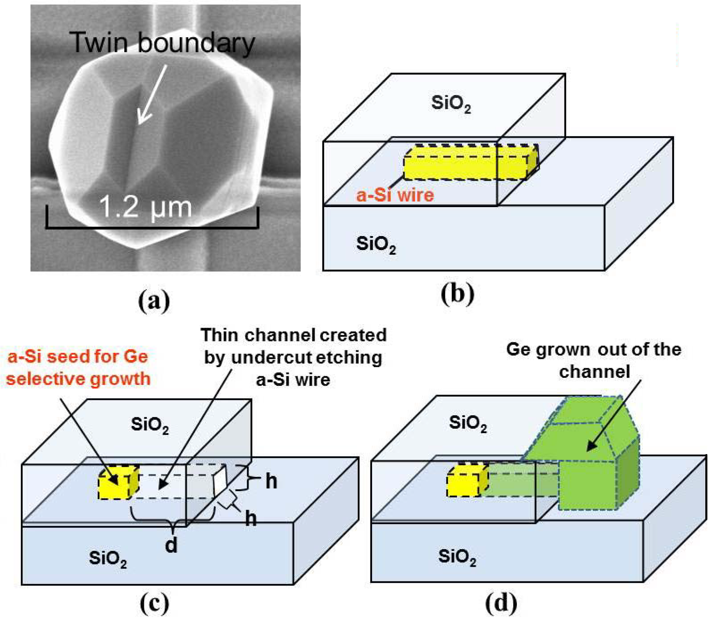
To grow single crystalline Ge on amorphous dielectric layers, we have proposed and demonstrated the concept of geometrically-confined growth of single crystalline Ge on amorphous Si at a low growth temperature of 450 °C, as shown in Figure 6 [81]. The facets of the Ge material in Figure 6a indicate the single-crystal nature of the grain. The observed boundary (also confirmed by electron backscatter diffraction, EBSD) is a coherent interface with no dangling bonds to cause mid-gap states, so it will not adversely affect the optoelectronic properties. To achieve geometrical confinement for Ge growth, we first fabricate ~200 nm-wide amorphous Si (a-Si) wires on a SiO2 layer, then cover them with another SiO2 layer and etch from the top to expose one end of the Si wires (Figure 6b). An undercut etching of the a-Si wire using TMAH forms a hollow channel for geometrical confinement (Figure 6c). During the ultrahigh vacuum CVD (UHVCVD) process, Ge only selectively deposits on Si but not on SiO2. Therefore, in this geometric configuration Ge growth has to start from the a-Si seed with a nanoscale cross-section of ~200 × 200 nm2 and propagate laterally along the channel. Multiple Ge nuclei may start to form on the a-Si seed initially, leading to a growth competition of Ge grains inside the channel. During this competition, the nucleus with the fastest lateral growth rate along the channel will eventually dominate and block the growth of other grains if the aspect ratio of the channel, d/h, is large enough. This nucleus typically has its <110> orientation aligned with the channel, the fastest growth direction in Ge considering the effect of twinning. Therefore, the fastest-growing grain is selected by the geometric confinement and leads to single crystal Ge growth outside the channel (Figure 6d). Using this geometrically confined growth method, in principle the area of the single crystal Ge region can be enlarged to any desirable size simply by increasing the growth time. However, in reality the lateral growth rate is limited to a few μm/h in order to prevent random Ge nucleation on the SiO2 mask layer. In addition, the shape of the Ge single crystal is hard to control exactly.
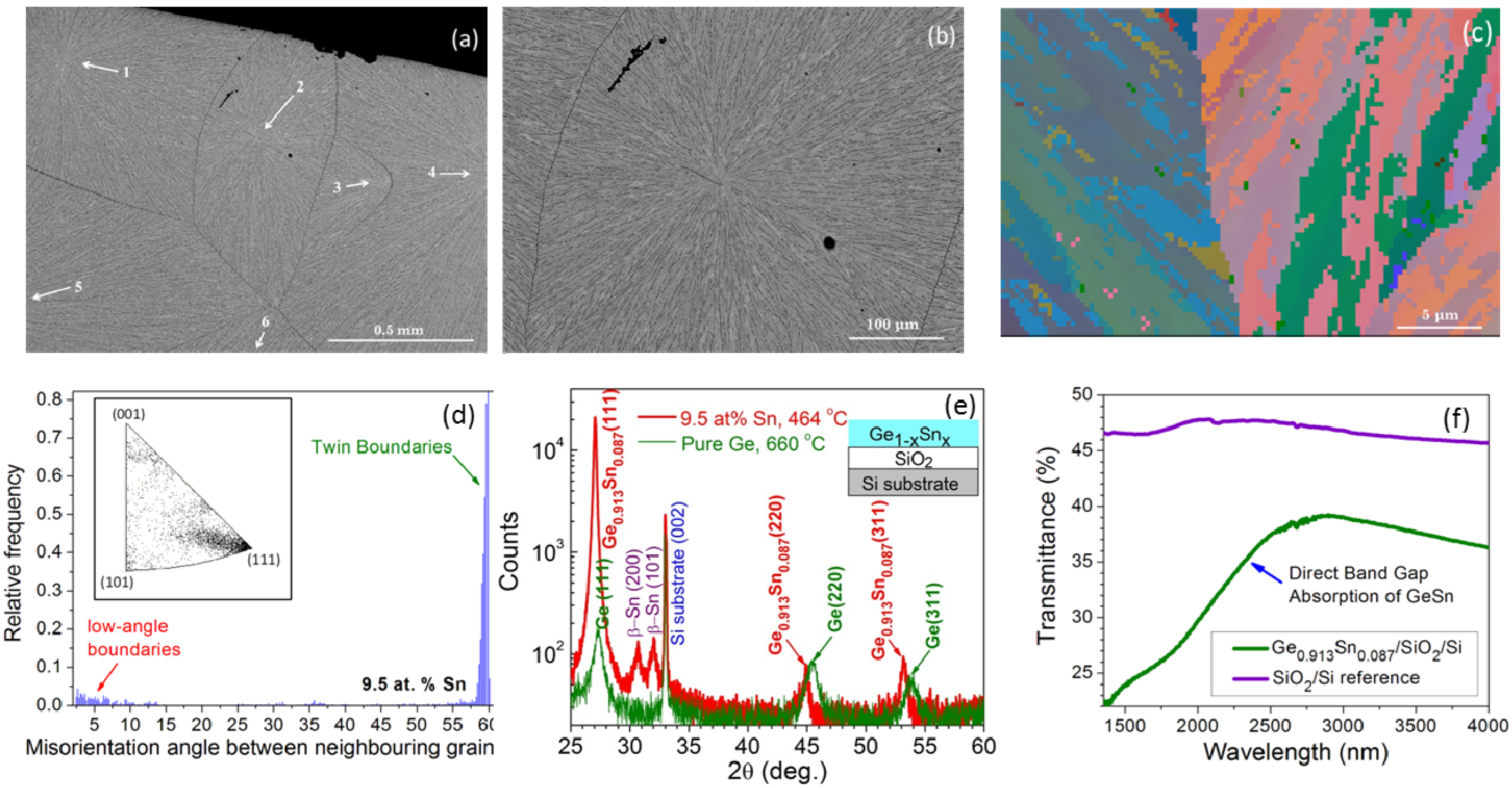
Considering that Sn and Ge form a eutectic system with a low eutectic temperature of 231 °C, we expected that the GeSn alloy may crystallize at a lower temperature with a higher lateral growth rate than Ge. As mentioned earlier, Sn alloying also enhances the optoelectronic properties by transforming Ge towards a direct gap semiconductor. Therefore, recently we studied the crystallization of GeSn on amorphous SiO2 layers towards monolithic 3D photonic integration [47]. Amorphous GeSn (a-GeSn) films were evaporated on a layer of SiO2 followed by crystallization annealing. The eutectic phase transition in Ge-Sn system greatly enhances the crystallization at <500 °C. Pseudo-single-crystalline GeSn thin films with up to 8.7 at % Sn has been directly grown on a SiO2 layer at ~460 °C. As shown in Figure 7a,b, we clearly identified nucleation centers that are as far as ~0.1–1 mm away from one another, from which the grains grow radially. This striking observation is highly unusual in the crystallization of amorphous semiconductor thin films, and it suggests an extraordinarily fast lateral grain growth rate vs. a slow nucleation rate during the eutectically enhanced crystallization process of GeSn. EBSD analysis shows that the average grain size is as large as ~10 μm, and the majority of grain boundaries are relatively benign twin boundaries (Figure 7c,d). For an initial Sn composition of 9–13 at % in the as-deposited films, the crystallized GeSn film exhibits a strong (111) texture, as shown by the inverse pole figure in the inset of Figure 7d and the X-ray diffraction (XRD) data in Figure 7e. We also found that the excess Sn segregates on the surface of the GeSn thin films along the small angle grain boundaries, and it can be selectively removed by a 37% HCl:H2O solution with a high Sn-to-GeSn (Ge-rich) etching selectivity >4800:1 [47]. After the selective etching, β-Sn signals no longer exist in the XRD data. From XRD, micro-Raman, energy dispersive X-ray spectroscopy (EDS) and EBSD analyses, it was found that the films exhibit ~0.3% tensile strain and 8.7 at % substitutional Sn composition. Similar to the cases of MBE and CVD, the substitutional Sn composition far exceeds the equilibrium solubility of Sn in Ge (~1 at %). Moreover, the substitutional incorporation of 8.7 at % Sn into Ge and the 0.3% tensile strain transform the material into a direct gap semiconductor. As mentioned in Section 2, the measured band gap of ~0.5 eV from optical transmittance spectroscopy (Figure 7f) is in good agreement with the theoretical calculation in Figure 3. Further employing geometrically confined growth, it is promising to achieve single crystalline GeSn on dielectric layers for high-performance active devices in 3D photonic integrated circuits.
Figure 6.
(a) Top view scanning electron microscopy (SEM) photo of a single crystal Ge grain grown on a SiO2 layer using geometric confinement method. The fabrication steps for the geometrically confined Ge growth are shown in (b–d). Reproduced from [81] with permission from McComber, K.; Duan, X.; Liu, J.F.; Michel, J.; Kimerling, L.C.; Advanced Functional Materials; published by John Wiley & Sons, 2012.

Figure 7.
(a) Large-area SEM image of a Ge0.913Sn0.087 thin film crystallized from a-GeSn with 9.5 at % Sn. The arrows point to six nucleation centers in a total area of ~1.6 mm2, from which GeSn grains grow radially. The scale bar is 0.5 mm. (b) A zoomed-in image of domain 2 in (a). The scale bar is 100 μm. (c) EBSD mapping of the crystallized GeSn thin film, where different colors indicate different in-plane crystallographic orientations. The scale bar is 5 μm. (d) Distribution of misorientation angles between neighboring grains derived from the EBSD data. The inset shows the inverse pole figure obtained over a 0.2 × 0.2 mm2 area, indicating a strong (111) texture. (e) θ-2θ XRD data of the GeSn sample vs. a pure Ge sample. The GeSn sample shows a strong (111) texture, confirming the EBSD result. Note that the vertical axis is in log scale. (f) Transmittance spectrum of the high crystallinity Ge0.913Sn0.087 thin film sample compared to a reference sample without the GeSn thin film. The onset of strong absorption at ~λ = 2500 nm is consistent with the calculated direct band gap of ~0.5 eV. Reproduced from [47] with permission from the Optical Society of America under the Author’s Copyright Transfer Agreement.

4. Ge-on-Si Active Photonic Devices
Armed with high quality Ge materials on Si, high performance Ge-on-Si PDs and EAMs have been demonstrated in recent years. Prototype Ge-on-Si LDs have also been achieved. In this section, we will first discuss waveguide-coupling schemes for integrated Ge photonic devices on Si. We then discuss each Ge-on-Si active photonic device individually.
4.1. Waveguide Integration Schemes
Waveguide-coupling with Ge active photonic devices is indispensable to construct integrated photonic circuits. Butt-coupling and evanescent coupling are the most commonly used waveguide-coupling schemes, as schematically shown in Figure 8.
Figure 8.
Schematic structures of typical waveguide-integrated Ge active photonic devices. (a) butt-coupled; (b) Evanescent coupling with waveguide at the bottom of the Ge photonic device; (c) Evanescent coupling with waveguide on top of the Ge photonic device [18].
Figure 8.
Schematic structures of typical waveguide-integrated Ge active photonic devices. (a) butt-coupled; (b) Evanescent coupling with waveguide at the bottom of the Ge photonic device; (c) Evanescent coupling with waveguide on top of the Ge photonic device [18].
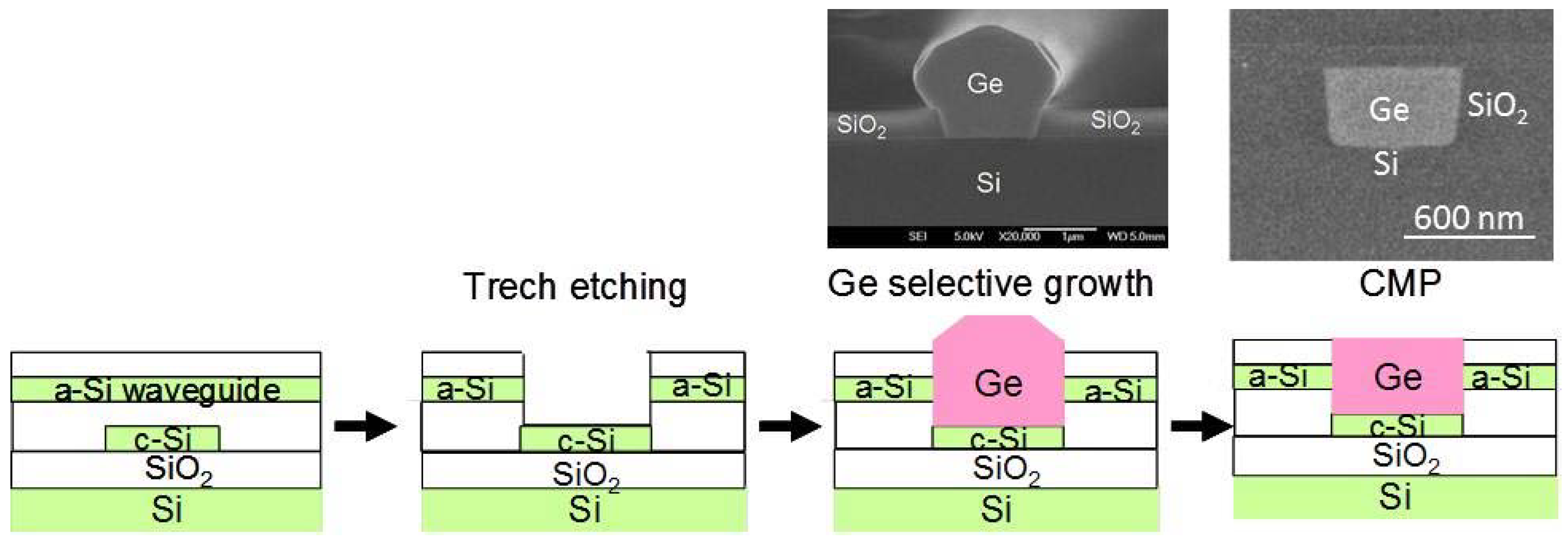
Butt-coupling launches optical power directly into the Ge active device region, thereby offering a higher coupling efficiency compared to evanescent coupling in most cases. It is also straightforward to couple the light into and out of the Ge or GeSi region for EAMs. Therefore, the same butt coupling structure can be applied to all Ge active photonic devices for monolithic photonic data links [82,83]. The fabrication process of butt-coupled devices is typically more elaborate than evanescently coupled ones, though, since Ge has to be selectively grown to fill pre-defined trenches in order to implement butt-coupling structures [83,84,85,86,87]. Chemical mechanical polishing (CMP) is often required to flatten the top of the Ge mesas since single crystalline selective growth usually results in faceting and a non-planar surface. An example of such a fabrication process is schematically shown in Figure 9, where cross-sectional SEM images of Ge overgrown out of the trench and after planarization are also presented.
Figure 9.
Schematic fabrication process of butt-coupled Ge PDs and EAMs on SOI platform. “a-Si” and “c-Si” refer to amorphous Si and crystalline Si, respectively. Trench-filling selective growth is applied to achieve these structures. Cross-sectional SEM pictures of trench-filled Ge selective growth and the Ge region after CMP are also shown. © 2006 IEEE. Reprinted, with permission, from [88].

Several types of butt-coupling structures have demonstrated high coupling efficiencies. For example, the Ge PD/EAM has been designed and fabricated as a segment of the waveguide, with its dimensions optimized for maximum modal overlap with that of the input and output Si waveguides [83,84]. Tapered mode converters have been applied to enhance butt-coupling efficiency [86]. To enhance the tolerance to fabrication errors, especially lateral misalignment, in some cases a wide patch of Ge is used to capture the optical power coupled and scattered into the Ge region [85]. This kind of optical design is somewhat similar to multi-mode interference (MMI) couplers. It could be extended to EAMs if output coupling is also designed carefully to distribute the modulated light into different channels. The trade-off is that the Ge device area tends to be large.
Evanescent coupling uses the fact that light can be easily coupled evanescently from a lower index material (i.e., waveguide) to a higher index material (e.g., Ge PDs) as long as the index difference is small enough. The electromagnetic mode and hence the optical power is typically transferred gradually to the high index material. The waveguide is usually placed either on bottom or on top of the Ge region to simplify fabrication processes. In bottom-waveguide-coupled structures, Ge devices are typically grown epitaxially on crystalline Si waveguides fabricated on SOI substrates. By comparison, top-waveguide-coupled structures allow greater flexibility in choosing waveguide material since they do not have to form a template for Ge epitaxy. The waveguide material can be amorphous, such as amorphous Si (a-Si), SiON or SiN. These amorphous waveguides are applicable to photonic circuits at the upper interconnection level for 3D photonic integration.
Ahn et al. [89,90] systematically studied evanescent coupling processes between the waveguide and the Ge active region in the case of Ge PDs, which can be readily extended to other waveguide-coupled Ge devices since the coupling only depends on the refractive index profile and the geometry. The analysis identified three mechanisms: (i) Direct coupling and scattering into the Ge region due to mode matching and abrupt effective index change (Figure 10a); (ii) Evanescent coupling at a constant rate (Figure 10b); and (iii) Backscattering of residual optical power in the waveguide into Ge at the end of waveguide/Ge coupling region due to the abrupt change in effective index and geometry. Most waveguide-coupled Ge PDs are designed to absorb all input photons, so Mechanism (iii) is negligible in most cases since there is hardly any residual optical power in the waveguide at the end of the coupling region. However, this factor needs to be taken into account for EAMs since optical output from the Ge active region is also important. Mechanism (i) is more efficient than Mechanism (ii) in coupling optical power into the Ge region, so it is the preferred mechanism for waveguide-coupled Ge PDs. On the other hand, Mechanism (ii) is similar to directional couplers and can be adapted to waveguide-coupled GeSi EAMs. In this case, the light oscillates between the input waveguide and the EAM active region for optical modulation before it exits the output port of the waveguide [91]. Ahn et al. also investigated two major factors that affect coupling efficiency for vertical evanescent coupling in Ge PDs: (1) The refractive index difference between Ge and the core of the waveguide materials, nGe-ncore; and (2) The geometrical factor of the waveguide. Generally speaking, low index difference between the waveguide and the Ge region, small cross-sectional dimensions of the waveguides, and low height-to-width aspect ratio of waveguides lead to a Mechanism (i) dominated regime and greatly enhanced coupling efficiency into Ge. Lower index differences reduce the impedance mismatch between the waveguide and the Ge region, thereby facilitating coupling. Smaller waveguide cross-sectional dimensions or aspect ratio help to increase optical confinement in the Ge region for more efficient optical absorption. In some device structures, thick Si waveguides is preferred for optimal performance, such as waveguide-coupled avalanche photodiodes (APDs). To enhance evanescent coupling efficiency between thick Si waveguides and Ge APDs, we have designed a step coupling structure to create mirror imaging modes at the Ge/Si interface using a vertical MMI mechanism [92]. The coupling length has been effectively reduced by 5× for 70% absorption, and 3× for 90% absorption.
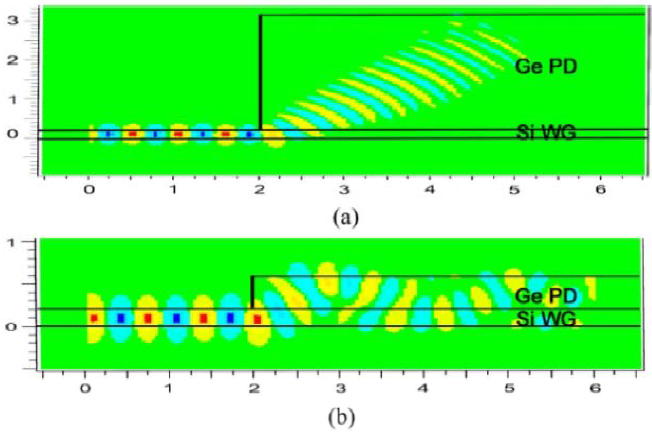
Figure 10.
3D finite difference time domain (FDTD) simulation of photon propagation in bottom-waveguide-coupling structures (a) 3.0 μm vs. (b) 0.4 μm thick Ge active region is placed on 0.2 μm thick Si channel waveguide. Ge absorption coefficient of αGe = 4000 cm−1 at λ = 1550 nm was assumed for simulation, i.e., considering 0.22% tensile strain in Ge. As shown in the figures, when the thickness of the Ge region decreases relative to the Si waveguide, the coupling efficiency deceases due to a shift in coupling mechanism from direct coupling and scattering dominated regime (Mechanism i) to evanescent coupling at a constant rate (Mechanism ii). The unit of the axes is micron. © 2010 IEEE. Reprinted, with permission, from [89].

4.2. Ge-on-Si PDs
Ge-on-Si PDs are the most mature integrated Ge photonic devices. Most of them adopt a p-i-n diode structure, with the intrinsic layer being Ge and at least one of the p/n electrodes being heavily doped Si substrate [93,94,95]. The key to high performance devices is to optimize the built-in field in the intrinsic Ge region so that carriers can be collected fast enough before recombining at any defect centers. For high quality intrinsic epitaxial Ge layers, full responsivity can be achieved even at 0 bias (photovoltaic mode) due to this large built-in electric field [93]. Free-space coupled Ge-on-Si p-i-n photodiodes have reached a bandwidth of 49 GHz at −2 V reverse bias [96]. The dark current density has been reduced from ~10 mA/cm2 to ~1 mA/cm2 at −1 V over the past decade mainly by improving the surface passivation to decrease peripheral leakage for devices with small dimensions ≤100 μm2 [97]. Note that reducing the device area also decreases RC delay and increases the bandwidth of the device. As mentioned in Section 3.1, in these small area devices, the TD density is much lower than in blanket films, so the dark current is dominated by generation-recombination at the Ge/passivation interface. When the passivation interface is properly doped or treated, the depletion region is pushed away from the passivation interface, thereby reducing the generation/recombination current. Based on the same consideration, the low-quality Ge buffer layer mentioned in Section 3.1 is heavily doped either by drive-in diffusion from the Si substrate during the post-growth annealing [62] or via in-situ doping [98]. The Ge buffer layer now becomes part of the electrode so that the incorporated misfit dislocation network does not contribute significantly to generation/recombination. By now, the performance of free-space Ge-on-Si p-i-n diodes is comparable to their III-V counterparts at 850 and 1310 nm. The responsivity at 1550 nm is usually a bit lower than InGaAs detectors due to a lower absorption coefficient. This is mainly because the direct band gap of 0.2% tensile strained Ge (0.77 eV) is larger than InGaAs (≤0.75 eV). With the recent progress in band engineering methods described in Section 2, it is possible to further improve the responsivity at 1550 nm for free-space Ge-on-Si PDs, e.g., by increasing tensile strain or incorporating a small amount of Sn. Indeed, recently a 40 GHz Ge0.98Sn0.02 free-space p-i-n photodiode has been demonstrated [99] with the responsivity at 1550 nm 2× higher than a pure Ge photodiode of the same absorber layer thickness. In 2011, commercial optical receivers based on free-space Ge-on-Si PDs monolithically integrated with Si trans-impedance amplifier (TIA) circuits were reported by Analog Devices, Inc. [100]. Data rate up to 43 Gb/s was demonstrated from vertically illuminated Ge-on-Si receivers recently [101]. Free-space Ge-on-Si APDs, which synergistically integrate the high absorption of Ge layers at telecommunication wavelengths with the outstanding low-noise avalanche gain in Si, have demonstrated performance superior to their III-V counterparts [102] and are being commercialized for 10G-PON applications [103].
To achieve photonic circuits on Si, waveguide-integrated Ge-on-Si PDs have been developing rapidly in recent years. An additional benefit for device performance is that they have no trade-off between bandwidth and quantum efficiency as do free-space PDs [88,104,105]. This is because in waveguide-integrated PDs, the optical absorption path is in the longitudinal direction along the waveguide, which can be as long as needed to fully absorb the input optical power. On the other hand, carrier collection can be implemented in a transverse direction perpendicular to the light propagation direction, with a dimension in the order of several hundred nm to minimize carrier transit time and increase bandwidth. One can optimize the PD design for maximum bandwidth while maintaining a high quantum efficiency >90%. Since the first reports on waveguide-integrated Ge-on-Si PDs, the performance of these devices has been rapidly improving. Table 1 summarizes the reported performance of waveguide-coupled Ge-on-Si PDs since 2009 (the data between 2006 and 2009 have been summarized in [68]). The responsivity is typically ~1 A/W at λ = 1550 nm, or >80% quantum efficiency. The bandwidth has generally exceeded 40 GHz since 2009 [75,85,106]. A 60 GHz evanescently coupled Ge p-i-n diode has been demonstrated very recently by coupling the detector with a carefully designed inductor-capacitor circuit utilizing inductive gain peaking [107]. An estimated bandwidth of 120 GHz has been reported in [108] with the directly measured result exceeding 67 GHz. The maximum bandwidth-efficiency product has exceeded 30 GHz [86,108]. In selectively grown butt-coupled Ge photodetectors with sidewall passivation by PECVD SiO2, a low dark current density of 0.7 mA/cm2 at −1 V has been achieved with a very small absolute dark current of 0.2 nA [84]. This absolute dark current is orders of magnitude lower than typical free-space diodes. However, in some literature a large dark current density was reported [86,108]. Considering the high responsivity and bandwidth of these devices, it is likely that Ge material itself is still of high quality, and the leakage is mainly due to peripheral passivation issues. In terms of system integration, Kotura, Inc. recently reported terabits/s wavelength division multiplexing (WDM) photonic receiver chips based on 40 waveguide-coupled Ge-on-Si PDs monolithically integrated with a 40-channel WDM echelle grating [109]. For Ge-on-Si APDs utilizing avalanche gain in the Si layer, waveguide integration can at least double the primary responsivity compared to free-spaced ones, which further improves their sensitivity [92,110]. Photocurrent gain from the Ge region itself has also been utilized to enhance the sensitivity of waveguide-coupled PDs [111].

Table 1.
Summary of waveguide-coupled Ge-on-Si PD performance. All devices are fabricated by epitaxial growth on Si and performance data are reported for −1 V reverse bias, unless otherwise stated.
| Responsivity (A/W) @ 1550 nm | 3dB Bandwidth (GHz) | Dark Current Density (mA/cm2) | Absolute Dark Current (μA)@ −1 V | Device Design | Reference | ||
|---|---|---|---|---|---|---|---|
| Max | 0 bias | Max | 0 bias | ||||
| 1.1 | - | 37@−3 V | 17.5 | 1.6 × 10⁴ | 1.3 | butt p-i-n | [86] |
| 1@-4 V | 0.2 | 42@−4 V | 12 | 60 | 0.018 | butt p-i-n | [85] |
| >1.1 @ <1540 nm | - | 50@−5 V | - | 8900@ −5 V a | 4@−5 V | Bottom msm | [106] b |
| 0.42 | 0 | 40@−2.5 V | - | - | 90 | bottom msm | [75] c |
| 0.95 | - | 36 | - | 29 | 0.0046 | bottom p-i-n | [112] |
| 0.8 | 0.78 | >67; estimated 120 | 40 Gb/s | 8 × 10⁴ | 4 | butt | [108] |
| 0.75@−2 V | - | 60@−2 V | - | 3750 | 3@−2 V | bottom p-i-n | [107] |
a Calculated and/or read from corresponding figures of the reference. b Ge layer fabricated by wafer bonding. c Ge layer fabricated by rapid melt growth (RMG).
In recent years, bandwidths at 0 bias (photovoltaic mode) have also been improved significantly especially for waveguide-integrated p-i-n PDs. This is because the thickness or width of the intrinsic Ge region can be reduced to obtain a stronger built-in electric field at 0 bias without affecting the optical absorption path length in the longitudinal direction. Full responsivity and up to 40 Gb/s data rate have been demonstrated at 0 bias [108]. Operations under photovoltaic mode at 0 bias are especially beneficial to achieve high energy-efficiency in large-scale EPICs since the PDs practically consume no power at all. One could even consider harvesting electrical power directly from the incident laser by operating the Ge PDs under photovoltaic mode. For example, the photovoltage could be used to drive electronic circuits without using power consuming TIA circuits. The energy conversion efficiency can also be much higher than solar photovoltaic cells, since the optical power from the laser is at a single wavelength. Using the demonstrated dark current density of 1 mA/cm2 and responsivity of 1.1 A/W at 1550 nm, under 100 nW optical input an 0.5 × 10 μm2 waveguide-coupled Ge PD would offer an open circuit voltage of ~0.2 V. Considering that the driving voltage of CMOS in 22 nm technology node has been decreased to ~0.8 V, 4 Ge PDs in series are enough to provide the driving voltage for CMOS circuitry, potentially eliminating the need for TIAs and minimizing the energy consumption in EPICs.
4.3. Ge and GeSi EAMs
Similar to III-V semiconductors, the direct gap absorption in Ge can be effectively modified by an applied electric field, known as electroabsorption (EA) effect. EA effect in semiconductors include Franz-Keldysh effect (FKE) in bulk materials and quantum-confined Stark effect (QCSE) in QW structures.
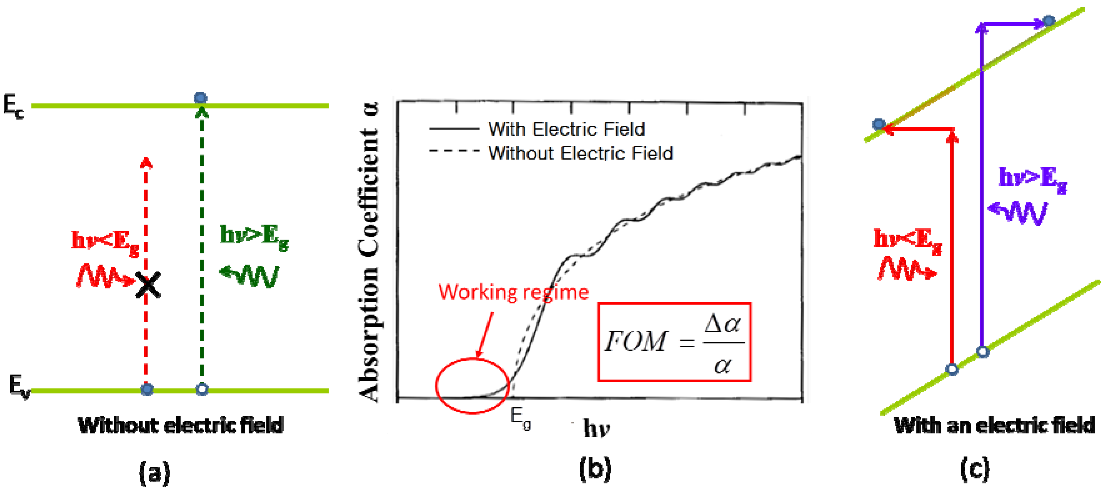
Figure 11 schematically shows the optical absorption process and absorption spectra in a semiconductor material with and without an electric field. Without the field, photons with energy less than the band gap are not absorbed, while those with energy above the band gap are (Figure 11a). The absorption coefficient spectrum follows the well-known square-root relation for direct gap transitions (Figure 11b, dashed line). With an applied field, the absorption process can be considered as band-to-band tunneling under photon excitation. In this case, even a photon with hν < EgΓ can excite an electron from the valence band to the conduction band through a cooperative tunneling process across a triangular energy barrier (Figure 11c). Therefore, the absorption coefficient at hv < EgΓ increases compared to the case without the electric field. On the other hand, for hv slightly greater than EgΓ the absorption curve shows oscillating behavior near the band edge, known as Franz-Keldysh oscillations (Figure 11b, solid line). This is due to the fact that, for excited electrons with energy slightly greater than the triangular barrier, the probability to cross the barrier and reach its final state on the tilted conduction band edge is determined by the interference between the electron wavefunction and the barrier. This phenomenon is well known in quantum tunneling and it is similar to the Fabry-Perot oscillations in optics, both resulting from the nature of waves. While the picture presented above is simplified, it does capture most of the physics in FKE [113].
Figure 11.
(a) Schematics of band-to-band optical absorption in a bulk semiconductor material without an applied electric field. (b) Absorption spectra of the material with and without an electric field. (c) Schematics of absorption process in a bulk semiconductor material under an applied electric field (Franz-Keldysh effect).

In QWs, the binding energy of excitons is notably larger than in bulk materials due to the quantum confinement, so exciton absorption peaks are clearly visible even at room temperature. Therefore, in addition to band-to-band transitions, the significant exciton absorption peak will notably enhance the EA effect compared to bulk materials. A rigorous, quantitative analysis of FKE and QCSE can be found in [114]. It is noteworthy that the stronger the optical absorption (without electric field), the stronger the EA effect since both are proportional to the transition matrix element between the valence band and the conduction band. As a result, only direct gap transitions show significant EA effect.
The figure-of-merit (FOM) for EAM materials and devices is the absorption contrast, Δα/α, i.e., relative change in absorption coefficient when an electric field is applied. As shown in Figure 11b, this is maximized at photon energies slightly smaller than the direct band gap. While FKE in bulk Ge only shows a Δα/α ~ 1 mainly limited by background absorption associated with indirect gap transition, 0.2% tensile-strained Ge demonstrates a significantly better absorption contrast of Δα/α ~ 4 at λ ~ 1630 nm since the energy difference between direct and indirect gaps is decreased [115]. On the other hand, strong QCSE from the direct gap transition of Ge has been demonstrated in strain-balanced Ge/Si0.15Ge0.85 multiple QWs grown on a relaxed Si0.1Ge0.9 buffer layer on Si [116]. The composition of Si0.15Ge0.85 was specifically chosen to achieve Type I band alignment for the L-valleys, although it is not completely clear whether this is absolutely necessary to achieve significant QCSE from the direct gap transition. In III-V materials, typically QCSE is much stronger than FKE due to the additional contribution from excitons induced by quantum confinement. In the case of Ge, QCSE indeed shows a much larger Δα compared to FKE. However, the compressive strain in SiGe/Ge QWs as well as the quantum confinement effect itself increases the energy difference between the direct and indirect gaps of Ge QWs, as discussed in Section 2.5. Consequently, the background absorption from the indirect gap transition of Ge QWs also increases significantly. Overall, QCSE also provides a Δα/α ~ 4 at an optimal wavelength of λ ~ 1460 nm [116], similar to tensile-strain enhanced FKE in Ge at 1630 nm. Considering that the absorption contrasts are comparable while a single tensile-strained Ge epitaxial layer is much easier to grow than multiple Ge QWs, for integration with CMOS process it is more convenient to use tensile-strained enhanced FKE for waveguide-coupled Ge EAMs. Moreover, the optical confinement in the GeSi FKE modulators is typically larger than that in the Ge QWs.
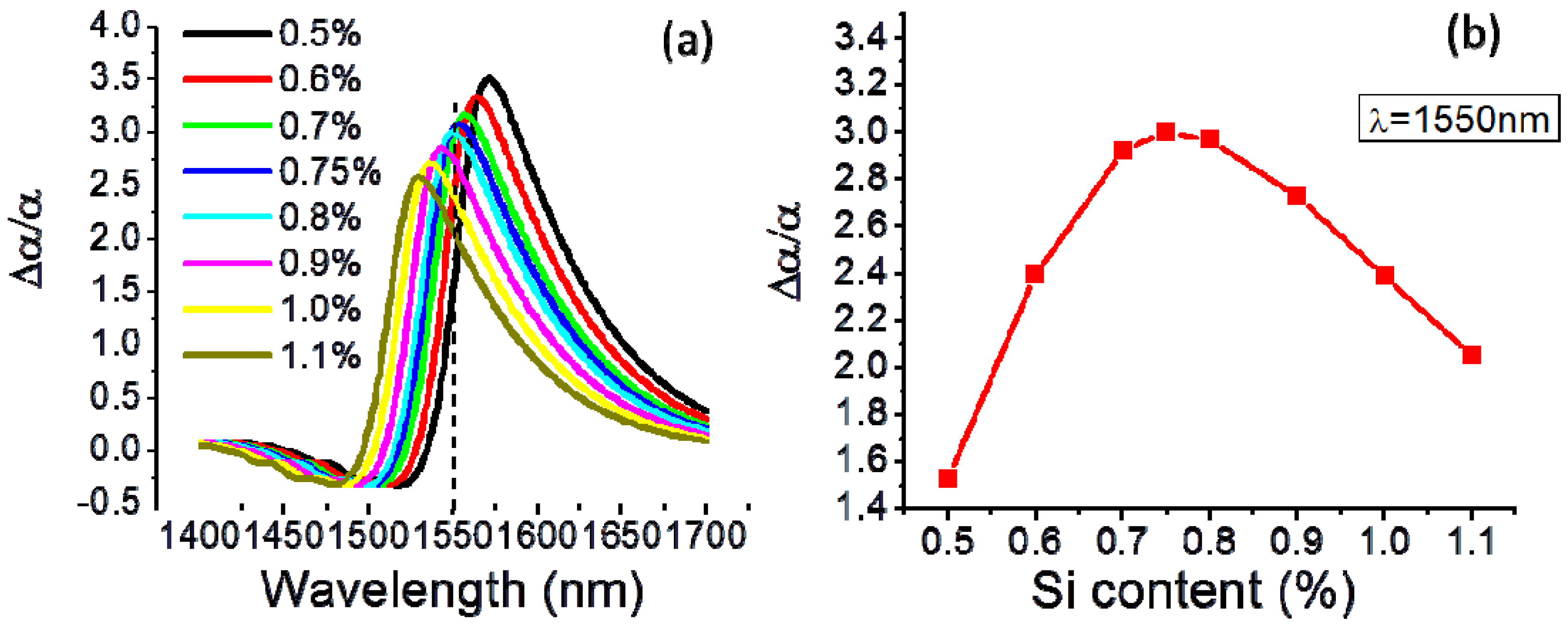
In order to shift the operation wavelength to λ ~ 1550 nm, a small amount of Si can be added to tensile strained Ge to increase the direct band gap of FKE modulators (Figure 12). One should note that the addition of Si tends to decrease Δα/α since it increases the difference between the direct and indirect gaps. Nevertheless, a Δα/α of ~3 can still be achieve at λ ~ 1550 nm [82]. For SiGe/Ge QCSE modulators with a direct band gap corresponding to λ ~ 1430 nm, one could heat up the device to reduce the band gap, apply a larger electric field to extend the EA spectral regime, or utilize some strain engineering approaches (see Section 2.1) to convert the compressive strain into tensile strain. Strain engineering is the most preferred method since it avoids additional power consumption and helps to reduce the energy difference between the direct and indirect gaps in Ge QWs, thereby increasing Δα/α. On the other hand, broad-band QCSE effect has been demonstrated recently by improving the QW design and controlling the DC reverse bias during operation [117]. Different from pervious QW structures, the 0.18% thermally induced tensile strain in the SiGe buffer layer is taken into account to design the QW stack. The Si composition in the buffer layer is increased from 10%–12% to further reduce the lattice mismatch with the Si substrate, and the QW stack is designed to have an average lattice constant identical to the tensile strained Si0.12Ge0.88 buffer layer. The Si composition in the barrier layers is increased from 15%–19% correspondingly. This design enabled thin buffer layers and Ge QW stacks such that the same electric field can be achieved at a lower reverse bias. By measuring the responsivity spectra vs. reverse bias of a vertically incident Ge QW p-i-n photodiode, it was found that the absorption edge can be shifted beyond 1550 nm at −3.3 V reverse bias. A Δα/α of ~3.5 can be achieved at a voltage swing of Vpp = 1 V in S band and C band by increasing the reverse DC offset from −0.4–−3 V. Based on the materials performance, it was predicted that a 200 μm-long waveguide-coupled Ge QW device can achieve 6.5 dB extinction ratio/4 dB insertion loss and 15 dB extinction ratio/7 dB insertion loss at 1550 and 1490 nm, respectively.
Figure 12.
(a) Absorption contrast, Δα/α, as a function of wavelength for GeSi alloys with different Si compositions (b) Δα/α at λ = 1550 nm as a function of Si composition. We assumed an applied electric field of 100 kV/cm and a built-in field of 10 kV/cm at 0 V in the intrinsic GeSi region. Panel (b) is reproduced from [82] with permission from the Optical Society of America under the Author’s Copyright Transfer Agreement.

Table 2 summarizes the performance of Ge EAMs reported in recent years. Compared to Si MZI modulators based on free-carrier induced refractive index changes, GeSi EAMs are based on an ultrafast (<1 ps) and highly efficient field-induced change in absorption near the direct band edge, which enables a very compact device size and an ultralow capacitance. These features are especially advantageous for short-range applications such as photonic links in data centers, while phase-based modulators such as Si MZIs are more favored for coherent transceivers in metro and long-haul applications [118]. Compared to Si microring modulators, GeSi EAMs have a broader range of operation wavelengths and their performance is much less susceptible to temperature variations on chip.
The first waveguide-integrated GeSi EAM was demonstrated using tensile-strain enhanced FKE and a butt-coupling scheme [83]. The material was alloyed with 0.75% Si for operation at 1550 nm wavelength, according to the design in [82]. An extinction ratio of 8 dB at λ = 1550 nm was achieved with an insertion loss of 3.7 dB and a peak-to-peak voltage swing of Vpp = 3 V (from −4 to –−7 V). A 30 GHz waveguide-integrated Ge FKE modulator optimized for L-band operation (1610–1640 nm) [119] and a 40 GHz GeSi (0.7% Si) FKE modulator [120] optimized for 1550 nm operation have been demonstrated by Kotura, Inc. Very recently, a nine-channel GeSi EAM array integrated with 40 nm technology node digital CMOS driver and wavelength multiplexer was reported, marking the entry of waveguide-coupled GeSi EAMs into system level integration. [121] Single channel operation up to 25 Gb/s and nine-channel operation at 10.25 Gb/s has been achieved at a Vpp of 2 V. Evanescently coupled Ge FKE modulators have also been reported [91].
Table 2.
Summary of Ge and GeSi EAM performance. The data are reported for 1550 nm operation, and the voltage swing is from 0 to −Vpp (reverse bias) unless otherwise stated.
| Reference | Optimal Wavelength Range (nm) | Coupling Method | Extinction Ratio (dB) | Insertion Loss (dB) | Bandwidth (GHz) | Vpp (V) | Active Device Area (μm2) | Average Dynamic Energy/bit 1/4 CVpp2 (fJ/bit) |
|---|---|---|---|---|---|---|---|---|
| Ge and GeSi FKE Modulators: | ||||||||
| [83] | 1539–1553 | butt | 8 | 3.7 | 1.2 | 3 (−4 to −7 V) | 0.6 × 50 | 25 a |
| [91] | 1580–1610 | evanescent | 10@ 1600 nm | 9.6 | 1.25 Gb/s | 5 | 0.8 × 20 | 102–103 |
| [119] | 1610–1640 | butt | 6.3@ 1620 nm | 3.6@ 1620 nm | 30 | 4 | 1 × 45 | ~70 |
| [120] | 1545–1581 | butt | 6 | 5 | 40.7 | 2.8 | 1 × 55 | 60 |
| [121] b | 1525–1555 | butt | 3 | 3 | >40; >10 Gb/s for 9 channels | 2 | - | 50 for EAM; 570 including driver |
| Ge QCSE Modulators: | ||||||||
| [122] | 1441–1461 | Side-entry | 7.3@ 1457 nm | ~9@ 1457 nm | - | 10 | 450 × 450 | - |
| [123] | 1415–440 | fiber coupled | 7/10@ 1420 nm | 3/7 dB@ 1420 nm | - | 6 | L = 34/64 μm | - |
| [124] | 1425–1446 | fiber coupled | 9@ 1435 nm Vpp = 1 V | 15@1435 nm, (−3 V) | 23 | 1 (−3 to −4 V) | 3 × 90 | 108 |
| [125] | 1450–1470@ −4 V DC bias c | butt | >3.2@ 1460 | ~15 | 3.5 | 1 (−3 to −5 V) | 0.8 × 10 | 0.75 |
| [126] | 1290–1310 | fiber coupled | 6@ 1293 nm | 2.5 | - | 7 | 3 × 150 | - |
a In [83] a conservative estimate of 50 fJ/bit was reported based on 1/2 CVpp2, considering the most power-consuming scenario of flipping between “on” and “off” states in every operation. b Integrated with 40 nm technology node CMOS driver and wavelength multiplexer. c The operation wavelength range could be redshifted up to 1550 nm at a DC bias of –7.5 V and 1 V voltage swing judging from the photocurrent measurement. The direct modulation data is only available at 1460 nm with −4 V DC bias, though.
The first Ge QCSE modulator was demonstrated using a side-entry approach [122]. The light was coupled through the edge of a lightly doped Si wafer, then incident on a Ge QW mesa grown on top of it. A 7.3 dB extinction ratio at 1457 nm was demonstrated with a Vpp of 10 V. Ge QCSE modulators directly coupled to taper-lensed fibers were investigated in [123]. An extinction ratio greater than 7 dB has been demonstrated at ~1420 nm with ~3 dB insertion loss for a 34 μm-long device. The same group later achieved 23 GHz modulators with 9 dB extinction ratio and Vpp = 1 V (between −3 and −4 V reverse bias) [124]. The insertion loss is partially due to the indirect gap absorption in the thick Si0.1Ge0.9 buffer layer. The first waveguide-integrated Ge QCSE modulator was demonstrated on an SOI substrate using a butt coupling approach. A 3.5 GHz bandwidth was demonstrated at 1460 nm with an extinction ratio >3 dB, using an impressively compact device of 0.8 × 10 μm2 [125]. Although the insertion loss is large due to the optical modal mismatch between the SOI waveguide and the Ge QW active region, it could be improved by optimizing the device design and fabrication. The ultralow capacitance of the device (0.75 fF) and low Vpp = 1 V are highly advantageous for energy-efficient modulation. It is expected that the required DC voltage offset could also be reduced using the improved QW design in [117]. Very recently, a Ge QCSE modulator with Si0.35Ge0.65 barrier layers working at 1300 nm has been reported, covering another important wavelength in optical communications [126].
In summary of this section, the results in Table 2 indicate that Ge and GeSi EAMs are ideal candidates for high bandwidth, high energy-efficiency photonic modulators monolithically integrated on Si.
4.4. Ge Gain Media and Lasers
In 2007, we proposed combing tensile strain with n-type doping to compensate the energy difference between the direct and indirect band gap of Ge, thereby achieving net optical gain for CMOS-compatible LDs [19]. Optical gain [30,127] and lasing at room temperature have been demonstrated experimentally under optical [128] and electrical pumping [129] since then. A recent review on this topic has been presented in [66]. Therefore, in this section we will mainly discuss approaches to further improve the performance of Ge-on-Si LDs based on the most recent results in this field.
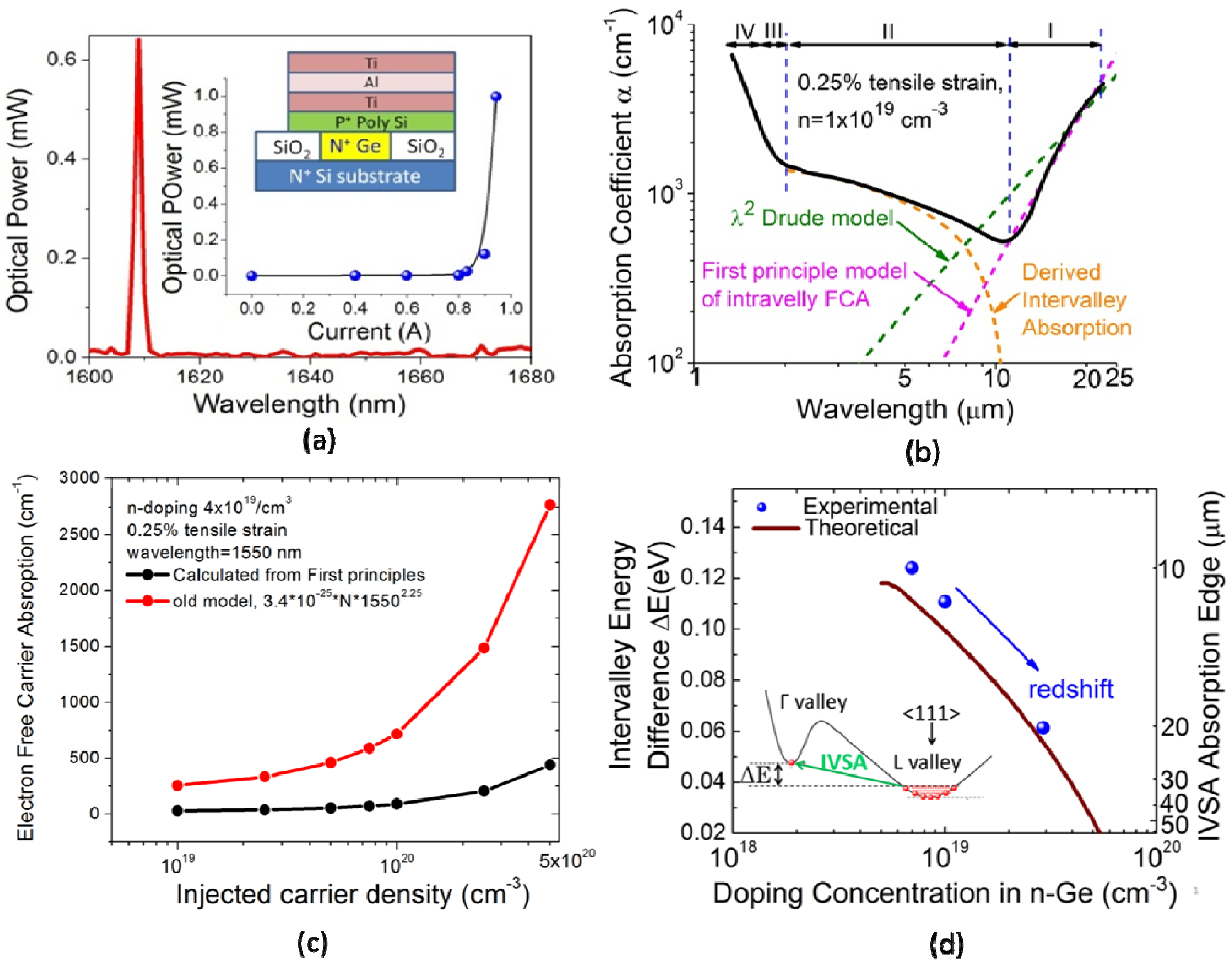
The first electrically-pumped Ge-on-Si LD was based on a simple n+ Si/n+ Ge/p+ Si double heterojunction structure [129]. Compared to optical pumping, the optical gain from the Ge active region has to be increased in order to overcome the FCA losses in the electrodes. As such, the n-type doping level in Ge is increased from 1 × 1019 cm−3 to >4 × 1019 cm−3 using delta-doped capping layers as a dopant reservoir for drive-in diffusion (see Section 2.2 and Section 3.1). Correspondingly, the experimentally measured optical gain increases from 56 cm−1 to >500 cm−1, large enough to overcome the FCA in heavily doped Si and metal electrodes for electrically pumped lasers. Figure 13a shows a representative emission spectrum and L-I curve of an electrically pumped Ge-on-Si laser at room temperature. In this case, the output optical power is ~1 mW at an emission wavelength of 1610 nm. Depending on the thickness of the Ge layer and corresponding modal losses due to FCA in the electrodes, the clamping conditions of lasing vary accordingly and lasing wavelengths in a broad spectrum range of 1530–1660 nm has been observed. Such a broad gain spectrum is consistent with our theoretical predictions [19], and it enables on-chip wavelength division multiplexing (WDM). The observed maximum output power is 8 mW at room temperature. A slope efficiency of ηslope = 2% was demonstrated in an un-optimized device structure. We estimated an internal loss of αi = 636 cm−1 due to FCA (in both n+ Ge region and the Si electrodes) and a mirror loss of αm = 45 cm−1 [55]. Therefore, the internal quantum efficiency (IQE) of this prototype Ge-on-Si diode is estimated to be
The major limiting factor of IQE is likely to be Auger recombination, which tends to be dominated by free holes in Ge. Therefore, reducing the required injected carrier density for transparency is the key to further increasing the efficiency.
In analyzing the experimental data of the prototype Ge-on-Si LD, we noticed that the measured net optical gain is significantly higher than our original theoretical prediction in [19], which assumed the classical Drude model in extrapolating the FCA losses of n+ bulk Ge to λ = 1500–1700 nm. To understand this discrepancy, we measured the absorption spectrum of 0.25% tensile-strained n+ Ge-on-Si using Fourier transform infrared spectroscopy (FTIR). The absorption spectrum of 0.25% tensile strained Ge with n = 1 × 1019 cm−3 is shown in Figure 13b after correction for the wavelength-dependent backside roughness scattering and impurity infrared absorption of the Si substrate [130]. In Regime I, the absorption drastically increases with wavelength at λ > 10 µm, indicating FCA. However, experimentally measured FCA decreases much faster with wavelength than the λ2 Drude model at λ < 15 µm, indicating the breakdown of Drude model in the mid- and near-infrared regime. Instead, the experimental data is in good agreement with first principle calculations of the intra-L-valley (indirect valley) absorption [131] that takes into account the band structure of tensile-strained Ge as well as optical phonon, acoustic phonon and charged impurity scattering mechanisms. Therefore, we recalculated intra-L-valley FCA at λ = 1550 nm using first principle approach and found that the Drude model overestimated the intravalley FCA by an order of magnitude, as shown in Figure 13c [55]. At n = 4 × 1019 cm−3 the FCA coefficient is 20–30 cm−1 in this wavelength range, compared to ~200 cm−1 from the extrapolation of the Drude model. This result agrees with both [131] and Haug’s quantum mechanical analysis [132] showing that intravalley FCA at photon energies larger than the band gap is in the order of 1 cm−1 for mid-1018 cm−3 n-type doping. It indicates that FCA losses are overestimated in our previous theoretical analysis. On the other hand, Figure 13b shows that at λ < 11 μm, the absorption starts to increase again. We proposed that this is due to the onset of intervalley scattering absorption (IVSA) from the indirect L valleys to the direct Γ valley. The observed absorption edges in Regime II for tensile strained Ge samples with different n-type doping levels are consistent with the energy difference between the Γ valley and the Fermi level (Figure 13d, ΔE = EΓ − Ef). The shape of the IVSA absorption curve is also similar to that of the n+ GaAs [133]. Note that the IVSA process in n+ Ge promotes electrons from the indirect L valleys to the direct Г valley, which in turn enhances light emission and optical gain from the direct gap transition of Ge. This process is exactly opposite to the case of III-V semiconductors. The two factors discussed above explain why we observed a higher net gain than the original theoretical modeling.
It is also interesting to note that IVSA has not been observed in previous literature on bulk n+ Ge (0 strain) or slightly compressively strained (−0.07%) n+ Ge grown on GaAs reported recently [134]. Therefore, the 0.25% tensile strain in the n+ Ge films seems to enhance IVSA by decreasing the energy difference between L and Г valleys and making more initial and final states accessible to phonon-assisted IVSA. Indeed, pressure-dependent ab initio calculation shows that the contributions of various phonons to the intervalley scattering are quite dependent on the energy separation between conduction band valleys [135]. Further considering that the inherent optical gain from the direct gap transition of tensile strained n+ Ge is 25× higher than the steady-state gain [136], enhancing L → Γ (indirect-to-direct) intervalley scattering by tensile strain, Sn alloying and/or phonon engineering in nanostructures [137] may help to significantly increase the optical gain of band engineered Ge LDs.
Figure 13.
(a) Schematic cross-section, emission spectrum, and L-I curve of an electrically pumped Ge-on-Si laser at room temperature. The width of the Ge waveguide is 1 μm and the length is 300 μm. (b) Infrared absorption spectrum of 0.25% tensile strained Ge thin film with n = 1 × 1019 cm−3. Regimes I–IV are respectively dominated by intra-L-valley free carrier absorption, L → Г intervalley scattering absorption, indirect gap + intervalley scattering absorption, and direct gap absorption. (c) Comparison of electron free carrier absorption in tensile strained n+ Ge from first-principle model vs. the classical Drude model. © 2013 IEEE. Reprinted, with permission, from [55]. (d) Theoretical and experimental intervalley energy difference between L and Г valleys as a function of doping concentration. The inset schematically illustrates the phenomenon of L → Г intervalley scattering absorption in n+ Ge. Panels (b) and (d) are reproduced from [130] with permission from the Optical Society of America under the Author’s Copyright Transfer Agreement.

Based on the results from the prototype device and the discussions in this paper, there are a number of approaches to further enhance the performance of Ge LDs in future research. (1) Optimize the balance among tensile strain, n-type doping, and Sn alloying. As mentioned in Section 2.4, each of these methods has its own technical difficulties when used alone. However, one could utilize moderate levels of tensile strain, n-type doping and Sn alloying to optimize optical gain and lasing without inducing significant challenges in materials growth and fabrication. Considering the reports of 5.7% uniaxial tensile strain [34], >4 × 1019 cm−3 n-type doping, and 9–10 at % Sn alloying achieved so far, there is a lot of room available for such optimization. For 0.25% tensile strained Ge, our simulations have shown that if the n-type doping is increased to >7 × 1019 cm−3 the threshold current density can be decreased below 1 kA/cm2 at 1600–1700 nm, comparable to III-V double heterojunction lasers [55]. If tensile strain is increased or Sn is incorporated, the n-type doping level can be further decreased and the performance improved. Interestingly, our optical gain simulations show that even for band-engineered Ge right at the indirect-to-direct transition point (EgΓ = EgL), having an n-type doping in the order of mid 1018 cm−3 still enhances the performance of the gain medium. Since the detrimental intra-L-valley FCA of n+ Ge is an order lower than our original estimation, the increase of optical gain far exceeds that of FCA losses when n-type doping is incorporated in this case. Moreover, lower injected carrier density is needed to reach the same level of optical gain. Correspondingly, free hole absorption and hole-hole-electron Auger recombination process—the most dominant loss mechanisms—are also greatly reduced. All these factors can further reduce the threshold current density and increase lasing efficiency. (2) Bufferless selective growth of high quality n+ Ge in narrow trenches ≤1 μm in width. The highly dislocated low-temperature Ge buffer layer has been proved to be an undesirable sink for the dopants in n+ Ge [63] and one of the limiting factors of carrier lifetime [138]. While the buffer layer is necessary for blanket film growth, one can go without it for selective growths in narrow trenches ≤1 μm in width [139,140] without affecting the growth profile or trench filling. This method could improve the material quality at the Ge/Si interface and enhanced the carrier injection efficiency in Ge LDs. (3) Incorporating tensile strain and/or Sn into Ge QWs. As discussed in Section 2.5, the compressive strain in SiGe/Ge QWs as well as the quantum confinement effect itself increases the energy difference between the direct and indirect gaps of Ge QWs. Therefore, under these conditions SiGe/Ge QWs actually perform worse than bulk tensile-strained n+ Ge in optical gain and lasing [55]. With the recent progress in tensile strain engineering, we proposed that tensile strain has to be incorporated into Ge QWs in order to counteract the detrimental effect of epitaxial compressive strain and the adverse quantum confinement effect in SiGe/Ge QWs. Our modeling shows that 0.3% tensile-strained Ge QWs with n > 4.5 × 1019 cm−3 can potentially achieve a threshold of ~500 A/cm2, comparable to the performance of III-V LDs. The further incorporation of Sn alloying offers another handle to optimize the gain and lasing performance from the QW structures. In this case, the energy gap reduction due to tensile strain and Sn alloying can also be partially compensated by the quantum confinement effect. This helps to avoid potential issues related to the leakage current and enhanced Auger recombination in small band gap semiconductors. (4) Separate confinement of Γ vs. L electrons in QW structures. As mentioned in Section 2.5, by adequately designing the band alignment between the barrier and Ge QWs, one can enforce more quantum confinement for the L electrons (deeper well) vs. the Γ electron (shallower well), thereby transforming Ge towards a direct gap semiconductor. This approach overcomes the existing issue of SiGe/Ge quantum wells. One would prefer to use direct gap barrier layers such as AlGaAs to implement such structures effectively. Although using III-V materials for an active region is a significant challenge in CMOS compatible fabrications, using them as barrier layers does not require such high material quality and may allow low-temperature, CMOS compatible fabrications.
Another interesting topic to explore is the optimal relative positions of L vs. Γ valleys for on-chip laser sources without active cooling. As mentioned in Section 2.4, a pseudo-direct gap configuration can enhance the direct gap emission efficiency at high temperature and high injection levels due to enhanced L-to-Γ valley excitation or scattering. Considering that the Auger recombination rate in indirect valleys is orders of magnitude smaller than the direct valleys due to the momentum mismatch, the same reason as its lower radiative recombination efficiency, it may be beneficial to “store” the injected electrons in the L-valley and supply it to the direct Γ valley using the fast intervalley scattering process (sub-ps) [135]. This approach helps to optimize the efficiency as well as the high temperature performance of the band-engineered Ge LDs. Recent progress in Sn alloying and tensile strain will allow us to systematically change the relative energy positions between L and Γ valleys for this investigation. It is also important to study the Auger recombination process in these materials. Spectrally resolved ultrafast pump-probe measurements will likely provide important fundamental information on this aspect, especially distinguishing different processes during the relaxation of the injected carriers.
5. Conclusions
We review the latest progress in monolithic Ge-on-Si active photonic materials and devices, including band engineering, materials growth, device structures, and the current status of Ge PDs, EAMs and LDs. Waveguide-integrated Ge PDs have achieved a performance comparable or even better than their III-V counterparts. High performance of Ge PDs at 0 bias could enable photovoltaic mode receivers with even higher energy efficiency. Ge EAMs have demonstrated ultralow power consumption, high bandwidth, and a reasonably broad operation wavelength range for WDM applications. Both Ge PDs and EAMs have entered system level applications, and they are being commercialized by industry. Based on the results from the first prototype Ge-on-Si LDs and recent investigations on band engineering, FCA and intervalley scattering, we find that it is highly feasible to further improve the performance significantly by optimizing the synergy among tensile strain, Sn alloying, n-type doping, and novel QW structures. Recent progress towards direct growth of single crystal Ge and pseudo-single-crystalline, direct gap GeSn materials on dielectric layers also paves the path towards monolithic 3D photonic integration. Clearly, these high-performance monolithic Ge-on-Si active photonic devices will enable large-scale EPICs on Si.
Acknowledgments
The author’s work on waveguide-integrated GeSi EAMs and Ge PDs had been sponsored under the Defense Advanced Research Projects Agency’s (DARPA) EPIC program supervised by Jagdeep Shah in the Microsystems Technology Office (MTO) under Contract No. HR0011-05-C-0027 from 2003 to 2008. From 2006 to 2011, the authors’ research on Ge lasers was supported by U.S. Air Force Office of Scientific Research’s (AFOSR) Multidisciplinary University Research Initiative (MURI) on Silicon-Based Lasers supervised by Gernot Pomrenke. From 2010–2012, the research on electrically-pumped Ge lasers was also supported by the Fully Laser Integrated Photonics (FLIP) program under APIC Corporation, supervised by Raj Dutt, and sponsored by the Naval Air Warfare Center-Aircraft Division (NAWC-AD) under OTA N00421-03-9-0002. The author’s current work on low-temperature crystallization of pseudo-single-crystalline GeSn on dielectric layers for 3D photonic integration has been sponsored by the National Science Foundation (NSF) under the grant number DMR-1255066.
Conflicts of Interest
The author declares no conflict of interest.
References
- Lannoo, B.; Lambert, S.; van Heddeghem, W.; Pickavet, M.; Kuipers, F.; Koutitas, G.; Niavis, H.; Satsiou, A.; Beck, M.T.; Fischer, A.; et al. Overview of ICT Energy Consumption. Available online: http://www.internet-science.eu/sites/internet-science.eu/files/biblio/EINS_D8%201_final.pdf (accessed on 22 April 2014).
- Klein, T.E. Sustainable ICT Networks: The GreenTouch Vision. Green Research at Alcatel-Lucent. Available online: http://www.greentouch.org/uploads/documents/3%20Thierry%20Klein_EU%20SEW%20-%20The%20GT%20Vision%20-%20v2.pdf (accessed on 22 April 2014).
- Kimerling, L.C. Microphotonics: The Next Platform for the Information Age. 2011 MIT in Japan Conference. Available online: http://ilp.mit.edu/media/conferences/2011-japan/Kimerling.pdf (accessed on 22 April 2014).
- Soref, R.A. The past, present and future of silicon photonics. IEEE J. Sel. Top. Quantum Electron. 2006, 12, 1678–1687. [Google Scholar] [CrossRef]
- Kirchain, R.; Kimerling, L.C. A roadmap for nanophotonics. Nat. Photonics 2007, 1, 303–305. [Google Scholar] [CrossRef]
- Benner, A. Optical interconnect opportunities in supercomputers and high-end computing. In Proceedings of the 2012 Optical Fiber Communication Conference (OFC), Los Angeles, CA, USA, 4–8 March 2012.
- Liu, A.; Jones, R.; Liao, L.; Samara-Rubio, D.; Rubin, D.; Cohen, O.; Nicolaescu, R.; Paniccia, M. A high-speed silicon optical modulator based on metal-oxide-semiconductor capacitor. Nature 2004, 427, 615–618. [Google Scholar] [CrossRef]
- Xu, Q.; Schmidt, B.; Pradhan, S.; Lipson, M. Micrometre-scale silicon electro-optic modulator. Nature 2005, 435, 325–327. [Google Scholar] [CrossRef]
- Timurdogan, E.; Sorace-Agaskar, C.M.; Sun, J.; Hosseini, E.S.; Biberman, A.; Watts, M.R. A One Femtojoule Athermal Silicon Modulator. arXiv:1312.2683. Available online: http://arxiv.org/ftp/arxiv/papers/1312/1312.2683.pdf (accessed on 22 April 2014).
- Lin, H.; Ogbuu, O.; Liu, J.F.; Zhang, L.; Michel, J.; Hu, J.J. Breaking the Energy-Bandwidth Limit of Electrooptic Modulators: Theory and a Device Proposal. J. Light. Technol. 2013, 31, 4029–4036. [Google Scholar]
- Pavesi, L.; dal Negro, L.; Mazzoleni, C.; Franzo, G.; Priolo, F. Optical gain in silicon nanocrystals. Nature 2000, 408, 440–444. [Google Scholar] [CrossRef]
- Wilcoxon, J.P.; Samara, G.A. Tailorable, visible light emission from silicon nanocrystals. Appl. Phys. Lett. 1999, 74, 3164. [Google Scholar] [CrossRef]
- Geis, M.W.; Spector, S.J.; Grein, M.E.; Yoon, J.U.; Lennon, D.M.; Lyszczarz, T.M. Silicon waveguide infrared photodiodes with >35 GHz bandwidth and phototransistors with 50 AW-1 response. Opt. Express 2014, 22, 9150–9158. [Google Scholar]
- Souhan, B.; Grote, R.R.; Driscoll, J.B.; Lu, M.; Stein, A.; Bakhru, H.; Osgood, R.M. Metal-semiconductor-metal ion-implanted Si waveguide photodetectors for C-band operation. Opt. Express 2009, 17, 51–9158. [Google Scholar]
- Cheng, K.Y.; Anthony, R.; Kortshagen, U.R.; Holmes, R.J. High-efficiency silicon nanocrystal light-emitting devices. Nano Lett. 2011, 11, 1952–1956. [Google Scholar] [CrossRef]
- Physics of Group IV Elements and III–V Compounds, Landolt-Börnstein: Numerical Data and Functional Relationships in Science and Technology; Madelung, O. (Ed.) Springer: Berlin, Germany, 1982; Volume 17a.
- Lee, M.J.; Fitzgerald, E.A. Strained Si, SiGe, and Ge channels for high-mobility metal-oxide-semiconductor field-effect transistors. J. Appl. Phys. 2005, 97, 011101. [Google Scholar] [CrossRef]
- Liu, J.F.; Camacho-Aguilera, R.; Sun, X.; Wang, X.X.; Cai, Y.; Kimerling, L.C.; Michel, J. Reprinted from Thin Solid Films, Ge-on-Si Optoelectronics; Elsevier: Amsterdam, The Netherlands, 2011; Volume 520, pp. 3354–3360. [Google Scholar]
- Liu, J.F.; Sun, X.; Pan, D.; Wang, X.X.; Kimerling, L.C.; Koch, T.L.; Michel, J. Tensile-strained, n-type Ge as a gain medium for monolithic laser integration on Si. Opt. Express 2007, 15, 11272–11277. [Google Scholar]
- Soref, R.A.; Friedman, L. 1993b Direct gap Ge/GeSn/Si and GeSn/Ge/Si heterostructures. Superlattice Microstruct. 1993, 14, 189–193. [Google Scholar] [CrossRef]
- El Kurdi, M.; Fishman, G.; Sauvage, S.; Boucaud, P. Band structure and optical gain of tensile-strained germanium based on a 30 band k·p formalism. J. Appl. Phys. 2010, 107, 013710. [Google Scholar] [CrossRef]
- Aldaghri, O.; Ikonic, Z.; Kelsall, R.W. Optimum strain configurations for carrier injection in near infrared Ge lasers. J. Appl. Phys. 2012, 111, 053106. [Google Scholar] [CrossRef]
- Ishikawa, Y.; Wada, K.; Cannon, D.D.; Liu, J.F.; Luan, H.C.; Kimerling, L.C. Strain-induced direct bandgap shrinkage in Ge grown on Si substrate. Appl. Phys. Lett. 2003, 82, 2044–2046. [Google Scholar] [CrossRef]
- Liu, J.F.; Cannon, D.D.; Wada, K.; Ishikawa, Y.; Danielson, D.T.; Jongthammanurak, S.; Michel, J.; Kimerling, L.C. Deformation potential constants of biaxially tensile stressed Ge epitaxial films on Si(100). Phys. Rev. B 2004, 70, 155309. [Google Scholar] [CrossRef]
- Hartmann, J.M.; Abbadie, A.; Papon, A.M.; Holliger, P.; Roland, G.; Billon, T.; Fédéli, J.M.; Rouvière, M.; Vivien, L.; Laval, S. Reduced pressure-chemical vapor deposition of Ge thick layers on Si(001) for 1.3–1.55 µm photodetection. J. Appl. Phys. 2004, 95, 5905–5913. [Google Scholar] [CrossRef]
- Fang, Y.Y.; Tolle, J.; Roucka, R.; Chizmeshiya, A.V.G.; Kouvetakis, J.; D’Costa, V.R.; Menendez, J. Perfectly tetragonal, tensile-strained Ge on Ge1−ySny buffered Si(100). Appl. Phys. Lett. 2007, 90, 061915. [Google Scholar] [CrossRef]
- Takeuchi, S.; Shimura, Y.; Nakatsuka, O.; Zaima, S.; Ogawa, M.; Sakai, A. Growth of highly strain-relaxed Ge1−xSnx/virtual Ge by a Sn precipitation controlled compositionally step-graded method. Appl. Phys. Lett. 2008, 93, 231916. [Google Scholar]
- Liu, J.F.; Cannon, D.D.; Wada, K.; Ishikawa, Y.; Danielson, D.T.; Jongthammanurak, S.; Michel, J.; Kimerling, L.C. Silicidation-induced band gap shrinkage in Ge epitaxial films on Si. Appl. Phys. Lett. 2004, 84, 660–662. [Google Scholar] [CrossRef]
- Kuroyanagi, R.; Ishikawa, Y.; Tsuchizawa, T.; Wada, K. Controlling strain in Ge on Si for EA modulators. In Proceedings of the 8th IEEE International Conference on Group IV Photonics, London, UK, 14–16 September 2011.
- De Kersauson, M.; El Kurdi, M.; David, S.; Checoury, X.; Fishman, G.; Sauvage, S.; Jakomin, R.; Beaudoin, G.; Sagnes, I.; Boucaud, P. Optical gain in single tensile-strained germanium photonic wire. Opt. Express 2011, 19, 17925–17934. [Google Scholar]
- Jain, J.R.; Hryciw, A.; Baer, T.M.; Miller, D.A.B.; Brongersma, M.L.; Howe, R.T. A micromachining-based technology for enhancing germanium light emission via tensile strain. Nat. Photonics 2012, 6, 398–405. [Google Scholar] [CrossRef]
- Süess, M.J.; Geiger, R.; Minamisawa, R.A.; Schiefler, G.; Frigerio, J.; Chrastina, D.; Isella, G.; Spolenak, R.; Faist, J.; Sigg, H. Analysis of enhanced light emission from highly strained germanium microbridges. Nat. Photonics 2013, 7, 466–472. [Google Scholar] [CrossRef]
- Geiger, R.; Süess, M.J.; Bonzon, C.; Spolenak, R.; Faist, J.; Sigg, H. Strained Ge microbridges to obtain a direct bandgap laser. In Proceedings of the 7th International SiGe Technology and Device Meeting, Singapore, Singapore, 2–4 June 2014.
- Sukhdeo, D.S.; Nam, D.; Kang, J.H.; Brongersma, M.L.; Saraswat, K.C. Direct bandgap germanium-on-silicon inferred from 5.7% <100> uniaxial tensile strain. Photonics Res. 2014, 2, A8–A13. [Google Scholar] [CrossRef]
- Capellini, G.; Reich, C.; Guha, S.; Yamamoto, Y.; Lisker, M.; Virgilio, M.; Ghrib, A.; el Kurdi, M.; Boucaud, P.; Tillack, B.; et al. Tensile Ge microstructures for lasing fabricatedby means of a silicon complementary metal oxide-semiconductor process. Opt. Express 2014, 22, 399–410. [Google Scholar] [CrossRef]
- Haynes, J.R.; Nilsson, N.G. The direct radiative transitions in germanium and their use in the analysis of lifetime. In Proceedings of the VIIth International Conference on Physics of Semiconductors, Paris, France; 1964; pp. 21–31. [Google Scholar]
- Spitzer, W.G.; Trumbore, F.A.; Logan, R.A. Properties of heavily doped n-type germanium. J. Appl. Phys. 1961, 32, 1822–1830. [Google Scholar] [CrossRef]
- Newman, R.; Tyler, W.W. Effect of impurities on free-hole infrared absorption in p-type germanium. Phys. Rev. 1957, 105, 885–886. [Google Scholar] [CrossRef]
- Carroll, L.; Friedli, P.; Neuenschwander, S.; Sigg, H.; Cecchi, S.; Isa, F.; Chrastina, D.; Isella, G; Fedoryshyn, Y.; Faist, J. Direct-gap gain and optical absorption in germanium correlated to the density of photoexcited carriers doping, and strain. Phys. Rev. Lett. 2012, 109, 057402. [Google Scholar]
- Jenkins, J.W.; Dow, J.D. Electronic properties of metastable Ge1−xSnx alloys. Phys. Rev. B 1987, 36, 7994–8000. [Google Scholar] [CrossRef]
- He, G.; Atwater, H.A. Interband transitions in SnxGe1−x alloys. Phys. Rev. Lett. 1997, 79, 1937–1940. [Google Scholar] [CrossRef]
- Soref, R.; Kouvetakis, J.; Tolle, J.; Menendez, J.; D’Costa, V. Advances in SiGeSn technology. J. Mater. Res. 2007, 22, 3281–3291. [Google Scholar] [CrossRef]
- Mathews, J.; Roucka, R.; Xie, J.Q.; Yu, S.Q.; Menéndez, J.; and Kouvetakis, J. Extended performance GeSn/Si(100) p-i-n photodetectors for full spectral range telecommunication applications. Appl. Phys. Lett. 2009, 95, 133506. [Google Scholar]
- D’Costa, V.R.; Cook, C.S.; Birdwell, A.G.; Littler, C.L.; Canonico, M.; Zollner, S.; Kouvetakis, J.; Menéndez, J. Optical critical points of thin-film Ge1−ySny alloys: A comparative Ge1−ySny/Ge1−xSix study. Phys. Rev. B 2006, 73, 125207. [Google Scholar] [CrossRef]
- Chen, R.; Lin, H.; Huo, Y.; Hitzman, C.; Kamins, T.I.; Harris, J.S. Increased photoluminescence of strain-reduced, high-Sn composition Ge1−xSnx alloys grown by molecular beam epitaxy. Appl. Phys. Lett. 2011, 99, 181125. [Google Scholar]
- Oehme, M.; Buca, D.; Kostecki, K.; Wirths, S.; Hollaender, B.; Kasper, E.; Schulze, J. Epitaxial growth of highly compressively strained GeSn alloys up to 12.5% Sn. J. Cryst. Growth 2013, 384, 71–76. [Google Scholar] [CrossRef]
- Li, H.; Brouillet, J.; Salas, A.; Wang, X.X.; Liu, J.F. Low Temperature Growth of High Crystallinity GeSn on Amorphous Layers for Advanced Optoelectronics. Opt. Mater. Express 2013, 3, 1385–1396. [Google Scholar] [CrossRef]
- Oehme, M.; Kostecki, K.; Schmid, M.; Oliveira, F.; Kasper, E.; Schulze, J. Epitaxial growth of strained and unstrained GeSn alloys up to 25% Sn. Thin Solid Films 2014, 557, 169–172. [Google Scholar] [CrossRef]
- Van de Walle, C.G. Band lineups and deformation potentials in model-solid theory. Phys. Rev. B 1989, 39, 1871–1883. [Google Scholar] [CrossRef]
- Sun, X.; Liu, J.F.; Kimerling, L.C.; Michel, J. Direct gap photoluminescence of n-type tensile-strained Ge-on-Si. Appl. Phys. Lett. 2009, 95, 011911. [Google Scholar] [CrossRef]
- Bessette, J.; Camacho-Aguilera, R.; Cai, Y.; Kimerling, L.C.; Michel, J. Optical characterization of Ge-on-Si laser gain media. In Proceedings of the 8th IEEE International Conference on Group IV Photonics, London, UK, 14–16 September 2011. paper # P1.25.
- Sun, X.; Liu, J.F.; Kimerling, L.C.; Michel, J. Room-temperature direct bandgap electroluminesence from Ge-on-Si light-emitting diodes. Opt. Lett. 2009, 34, 1198–1200. [Google Scholar] [CrossRef]
- Cheng, S.L.; Lu, J.; Shambat, G.; Yu, H.Y.; Saraswat, K.; Vuckovic, J.; Nishi, Y. Room Temperature 1.6 μm electroluminescence from Ge light emitting Diode on Si Substrate. Opt. Express 2009, 17, 10019–10024. [Google Scholar]
- Arguirov, T.; Kittler, M.; Oehme, M.; Abrosimov, N.V.; Kasper, E.; Schulze, J. Room temperature direct band-gap emission from an unstrained Ge p-i-n LED on Si. Solid. State. Phenom. 2011, 178–179, 25–30. [Google Scholar] [CrossRef]
- Cai, Y.; Han, Z.; Wang, X.X.; Camacho-Aguilera, R.E.; Kimerling, L.C.; Michel, J.; Liu, J.F. Analysis of threshold current behavior for bulk and quantum well germanium laser structures. IEEE J. Sel. Top. Quantum Electron. 2013, 19, 1901009. [Google Scholar] [CrossRef]
- Froyen, S.; Wood, D.M.; Zunger, A. Electronic-structure of ultrathin SinGen strained superlattices—The possibility of direct band-gaps. Thin Solid Films 1989, 183, 33–48. [Google Scholar] [CrossRef]
- Kholod, A.N.; Ossicini, S.; Borisenko, V.E.; Arnaud d’Avitaya, F. True direct gap absorption in germanium quantum films. Phys. Rev. B. 2002, 65, 115315. [Google Scholar] [CrossRef]
- Virgilio, M.; Grosso, G. Type-I alignment and direct fundamental gap in SiGe based hetero-structures. J. Phys. C. Condens. Matter 2006, 18, 1021–1031. [Google Scholar] [CrossRef]
- Baribeau, J.M.; Jackman, T.E.; Houghton, D.C.; Maigné, P.; Denhoff, M.W. Growth and Characterization of Si1−xGex and Ge Epilayers on (100) Si. J. Appl. Phys. 1988, 63, 5738–5746. [Google Scholar] [CrossRef]
- Colace, L.; Masini, G.; Galluzzi, F.; Assanto, G.; Capellini, G.; di Gaspare, L.; Evangelisti, F. Ge/Si (001) photodetector for infrared light. Solid State Phenom. 1997, 54, 55–58. [Google Scholar] [CrossRef]
- Luan, H.C.; Lim, D.R.; Lee, K.K.; Chen, K.M.; Sandland, J.G.; Wada, K.; Kimerling, L.C. High-quality Ge epilayers on Si with low threading-dislocation densities. Appl. Phys. Lett. 1999, 75, 2909–2911. [Google Scholar] [CrossRef]
- Luan, H.-C. Ge Photodetectors for Si Microphotonics. Ph.D. Thesis, Massachusetts Institute of Technology, Cambridge, MA, USA, 2001; pp. 74–76, 98–100. [Google Scholar]
- Tachikawa, M.; Yamaguchi, M. Film thickness dependence of dislocation reduction in GaAs-on-Si substrates. Appl. Phys. Lett. 1990, 54, 584–486. [Google Scholar]
- Romanova, A.E.; Pompe, W.; Beltz, G.E.; Speck, J.S. An approach to threading dislocation “reaction kinetics”. Appl. Phys. Lett. 1996, 69, 3342–3344. [Google Scholar] [CrossRef]
- Yamamoto, Y.; Kozlowski, G.; Zaumseil, P.; Tillack, B. Low threading dislocation Ge on Si by combining deposition and etching. Thin Solid Films 2012, 520, 3216–3221. [Google Scholar] [CrossRef]
- Liu, J.F.; Kimerling, L.C.; Michel, J. Monolithic Ge-on-Si lasers for large-scale electronic-photonic integration. Semicond. Sci. Technol. 2012, 27, 094006. [Google Scholar] [CrossRef]
- Liu, J.F.; Camacho-Aguilera, R.; Sun, X.; Wang, X.X.; Cai, Y.; Kimerling, L.C.; Michel, J. Ge-on-Si Optoelectronics. Thin Solid Films 2012, 520, 3354–3360. [Google Scholar] [CrossRef]
- Michel, J.; Liu, J.F.; Kimerling, L.C. High-Performance Ge-on-Si Photodetectors. Nat. Photonics 2010, 4, 527–534. [Google Scholar] [CrossRef]
- Camacho-Aguilera, R.E.; Cai, Y.; Bessette, J.T.; Kimerling, L.C.; Michel, J. High active carrier concentration in n-type, thin film Ge using delta-doping. Opt. Mater. Express 2012, 2, 1462–1469. [Google Scholar] [CrossRef]
- Cai, Y.; Camacho-Aguilera, R.E.; Bessette, J.T.; Kimerling, L.C.; Michel, J. High phosphorous doped germanium: Dopant diffusion and modeling. J. Appl. Phys. 2012, 112, 034509. [Google Scholar]
- Bauer, M.; Taraci, J.; Tolle, J.; Chizmeshya, A.V.G.; Zollner, S.; Smith, D. J.; Menendez, J.; Hu, C.W.; Kouvetakis, J. Ge-Sn semiconductors for band-gap and lattice engineering. Appl. Phys. Lett. 2002, 81, 2992–2994. [Google Scholar] [CrossRef]
- Mathews, J.; Beeler, R.T.; Tolle, J.; Xu, C.; Roucka, R.; Kouvetakis, J.; Menendez, J. Direct-gap photoluminescence with tunable emission wavelength in Ge1−ySny alloys on silicon. Appl. Phys. Lett. 2010, 97, 221912. [Google Scholar] [CrossRef]
- Liu, Y.; Deal, M.D.; Plummer, J.D. High-quality single-crystal Ge on insulator by liquid-phase epitaxy on Si substrate. Appl. Phys. Lett. 2004, 84, 2563–2565. [Google Scholar] [CrossRef]
- Miyao, M.; Toko, K.; Tanaka, T.; Sadohm, T. High-quality single-crystal Ge stripes on quartz substrate by rapid-melting-growth. Appl. Phys. Lett. 2009, 95, 022115. [Google Scholar] [CrossRef]
- Assefa, S.; Xia, F.N.; Bedell, S.W.; Zhang, Y.; Topuria, T.; Rice, P.M.; Vlasov, Y.A. CMOS-integrated high-speed MSM germanium waveguide photodetector. Opt. Express 2010, 18, 4986–4999. [Google Scholar]
- Matsue, M.; Yasutake, Y.; Fukatsu, S.; Hosoi, T.; Shimura, T.; Watanabe, H. Strain-induced direct band gap shrinkage in local Ge-on-insulator structures fabricated by lateral liquid-phase epitaxy. Appl. Phys. Lett. 2014, 104, 031106. [Google Scholar]
- Kanno, H.; Atsushi, K.; Sadoh, T.; Miyao, M. Ge-enhanced MILC velocity in a-Ge/a-Si/SiO2 layered structure. Mater. Sci. Semicond. Process. 2005, 8, 83–88. [Google Scholar] [CrossRef]
- Yu, C.H.; Yeh, P.H.; Cheng, S.L.; Chen, L.J.; Cheng, L.W. Metal-induced crystallization of amorphous Si1−xGex by rapid thermal annealing. Thin Solid Films 2004, 469–470, 356–360. [Google Scholar] [CrossRef]
- Yang, C.M.; Atwater, H.A. Selective solid phase crystallization for control of grain size and location in Ge thin films on silicon dioxide. Appl. Phys. Lett. 1996, 68, 3392–3394. [Google Scholar] [CrossRef]
- Schropp, R.E.I.; Carius, R.; Beaucarne, G. Amorphous silicon, microcrystalline silicon, and thin- film polycrystalline silicon solar cells. MRS Bull. 2007, 32, 219–224. [Google Scholar] [CrossRef]
- McComber, K.; Duan, X.; Liu, J.F.; Michel, J.; Kimerling, L.C. Single-crystal germanium growth on amorphous silicon. Adv. Funct. Mater. 2012, 22, 1048–1057. [Google Scholar] [CrossRef]
- Liu, J.F.; Dong, P.; Jongthammanurak, S.; Wada, K.; Kimerling, L.C.; and Michel, J. Design of monolithically integrated GeSi electroabsorption modulators and photodetectors on an SOI platform. Opt. Express 2007, 15, 623–628. [Google Scholar] [CrossRef]
- Liu, J.F.; Beals, M.; Pomerene, A.; Bernardis, S.; Sun, R.; Cheng, J.; Kimerling, L.C.; Michel, J. Waveguide integrated, ultra-low energy GeSi electro-absorption modulators. Nat. Photonics 2008, 2, 433–437. [Google Scholar] [CrossRef]
- Beals, M.; Michel, J.; Liu, J.F.; Ahn, D.H.; Sparacin, D.; Sun, R.; Hong, C.Y.; Kimerling, L.C.; Pomerene, A.; Carothers, D.; et al. Process flow innovations for photonic device integration in CMOS. Proc. Int. Soc. Opt. Eng. 2008, 6898, 689804. [Google Scholar]
- Vivien, L.; Osmond, J.; Fédéli, J.M.; Delphine, M.M.; Crozat, P.; Damlencourt, J.F.; Cassan, E.; Lecunff, Y.; Laval, S. 42 GHz p.i.n Germanium photodetector integrated in a silicon-on-insulator waveguide. Opt. Express 2009, 17, 6252–6257. [Google Scholar] [CrossRef]
- Feng, D.; Liao, S.; Dong, P.; Feng, N.N.; Liang, H.; Zheng, D.W.; Kung, C.C.; Fong, J.; Shafiiha, R.; Cunningham, J.; et al. High-speed Ge photodetector monolithically integrated with large cross-section silicon-on-insulator waveguide. Appl. Phys. Lett. 2009, 95, 261105. [Google Scholar] [CrossRef]
- Ren, S.; Kamins, T.I.; Miller, D.A.B. Thin dielectric spacer for the monolithic integration of bulk germanium or germanium quantum wells with silicon-on-insulator waveguides. IEEE. Photonics J. 2011, 3, 739–747. [Google Scholar] [CrossRef]
- Liu, J.F.; Pan, D.; Jongthammanurak, S.; Ahn, D.; Hong, C.Y.; Beals, M.; Kimerling, L.C.; Michel, J.; Pomerene, A.T.; Hill, C.; et al. Waveguide-Integrated Ge p-i-n Photodetectors on SOI Platform. In Proceedings of the 2006 IEEE International Conference on Group IV Photonics, Ottawa, ON, Canada, 13–15 September 2006. paper # ThA2.
- Ahn, D.; Kimerling, L.C.; Michel, J. Evanescent coupling device design for waveguide-integrated group IV photodetectors. J. Light. Technol. 2010, 28, 3387–3394. [Google Scholar]
- Ahn, D.H.; Kimerling, L.C.; Michel, J. Efficient evanescent wave coupling conditions for waveguide-integrated thin-film Si/Ge photodetectors on silicon-on-insulator/germanium-on-insulator substrates. J. Appl. Phys. 2011, 110, 083115. [Google Scholar] [CrossRef]
- Lim, A.E.-J.; Liow, T.Y.; Qing, F.; Duan, N.; Ding, L.; Yu, M.; Lo, G.-Q.; Kwong, D.L. Novel evanescent-coupled germanium electro-absorption modulator featuring monolithic integration with germanium p-i-n photodetector. Opt. Express 2011, 19, 5040–5046. [Google Scholar]
- Wang, X.X.; Liu, J.F. Step-coupler for efficient waveguide coupling to Ge/Si avalanche photodetectors. IEEE. Photonics Technol. Lett. 2011, 23, 146–148. [Google Scholar] [CrossRef]
- Liu, J.F.; Michel, J.; Giziewicz, W.; Pan, D.; Wada, K.; Cannon, D.D.; Kimerling, L.C.; Chen, J.; Ilday, F.O.; Kaertner, F.X.; et al. High-performance, tensile-strained Ge p-i-n photodetectors on a Si platform. Appl. Phys. Lett. 2005, 87, 103501. [Google Scholar] [CrossRef]
- Jutzi, M.; Berroth, M.; Wohl, G.; Oehme, M.; Kasper, E. Ge-on-Si vertical incidence photodiodes with 39-G Hz bandwidth. IEEE Photonics Technol. Lett. 2005, 17, 1510–1512. [Google Scholar] [CrossRef]
- Morse, M.; Dosunmu, O.; Sarid, G.; Chetrit, Y. IEEE. Photonics Technol. Lett. 2006, 18, 2442–2444. [CrossRef]
- Klinger, S.; Berroth, M.; Kaschel, M.; Oehme, M.; Kasper, E. Ge-on-Si p-i-n photodiodes with a 3-dB bandwidth of 49 GHz. IEEE Photonics Technol. Lett. 2009, 21, 920–922. [Google Scholar] [CrossRef]
- DiLello, N.A.; Johnstone, D.K.; Hoyt, J.L. Characterization of dark current in Ge-on-Si photodiodes. J. Appl. Phys. 2012, 112, 054506. [Google Scholar] [CrossRef]
- Colace, L.; Ferrara, P.; Assanto, G.; Fulgoni, D.; Nash, L. Low dark-current germanium-on silicon near-infrared detectors. IEEE. Photonics Technol. Lett. 2007, 19, 1813–1815. [Google Scholar] [CrossRef]
- Oehme, M.; Kostecki, K.; Ye, K.; Bechler, S.; Ulbricht, K.; Schmid, M.; Kaschel, M.; Gollhofer, M.; Körner, R.; Zhang, W.; et al. GeSn-on-Si normal incidence photodetectors with bandwidths more than 40 GHz. Opt. Express 2014, 22, 839–846. [Google Scholar] [CrossRef]
- Deliwala, S. Integrated optical receivers. In Proceedings of the 2011 IEEE International Conference on Group IV Photonics, London, UK, 14 September 2011.
- Kim, I.G.; Jang, K.S.; Joo, J.; Kim, S.; Kim, S.; Choi, K.S.; Oh, J.H.; Kim, S.A.; Kim, G. High-performance photoreceivers based on vertical-illumination type Ge-on-Si photodetectors operating up to 43 Gb/s at λ ~ 1550 nm. Opt. Express 2013, 21, 30718. [Google Scholar]
- Kang, Y.; Liu, H.D.; Morse, M.; Paniccia, M.J.; Zadka, M.; Litski, S.; Sarid, G.; Pauchard, A.; Kuo, Y.H.; Chen, H.W.; et al. Monolithic germanium/silicon avalanche photodiodes with 340 GHz gain-bandwidth product. Nat. Photonics 2009, 3, 59–63. [Google Scholar] [CrossRef]
- Huang, M.; Cai, P.; Wang, L.; Shi, T.; Chen, W.; Li, S.; Hou, G.; Hong, C.-Y.; Dong, P. Development of Si photonics technology: Ge/Si avalanche photodiode for PON applications. In Proceedings of the 2014 Optical Fiber Communication Conference (OFC 2014), San Francisco, CA, USA, 9–13 March 2014. paper # Tu2C2.
- Ahn, D.; Hong, C.Y.; Liu, J.F.; Giziewicz, W.; Beals, M.; Kimerling, L.C.; Michel, J. High performance, waveguide integrated Ge photodetectors. Opt. Express 2007, 15, 3916–3921. [Google Scholar]
- Vivien, L.; Rouvière, M.; Fédéli, J.M.; Marris-Morini, D.E.; Damlencourt, J.F.; Mangeney, J.; Crozat, P.; el Melhaoui, L.; Cassan, E.; le Roux, X.; et al. High speed and high responsivity germanium photodetector integrated in a silicon-on-insulator microwaveguide. Opt. Express 2007, 15, 9843–9848. [Google Scholar] [CrossRef]
- Chen, L.; Preston, K.; Manipatruni, S.; Lipson, M. Integrated GHz silicon photonic interconnect with micrometer-scale modulators and detectors. Opt. Express 2009, 18, 15248–15256. [Google Scholar]
- Novack, A.; Gould, M.; Yang, Y.; Xuan, Z.; Streshinsky, M.; Liu, Y.; Capellini, G.; Lim, A.E.J.; Lo, G.Q.; Baehr-Jones, T.; et al. Germanium photodetector with 60 GHz bandwidth using inductive gain peaking. Opt. Express 2013, 21, 28387–28393. [Google Scholar]
- Vivien, L.; Polzer, A.; Marris-Morini, D.; Osmond, J.; Hartmann, J.M.; Crozat, P.; Cassan, E.; Kopp, C.; Zimmermann, H.; Fédéli, J.M. Zero-bias 40 Gbit/s germanium waveguide photodetector on silicon. Opt. Express 2012, 20, 1096–1101. [Google Scholar] [CrossRef]
- Feng, D.D.; Qian, W.; Liang, H.; Luff, B.J.; Asghari, M. High-speed receiver technology on the SOI platform. IEEE. J. Sel. Top. Quantum Electron. 2013, 19, 3800108. [Google Scholar] [CrossRef]
- Kang, Y.M.; Morse, M.; Paniccia, M.J.; Zadka, M.; Saad, Y.; Sarid, G.; Pauchard, A.; Zaoui, W.S.; Chen, H.W.; Dai, D.; et al. Monolithic Ge/Si avalanche photodiodes. In Proceedings of the 2009 IEEE International Conference on Group IV Photonic, San Francisco, CA, USA, 9–11 September 2009; pp. 25–27.
- Assefa, S.; Xia, F.; Vlasov, Y.A. Reinventing germanium avalanche photodetector for nanophotonic on-chip optical interconnects. Nature 2010, 464, 80–85. [Google Scholar] [CrossRef]
- Liao, S.; Feng, N.-N.; Feng, D.; Dong, P.; Shafiiha, R.; Kung, C.-C.; Liang, H.; Qian, W.; Liu, Y.; Fong, J.; et al. 36 GHz submicron silicon waveguide germanium photodetector. Opt. Express 2011, 19, 10967–10972. [Google Scholar] [CrossRef]
- Pollak, F.H. Study of semiconductor surfaces and interfaces using electromodulation. Surf. Interface Anal. 2001, 31, 938–953. [Google Scholar] [CrossRef]
- Chuang, S.L. Physics of Optoelectronic Devices; Wiley: New York, NY, USA, 1995; Chapter 13. [Google Scholar]
- Jongthammanurak, S.; Liu, J.F.; Wada, K.; Cannon, D.D.; Danielson, D.T.; Pan, D.; Kimerling, L.C.; Michel, J. Large Electro-optic Effect in Tensile Strained Ge-on-Si Films. Appl. Phys. Lett. 2006, 89, 161115. [Google Scholar] [CrossRef]
- Kuo, Y.H.; Lee, Y.K.; Ge, Y.; Ren, S.; Roth, J.E.; Kamins, T.I.; Miller, D.A.B.; Harris, J.S. Strong quantum-confined Stark effect in germanium quantum-well structures on silicon. Nature 2005, 437, 1334–1336. [Google Scholar] [CrossRef]
- Edwards, E.H.; Lever, L.; Fei, E.T.; Kamins, T.I.; Ikonic, Z.; Harris, J.S.; Kelsall, R.W.; Miller, D.A.B. Low-voltage broad-band electroabsorption from thin Ge/SiGe quantum wells epitaxially grown on silicon. Opt. Express 2013, 21, 867–876. [Google Scholar] [CrossRef]
- Doerr, C.R.; Chen, L.Z.; Vermeulen, D.; Nielsen, T.; Azemati, S.; Stulz, S.; McBrien, G.; Xu, X.; Mikkelsen, B.; Givehchi, M.; et al. Single-chip silicon photonics 100-Gb/s coherent transceiver. In Proceedings of the 2014 Optical Fiber Communication Conference, San Francisco, CA, USA, 9–13 March 2014.
- Feng, N.N.; Feng, D.Z.; Liao, S.; Wang, X.; Dong, P.; Liang, H.; Kung, C.C.; Qian, W.; Fong, J.; Shafiiha, R.; et al. 30 GHz Ge electro-absorption modulator integrated with 3 μm silicon-on-insulator waveguide. Opt. Express 2011, 19, 7062–7067. [Google Scholar] [CrossRef]
- Feng, D.Z.; Liao, S.; Liang, H.; Fong, J.; Bijlani, B.; Shafiiha, R.; Luff, B.J.; Luo, Y.; Cunningham, J.E.; Krishnamoorthy, A.V.; et al. High speed GeSi electro-absorption modulator at 1550 nm wavelength on SOI waveguide. Opt. Express 2012, 20, 22224–22232. [Google Scholar] [CrossRef]
- Krishnamoorthy, A.V.; Zheng, X.; Feng, D.; Lexau, J.; Buckwalter, J.F.; Thacker, H.D.; Liu, F.; Luo, Y.; Chang, E.; Amberg, P.; et al. A low-power, high-speed, 9-channel germaniumsilicon electro-absorption modulator array integrated with digital CMOS driver and wavelength multiplexer. Opt. Express 2014, 22, 12289–12295. [Google Scholar] [CrossRef]
- Roth, J.E.; Fidaner, O.; Schaevitz, R.K.; Kuo, Y.H.; Kamins, T.I.; Harris, J.S.; Miller, D.A.B. Optical modulator on silicon employing germanium quantum wells. Opt. Express 2007, 15, 5851–5859. [Google Scholar]
- Chaisakul, P.; Marris-Morini, D.; Isella, G.; Chrastina, D.; le Roux, X.; Edmond, S.; Coudevylle, J.R.; Cassan, E.; Vivien, L. Polarization dependence of quantum-confined Stark effect in Ge/SiGe quantum well planar waveguides. Opt. Lett. 2011, 36, 1794–1796. [Google Scholar] [CrossRef]
- Chaisakul, P.; Marris-Morini, D.; Rouifed, M.-S.; Isella, G.; Chrastina, D.; Frigerio, J.; le Roux, X.; Edmond, S.; Coudevylle, J.-R.; Vivien, L. 23 GHz Ge/SiGe multiple quantum well electro-absorption modulator. Opt. Express 2012, 20, 3219–3224. [Google Scholar] [CrossRef]
- Ren, S.; Rong, Y.; Claussen, S.A.; Schaevitz, R.K.; Kamins, T.I.; Harris, J.S.; Miller, D.A.B. Ge/SiGe quantum well waveguide modulator monolithically integrated with SOI waveguides. IEEE Photonics Technol. Lett. 2012, 24, 461–463. [Google Scholar] [CrossRef]
- Rouifed, M.S.; Marris-Morini, D.; Chaisakul, P.; Frigerio, J.; Isella, G.; Chrastina, D.; Edmond, S.; Roux, X.L.; Coudevylle, J.R.; Bouville, D.; et al. Advances toward Ge/SiGe quantum-well waveguide modulators at 1.3 μm. IEEE. J. Sel. Top. Quantum Electron. 2014, 20, 3400207. [Google Scholar]
- Liu, J.F.; Sun, X.C.; Kimerling, L.C.; Michel, J. Direct-gap optical gain of Ge on Si at room temperature. Opt. Lett. 2009, 34, 1738–1740. [Google Scholar] [CrossRef]
- Liu, J.F.; Sun, X.; Camacho-Aguilera, R.; Kimerling, L.C.; Michel, J. Ge-on-Si laser operating at room temperature. Opt. Lett. 2010, 35, 679–681. [Google Scholar] [CrossRef]
- Camacho-Aguilera, R.E.; Cai, Y.; Patel, N.; Bessette, J.T.; Romagnoli, M.; Kimerling, L.C.; Michel, J. An electrically pumped germanium laser. Opt. Express 2012, 20, 11316–11320. [Google Scholar] [CrossRef]
- Wang, X.X.; Li, H.; Camacho-Aguilera, R.E.; Cai, Y.; Kimerling, L.C.; Michel, J.; Liu, J.F. Infrared absorption of n-type tensile-strained Ge-on-Si. Opt. Lett. 2013, 38, 652–654. [Google Scholar] [CrossRef]
- Tsai, C.-Y.; Tsai, C.-Y.; Chen, C.-H.; Sung, T.L.; Wu, T.-Y.; Shih, F.-P. Theoretical model for intravalley and intervalley free-Carrier absorption in semiconductor lasers: Beyond the classical Drude model. IEEE J. Quantun Electron. 1998, 34, 552–559. [Google Scholar] [CrossRef]
- Haug, A. Free carrier absorption in semiconductor lasers. Semicond. Sci. Technol. 1992, 7, 373–378. [Google Scholar] [CrossRef]
- Spitzer, W.G.; Whelan, J.M. Infrared absorption and electron effective mass in n-type gallium arsenide. Phys. Rev. 1959, 114, 59–63. [Google Scholar] [CrossRef]
- Boucaud, P.; el Kurdi, M.; Ghrib, A.; Prost, M.; de Kersauson, M.; Sauvage, S.; Aniel, F.; Checoury, X.; Beaudoin, G.; Largeau, L.; et al. Recent advances in germanium emission. Photonics Res. 2013, 1, 102–109. [Google Scholar]
- Tyulerev, V.G.; Obukhov, S.V.; Vast, M.; Sjakste, J. Ab initio calculation of electron-phonon scattering time in germanium. Phys. Rev. B 2011, 84, 035201. [Google Scholar]
- Wang, X.X.; Kimerling, L.C.; Michel, J.; Liu, J.F. Large inherent optical gain from the direct gap transition of Ge thin films. Appl. Phys. Lett. 2013, 102, 131116. [Google Scholar] [CrossRef]
- Stroscio, M.A.; Dutta, M. Phonons in Nanostructures; Cambridge University Press: Cambridge, UK, 2004. [Google Scholar]
- Geiger, R.; Frigerio, J.; Süess, M.J.; Chrastina, D.; Isella, G.; Spolenak, R.; Faist, J.; Sigg, H. Excess carrier lifetimes in Ge layers on Si. Appl. Phys. Lett. 2014, 104, 062106. [Google Scholar]
- Langdo, T. Selective SiGe Nanostructures. Ph.D. Thesis, Massachusetts Institute of Technology, Cambridge, MA, USA, 2001. [Google Scholar]
- Camacho-Aguilera, R.E.; Cai, Y.; Kimerling, L.C.; Michel, J. Ge-on-Si bufferless epitaxial growth for photonic devices. ECS Trans. 2012, 50, 469–473. [Google Scholar] [CrossRef]
© 2014 by the authors; licensee MDPI, Basel, Switzerland. This article is an open access article distributed under the terms and conditions of the Creative Commons Attribution license (http://creativecommons.org/licenses/by/3.0/).
Share and Cite
MDPI and ACS Style
Liu, J. Monolithically Integrated Ge-on-Si Active Photonics. Photonics 2014, 1, 162-197. https://doi.org/10.3390/photonics1030162
AMA Style
Liu J. Monolithically Integrated Ge-on-Si Active Photonics. Photonics. 2014; 1(3):162-197. https://doi.org/10.3390/photonics1030162
Chicago/Turabian StyleLiu, Jifeng. 2014. "Monolithically Integrated Ge-on-Si Active Photonics" Photonics 1, no. 3: 162-197. https://doi.org/10.3390/photonics1030162