Optical Systems for Ultra-High-Speed TDM Networking

Abstract
:
1. Introduction
- Optical labeling of data packets
- Optical labeling of TDM data channels
- Optical switching of data packets
- Optical synchronization of data packets
- Ultra-high-speed clock recovery
- Efficient detection of ultra-high-speed data signals
2. Optical Labeling
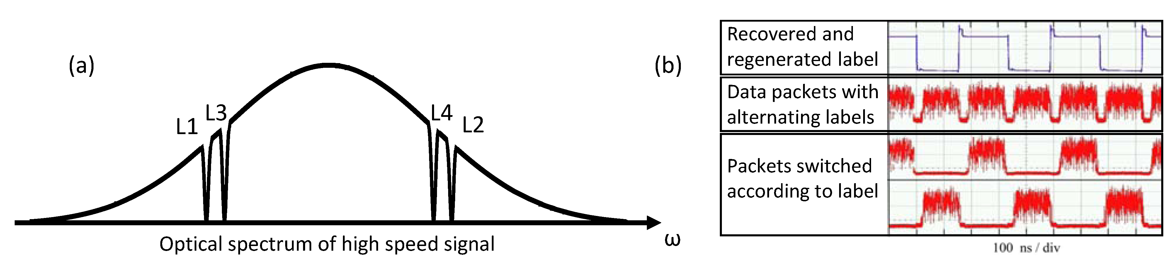
2.1. Principle of in-Band Optical Packet Labeling
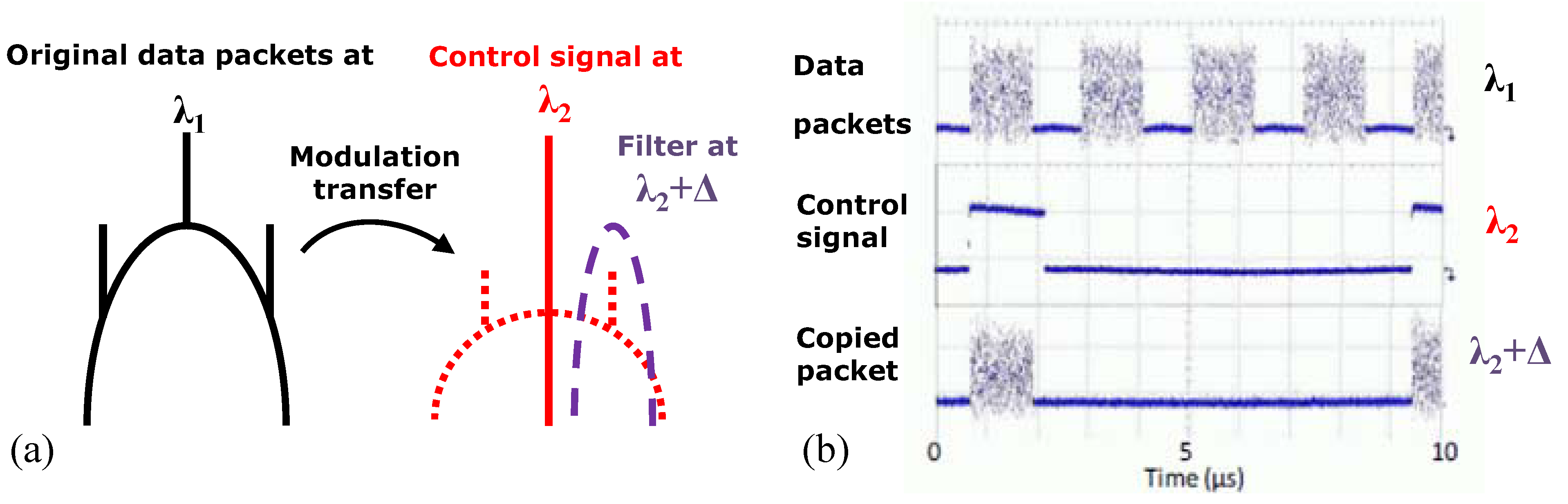
2.2. Optical Labeling of TDM Data Channels

2.3. Optical Switching of Data Packets
2.4. Optical Packet Switching by Wavelength Conversion in a Si Waveguide

2.5. Optical Packet Switching in an Electro-Optic Switch
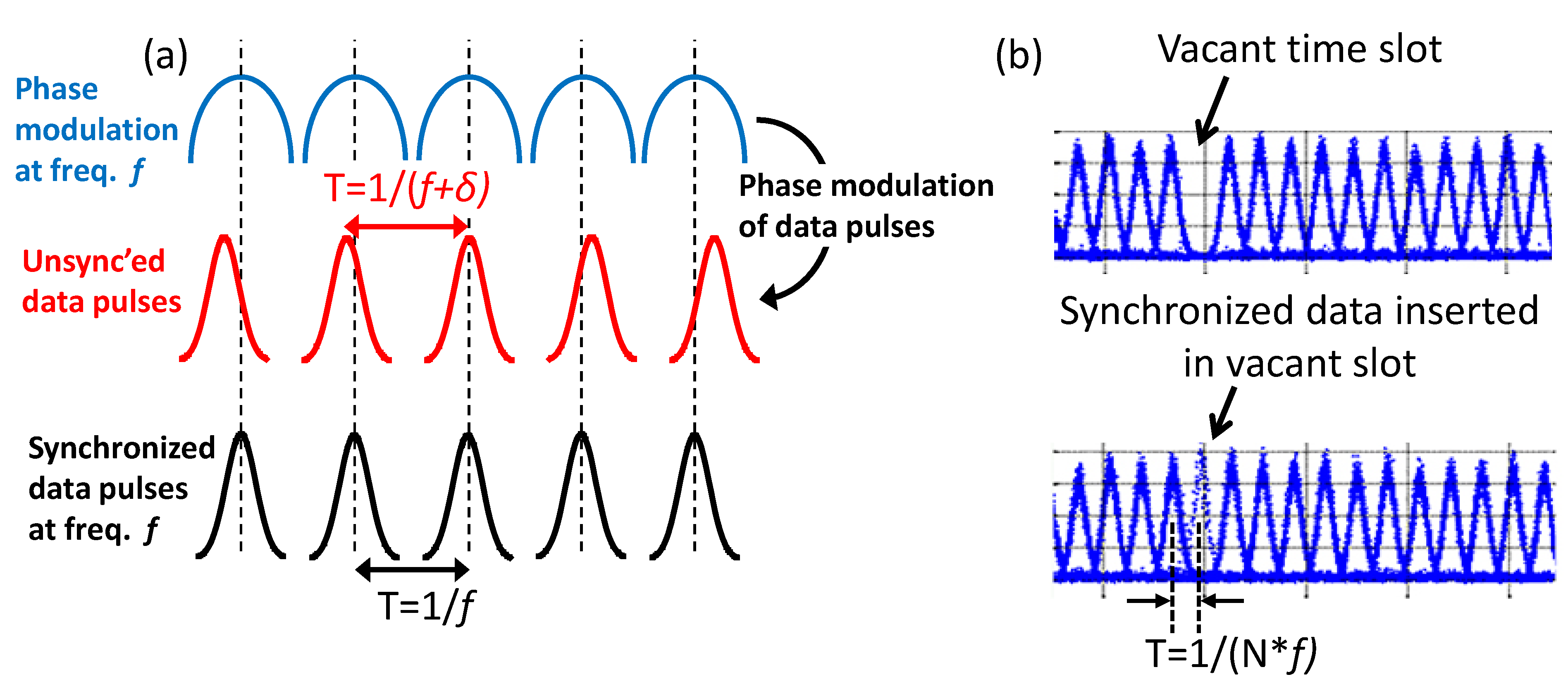
3. Optical Synchronization of Data Packets

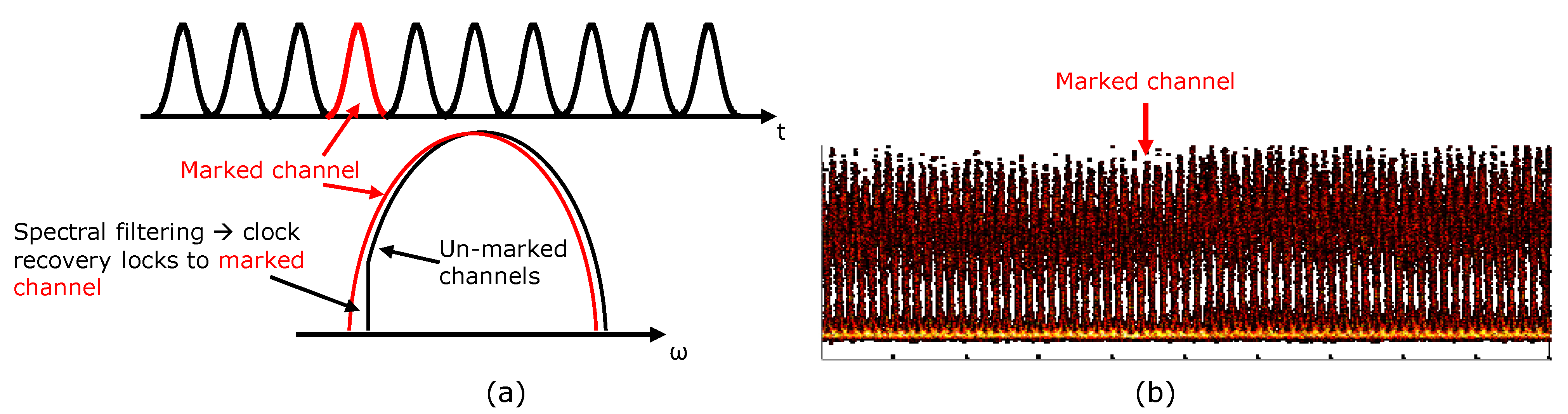
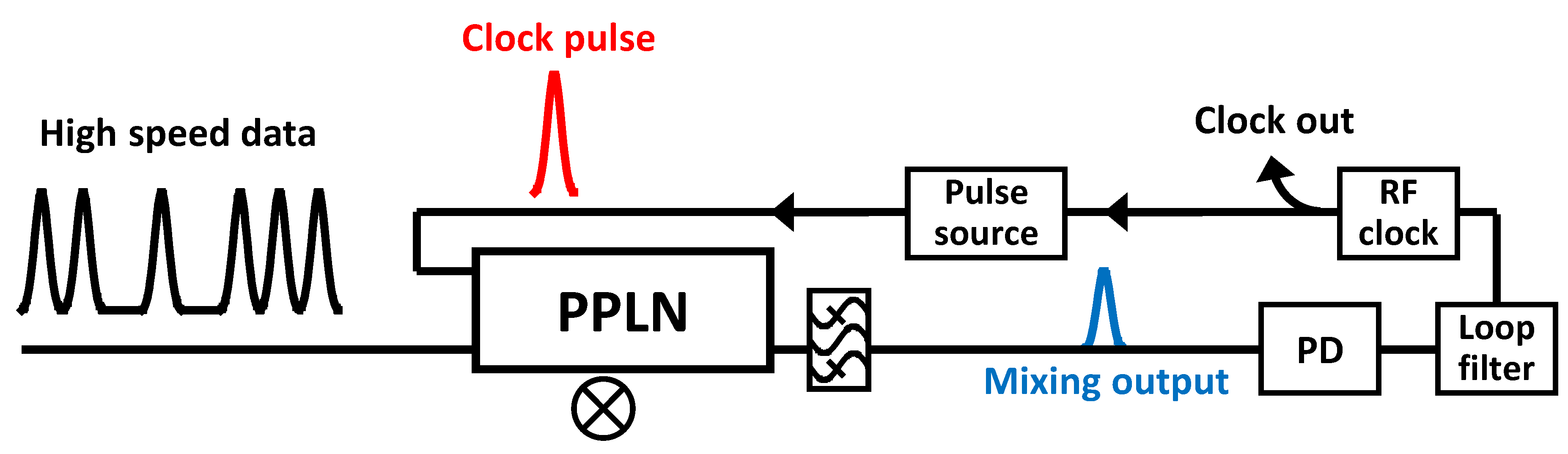
4. Ultra High Speed Clock Recovery
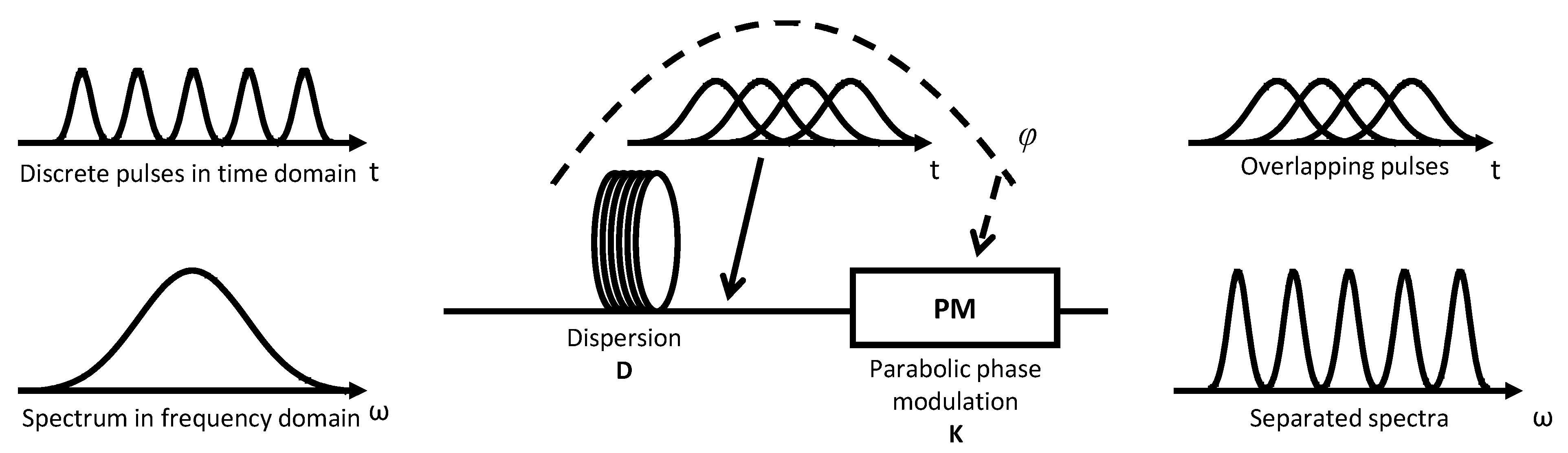
5. Efficient Detection of Ultra-High-Speed Data Signals
6. Discussion and Conclusions
Acknowledgments
Author Contributions
Conflicts of Interest
References
- Namiki, S.; Hasama, T.; Ishikawa, H. Optical signal processing for energy-efficient dynamic optical path networks. In Proceedings of the 36th European Conference and Exhibition on Optical Communication (ECOC), Torino, Italy, 19–23 September 2010; pp. 1–6.
- Tucker, R.S. Optical packet-switched wdm networks—A cost and energy perspective. In Proceedings of the Optical Fiber Communication Conference (OFC), San Diego, CA, USA, 24–28 February 2008. paper OMG1.
- Mehdin, A.K.; Galili, M.; Oxenløwe, L.K. Novel Optical Labeling Scheme for Ultra-High Bit Rate Data Packets. In Proceedings of the OptoElectronics and Communications Conference (OECC), Kyoto, Japan, 30 June 2013–4 July 2013; pp. 1–2.
- Medhin, A.K.; Galili, M.; Oxenløwe, L.K. 640 Gbit/s optical packet switching using a novel in-band optical notch-filter labeling scheme. In Proceedings of the Optical Fiber Communication Conference (OFC), San Francisco, CA, USA, 9–13 March 2014.
- Gomez-Agis, F.; Hu, H.; Luo, J.; Hansen Mulvad, H.C.; Galili, M.; Calabretta, N.; Oxenløwe, L.K.; Dorren, H.; Jeppesen, P. Optical switching and detection of 640 Gbits/s optical time-division multiplexed data packets transmitted over 50 km of fiber. Opt. Lett. 2011, 36, 3473–3475. [Google Scholar] [CrossRef]
- Galili, M.; Hansen Mulvad, H.C.; Hu, H.; Oxenløwe, L.K.; Gomez-Agis, F.; Ware, C.; Erasme, D.; Clausen, A.; Jeppesen, P. 650 Gbit/s OTDM Transmission over 80 km SSMF Incorporating Clock Recovery, Channel Identification and Demultiplexing in a Polarisation Insensitive Receiver. In Proceedings of the Optical Fiber Communication Conference (OFC), San Diego, CA, USA, 21–25 March 2010; pp. 1–3.
- Hu, H.; Galili, M.; Pu, M.; Yvind, K.; Jeppesen, P.; Oxenløwe, L.K. 160 Gbit/s optical packet switching using a silicon chip. In Proceedings of the IEEE Photonics Conference, Burlingame, CA, USA, 23–27 September 2012; pp. 915–916.
- Varrazza, R.; Djordjevic, I.B.; Yu, S. Active Vertical-Coupler-Based Optical Crosspoint Switch Matrix for Optical Packet-Switching Applications. J. Lightw. Technol. 2004, 22, 2034–2042. [Google Scholar] [CrossRef]
- Hu, H.; Areal, J.L.; Hansen Mulvad, H.C.; Galili, M.; Dalgaard, K.; Palushani, E.; Clausen, A.; Berger, M.S.; Jeppesen, P.; Oxenløwe, L.K. Synchronization, retiming and time-division multiplexing of an asynchronous 10 Gigabit NRZ Ethernet packet to terabit Ethernet. Opt. Express 2011, 19, B931–B937. [Google Scholar] [CrossRef]
- Hu, H.; Areal, J.L.; Palushani, E.; Oxenløwe, L.K.; Clausen, A.; Berger, M.S.; Jeppesen, P. Optical Synchronization of a 10-G Ethernet Packet and Time-Division Multiplexing to a 50-Gb/s Signal Using an Optical Time Lens. IEEE Photonics Technol. Lett. 2010, 22, 1583–1585. [Google Scholar] [CrossRef]
- Galili, M.; Oxenløwe, L.K.; Hansen Mulvad, H.C.; Clausen, A.T.; Jeppesen, P. Optical wavelength conversion by cross-phase modulation of data signals up to 640 Gb/s. J. Sel. Top. Quantum Electron. 2008, 14, 573–578. [Google Scholar] [CrossRef]
- Hansen Mulvad, H.C.; Tangdiongga, E.; Waardt, H.d.; Dorren, H. 40 GHz clock recovery from 640 Gbit/s OTDM signal using SOA-based phase comparator. Electron. Lett. 2008, 44, 146–148. [Google Scholar] [CrossRef]
- Oxenløwe, L.K.; Gomez Agis, F.; Ware, C.; Kurimura, S.; Hansen Mulvad, H.C.; Galili, M.; Kitamura, K.; Nakajima, H.; Ichikawa, J.; Erasme, D.; et al. 640 Gbit/s clock recovery using periodically poled lithium niobate. Electron. Lett. 2008, 44, 370–372. [Google Scholar] [CrossRef]
- Oxenløwe, L.K.; Gómez-Agis, F.; Ware, C.; Kurimura, S.; Hansen Mulvad, H.C.; Galili, M.; Nakajima, H.; Ichikawa, J.; Erasme, D.; Clausen, A.T.; et al. 640-Gbit/s Data Transmission and Clock Recovery Using an Ultrafast Periodically Poled Lithium Niobate Device. J. Lightw. Technol. 2009, 27, 205–213. [Google Scholar] [CrossRef]
- Hansen Mulvad, H.C.; Oxenløwe, L.K.; Galili, M.; Grüner-Nielsen, L.; Jeppesen, P. 1.28 Tbit/s single-polarisation serial OOK optical data generation and demultiplexing. Electron. Lett. 2009, 45, 280–281. [Google Scholar] [CrossRef]
- Hansen Mulvad, H.C.; Palushani, E.; Hu, H.; Ji, H.; Lillieholm, M.; Galili, M.; Clausen, A.T.; Pu, M.; Yvind, K.; Hvam, J.M.; et al. Ultra-high-speed optical serial-to-parallel data conversion by time-domain optical Fourier transformation in a silicon nanowire. Opt. Express 2011, 19, B825–B835. [Google Scholar] [CrossRef]
- Lillieholm, M.; Hansen Mulvad, H.C.; Palushani, E.; Peucheret, C.; Jeppesen, P.; Oxenløwe, L.K. Numerical investigation of power requirements for ultra-high-speed serial-to-parallel conversion. In Proceedings of the IEEE Photonics Conference (IPC), Burlingame, CA, USA, 23–27 September 2012; pp. 110–111.
- Hu, H.; Kong, D.; Palushani, E.; Andersen, J.D.; Rasmussen, A.; Sørensen, B.M.; Galili, M.; Hansen Mulvad, H.C.; Larsen, K.J.; Forchhammer, S.; et al. 1.28 Tbaud Nyquist Signal Transmission using Time-Domain Optical Fourier Transformation based Receiver. In Proceedings of the Conference on Lasers and Electro-Optics (CLEO), San Jose, CA, USA, 9–14 June 2013.
- Petrillo, K.G.; Foster, M.A. Full 160-Gb/s OTDM to 16x10-Gb/s WDM conversion with a single nonlinear interaction. Opt. Express 2013, 21, 508–518. [Google Scholar] [CrossRef]
© 2014 by the authors; licensee MDPI, Basel, Switzerland. This article is an open access article distributed under the terms and conditions of the Creative Commons Attribution license (http://creativecommons.org/licenses/by/3.0/).
Share and Cite
Galili, M.; Hu, H.; Mulvad, H.C.H.; Medhin, A.K.; Clausen, A.; Oxenløwe, L.K. Optical Systems for Ultra-High-Speed TDM Networking. Photonics 2014, 1, 83-94. https://doi.org/10.3390/photonics1020083
Galili M, Hu H, Mulvad HCH, Medhin AK, Clausen A, Oxenløwe LK. Optical Systems for Ultra-High-Speed TDM Networking. Photonics. 2014; 1(2):83-94. https://doi.org/10.3390/photonics1020083
Chicago/Turabian StyleGalili, Michael, Hao Hu, Hans Christian Hansen Mulvad, Ashenafi Kiros Medhin, Anders Clausen, and Leif Katsuo Oxenløwe. 2014. "Optical Systems for Ultra-High-Speed TDM Networking" Photonics 1, no. 2: 83-94. https://doi.org/10.3390/photonics1020083
APA StyleGalili, M., Hu, H., Mulvad, H. C. H., Medhin, A. K., Clausen, A., & Oxenløwe, L. K. (2014). Optical Systems for Ultra-High-Speed TDM Networking. Photonics, 1(2), 83-94. https://doi.org/10.3390/photonics1020083