Algebraic Operations on Delta-Sigma Bit-Streams


Institut für Regelungstechnik, Technische Universität Braunschweig, 38106 Braunschweig, Germany
*
Author to whom correspondence should be addressed.
†
Current address: Hans-Sommer-Str. 66, 38106 Braunschweig.
Math. Comput. Appl. 2018, 23(3), 49; https://doi.org/10.3390/mca23030049
Submission received: 15 August 2018
/
Revised: 30 August 2018
/
Accepted: 3 September 2018
/
Published: 10 September 2018
(This article belongs to the Section Engineering)
Abstract
:Operations in the Delta-Sigma () domain are a broad field of research. In this article the main, focus is on applications in control systems, nevertheless the results are generally applicable for -signal processing (SP) in other fields. As the bit-stream does not have an instantaneous value, algebraic operations cannot be executed directly. The first approaches were made in the 1980s based on small-scale integration logic chips by Kouvaras and by Lagoyannis. Further algebraic operations and other implementations were introduced by Zrilic, by Ng, by Bradshaw and by Homann. Other publications utilize complex networks and operations to achieve the desired algebraic operations. These presented operations can be divided into different operation classes by the based implementation idea. In this paper, the known algebraic operation classes are further developed and new operation classes are presented. All implementations are compared and evaluated. For linear operations in control applications, the introduced Bipolar Interpretation is best rated. It compensates for the signal offset of bipolar bit-streams and results in the best signal quality by mapping the logic values true and false of bit-stream to plus and minus one before the algebraic operation. The output of the algebraic operation is a multibit value, to achieve a bit-stream as output value a third step is taken. The result is modulated by a digital -modulator (-M). For nonlinear operations the most universal implementation is also based on three steps. In the first stage, the bit-streams are processed with short sinc filters, resulting in multibit values. This signal is processed by digital signal processing (DSP). The output stage is a -M. For some nonlinear algebraic operations there can be better solutions than DSP, like shown for limiting. In short, this paper gives a detailed overview about different SP classes for linear and nonlinear operations. Newly presented are the scaling with Bit-Stream Modification, the Bipolar Interpretation class, the nonlinear operation class based on digital signal processing (DSP), the modified multiplication based on Delta Adder and benchmarks of all presented operations.
1. Introduction
The control of mechatronic systems is usually performed using time-discrete signal processing. The basic elements of time-discrete control are the analog-to-digital converter (ADC), the control law for processing the pulse series and a digital-to-analog converter (DAC) usually by pulse width modulation (PWM). The synchronous control ensures the equidistant execution of the control law and the correct temporal reference of the analog-to-digital conversion in relation to the PWM. Sampling and calculation times limit the small signal bandwidth of time-discrete control loops [1]. In addition, different clock domains often occur in modern control systems, since set point and actual values are more often transmitted via digital bus systems. The different clock rates of bus systems and digital controls as well as jitter caused by stochastic bus access require a synchronization of the data words. Analog-to-digital conversion of actual values such as current or position is frequently realized by oversampling ADCs to increase the effective resolution by filtering in a faster time frame. The filtering followed by decimation requires, as in bus systems, a synchronization of the data words. This is also stressed in [2], where it is demonstrated that the small signal bandwidth of a current control with Delta-Sigma () ADCs depends strongly on the correct sequence of the time discrete control.
The key indicators for the control loop performance are the small signal bandwidth and the control quality. In terms of small signal bandwidth, a purely analog current control in conjunction with a linear power amplifier is best rated. However, this approach is no longer being pursued in practice for various reasons. On the one side, the analog implementation of control laws is based on operational amplifiers. Thus, noise is superimposed on each stage, furthermore drift and parameter inaccuracies additionally worsen the signal quality. Moreover, complex functions (sine/cosine, square root, and overflow integrator) are hardly economically viable and stable over the long term.
In digital closed control loops, the sampling rate limits the small signal bandwidth. If ADCs are used in classical setup, the phase delay of the low-pass and decimation filter has to be added to the sampling time.
As a possible solution to these challenges, this publication provides an overview of a new type of signal processing. A high-frequency (≥ 10 ) sampling and signal processing for systems with low operation frequencies (≤ 1 ) enables a practically sample-free control as a hybrid between analog and digital signal processing. Set point and actual values of this signal processing are generated by -Ms, which are described in the following section. To bring the achieved small signal bandwidth of SP to effect, the high-frequency bit-streams into power semiconductor compatible switching frequencies. For example, in the field of electrical drives with a single phase drive, a -M with a hysteresis based quantizer can be used [3,4,5]. For a three phased drive, different strategies have been presented [4,5,6,7,8]. From these, the implementation based on [7] is preferred, as it is the only implementation realizing a true space vector modulation sequence resulting in the same switching frequencies for all phases, which leads to equal thermal stress. In combination with the presented operations complex control loops with a high small signal bandwidth can be realized.
2. Delta-Sigma Modulators
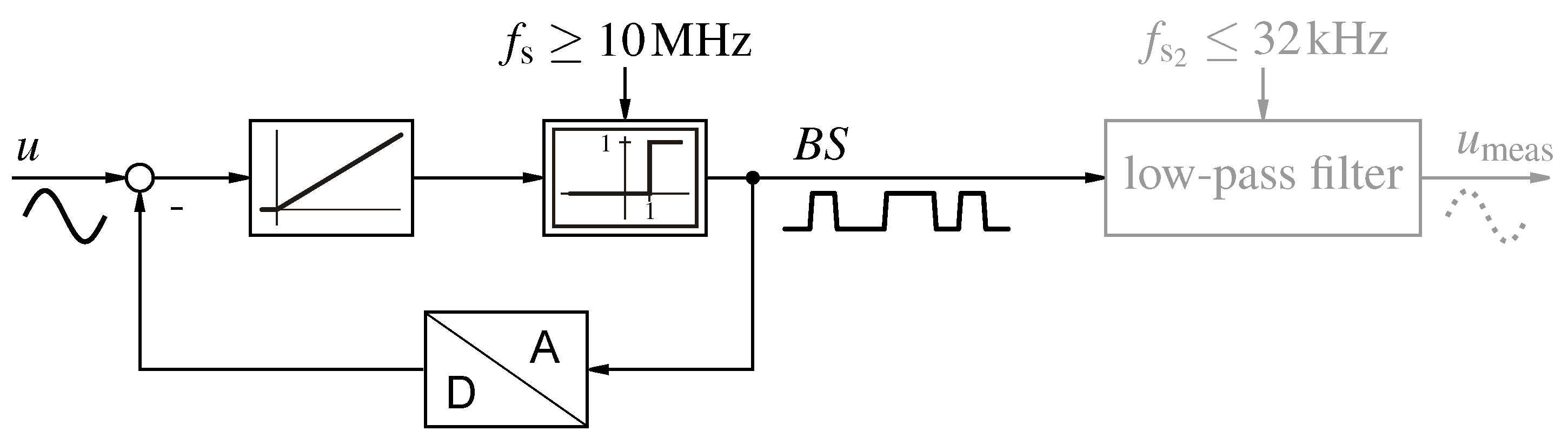
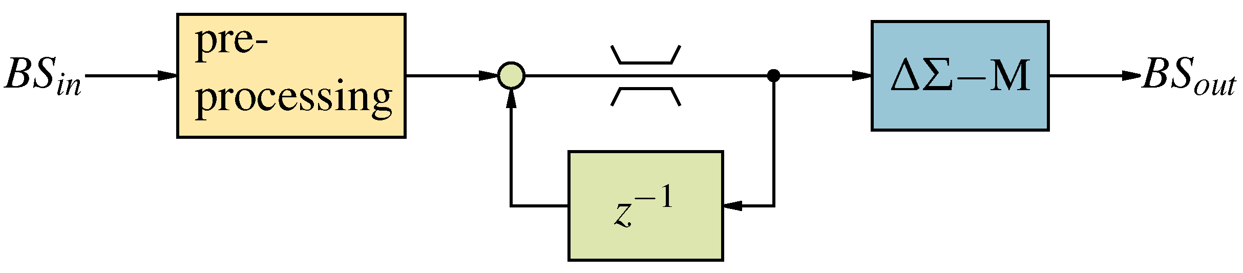
Signal processing based on bit-streams requires an understanding of the operation of -Ms. In a classical analog-to-digital conversion setup, a -analog-to-digital converter is comprised of two elements, i.e., the -M and a low-pass filter with decimation, as shown in Figure 1 [9,10]. By omitting the low pass filter and directly operating on the high frequency (≥ 10 ) bit-stream () [5,8,11,12,13], a larger small signal bandwidth is achieved, e.g., in control loops.
The -M consists of one or several integrators, a sampled comparator in a closed feedback loop with gains. The order of the -M is specified by the number of cascaded integrators, i.e., in Figure 1a first order -M is shown. While first order -Ms are always stable, for higher-order -Ms the feedback coefficients to individual stages have to be designed carefully to stabilize the feedback loops [10,14]. Several design methods are known from literature [9,10,15,16]. In this work second order -Ms as proposed in [16] and shown in Figure 2 are used.
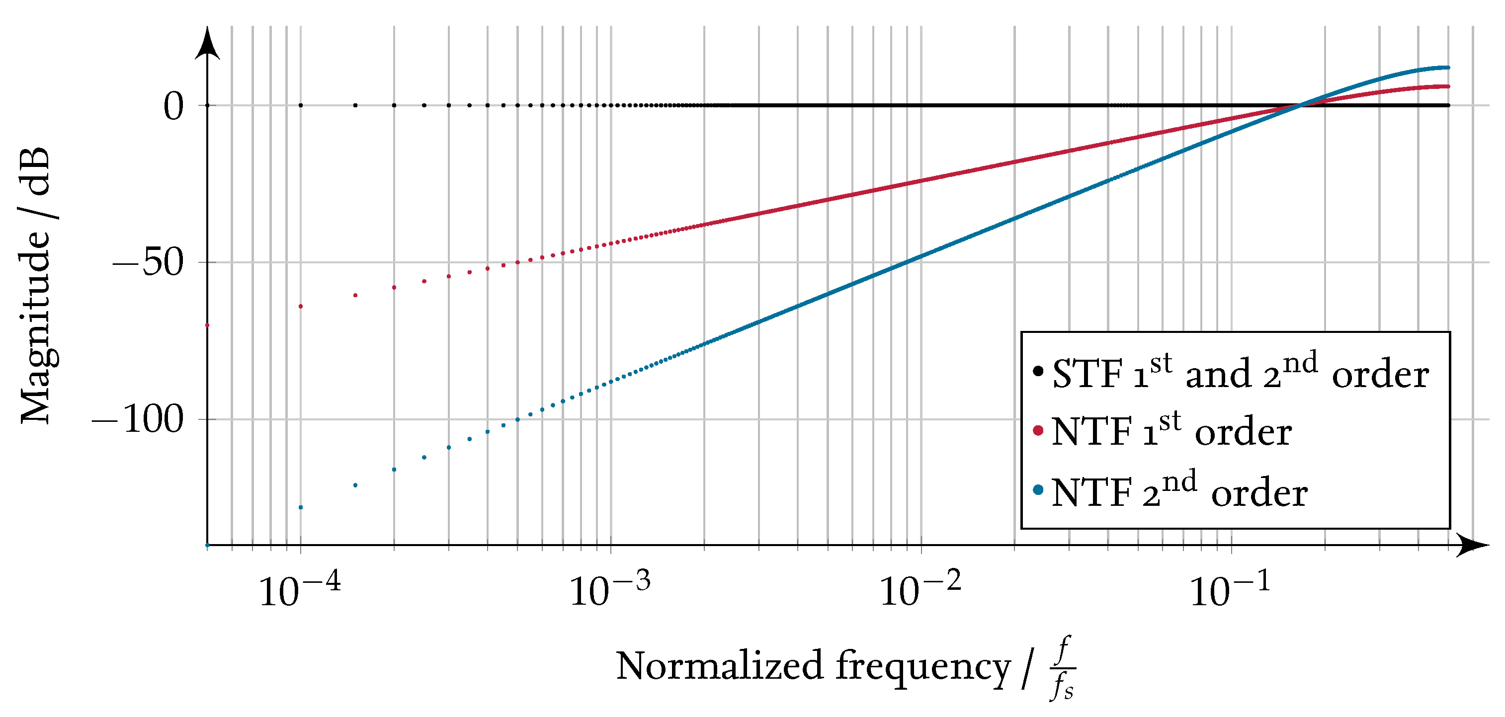
Considered as a closed control loop, the -M integrates the control error between the input signal and the output signal. If this integral is greater than zero, it outputs a one, else a zero for the next clock cycle. This simple control law ensures, in conjunction with the feedback loop, that the output bit-stream, only consisting of ones and zeros, represents the input signal in its average. As the bit-stream can only transport 1 bit information per clock cycle, quantization noise is introduced into the output bit-stream. Due to the internal structure, the -M provides noise shaping [10,11,14]. As shown in Figure 3, the quantization noise is mainly shifted to the high frequency signal components. In a classical DSP implementation, these are attenuated by a digital low-pass filter. In SP, the high frequent noise is retained in the bit-streams and thereby influences the local distribution of ones and zeros [17].
The -Ms can be implemented in two ways. In a hardware -M, the integrator is an analog circuit and the feedback is a one bit digital-analog-converter, whereas, in a digital -M, the whole modulator is implemented in software, converting a multibit input into a bit-stream.
In general, there are two obvious ways to map the logical values and , respectively, 1 and 0, to normalized signal values: signed and unsigned. In the signed case, the logical 1 is mapped to 1 and the logical 0 is mapped to , whereas, in the unsigned case, the logical 0 is mapped to 0. In control system applications usually the signed interpretation is used. Thus, it is assumed that the 0 represents a .
3. Linear Operations in Delta-Sigma Signal Processing
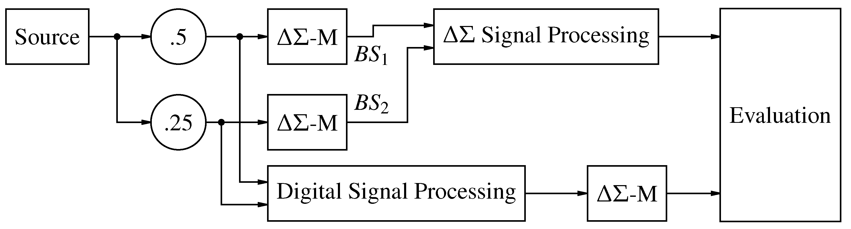
In the literature, many operation classes for -modulated signals are presented [4,5,18,19,20,21]. Other classes are sorting network based operations [22], 1-bit CORDIC algorithm based on [23] and sinc-filtered multibit operations [5]. In this article, the focus is on the -M based operations, as shown in Figure 4.
The main problem for linear operations is that the signal is transformed by the bit-stream encoding, as the bipolar input is projected to the bit-stream containing only ones and zeros . Thus, ones in the bit-stream represent the information (v) in dependence of the represented signal (u) and a fixed offset (o), which can be described as
The fixed offset is a problem for linear operations, as it is defined as for a bipolar bit-stream [4,11]. In the addition of two bit-streams, as an example, the offset of one bit-stream fulfills the required offset for the output bit-stream and the offset of the other input bit-stream is interpret as signal component resulting in the addition of one normalized unit. This will probably overdrive the output bit-stream and falsifies the represented value. In the case of a scaling operation, the offset is scaled with the same factor as the signal part. This results in an additional subtracting of the inverse scaling factor for scaling factors smaller than one and an addition for scaling factors greater one.
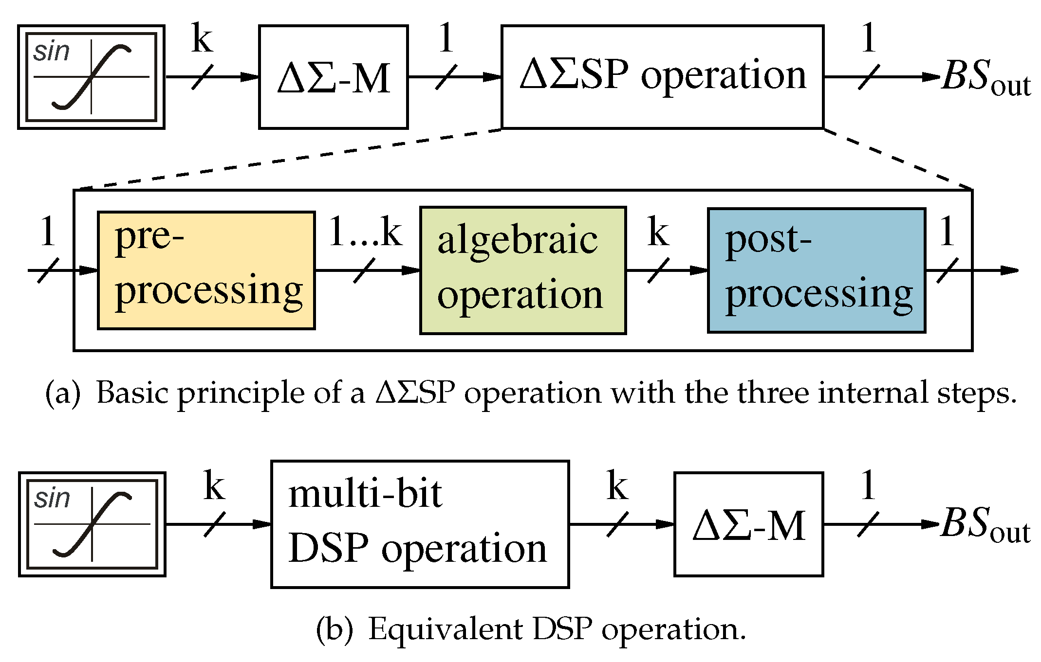
To cope with the offset, different SP strategies have been developed. One class of SP are the -M based operations, which consist of a possible preparation step, which handles the offset, the arithmetic operation and a -M to output a bit-stream. In some implementations, e.g. based on Delta Adders, some steps can be omitted or are hidden and can be revealed by transformation into control system structures.
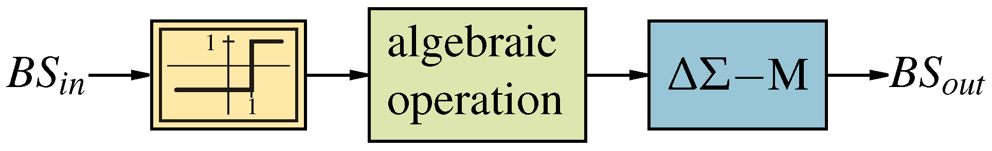
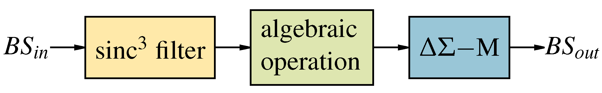
The basic idea is to modify the bit-stream in the way that the represented value correlates to result of a classical multibit DSP or analog operation. Usually, three processing steps, shown in Figure 4a, are taken to execute the transformation. In the first, the incoming bit-stream is prepared for the operation, depending on the utilized operation class, leading to a 1 to k bit value. In the next step, the arithmetic operation is performed usually resulting in a multibit value. In the last step, the multibit result is transformed into a one bit signal, the output bit-stream.
3.1. Delta Adder
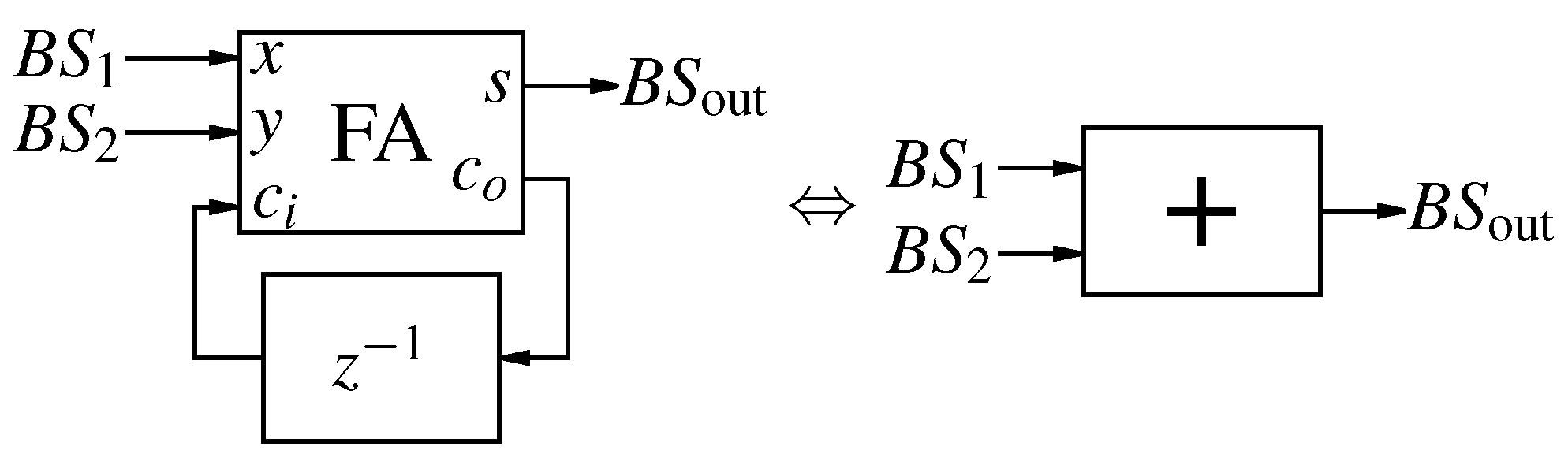
The earliest method for performing calculations with bit streams is based on a full adder (FA) and delay logic [18]. As shown in [11,24], the operation is equivalent to an addition with division by two and subsequent modulation with a first order -M. The division by two corrects the offset, as the half of two offsets of bit-streams results in the correct offset from Equation (1) in the output bit-stream, this can be expressed by
The classical implementation in logic cells is shown in Figure 5 and the corresponding control scheme is shown in Figure 6.
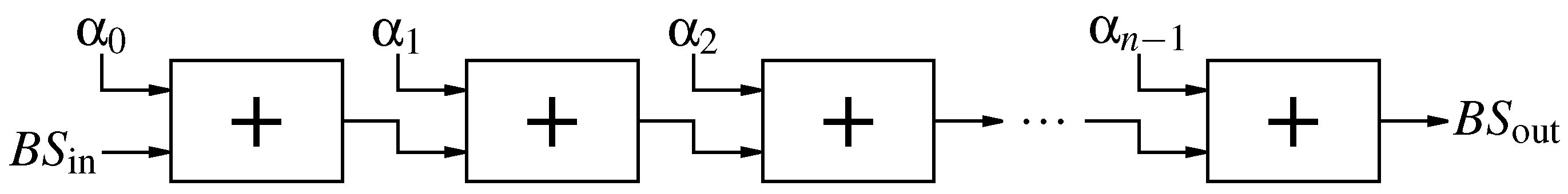
Based on this technology, a multiplication with a multibit integer fractional constant for scaling factors has been presented [18]. The scaler is based on the inherent division by two of the delta adder. Thus, the scaling is achieved by a cascade of delta adders with one constant input to a high or a low value representing the scaling factor in binary notation, as shown in Figure 7.
According to the implementation, the number of Delta Adders used by this technique for one operation scales linearly with the bit width (n) of . is the most significant bit (MSB) and is the least significant bit (LSB) of the scaling factor. The resulting function can be expressed for the represented value as follows
3.2. Bit-Stream Modification
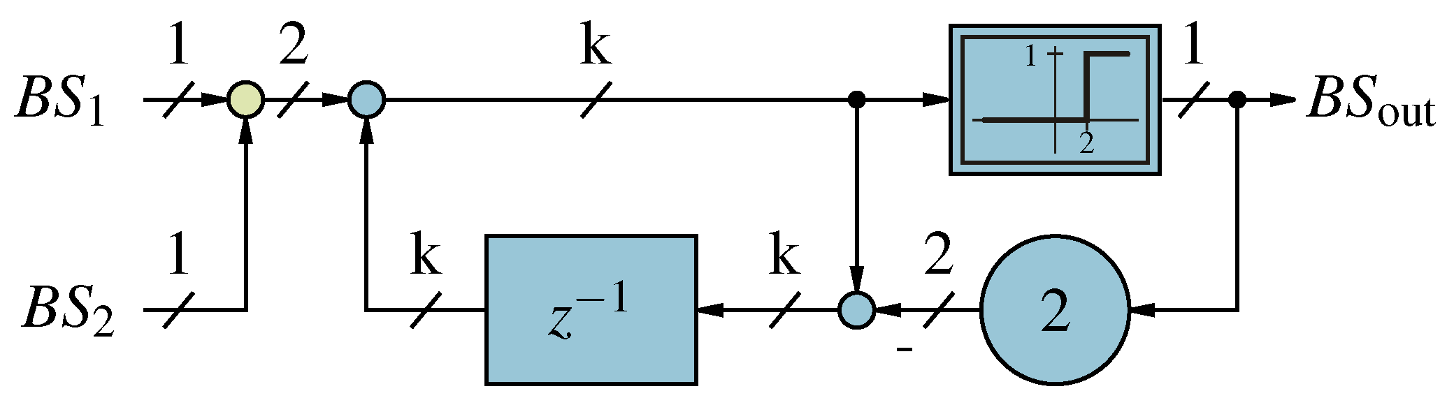
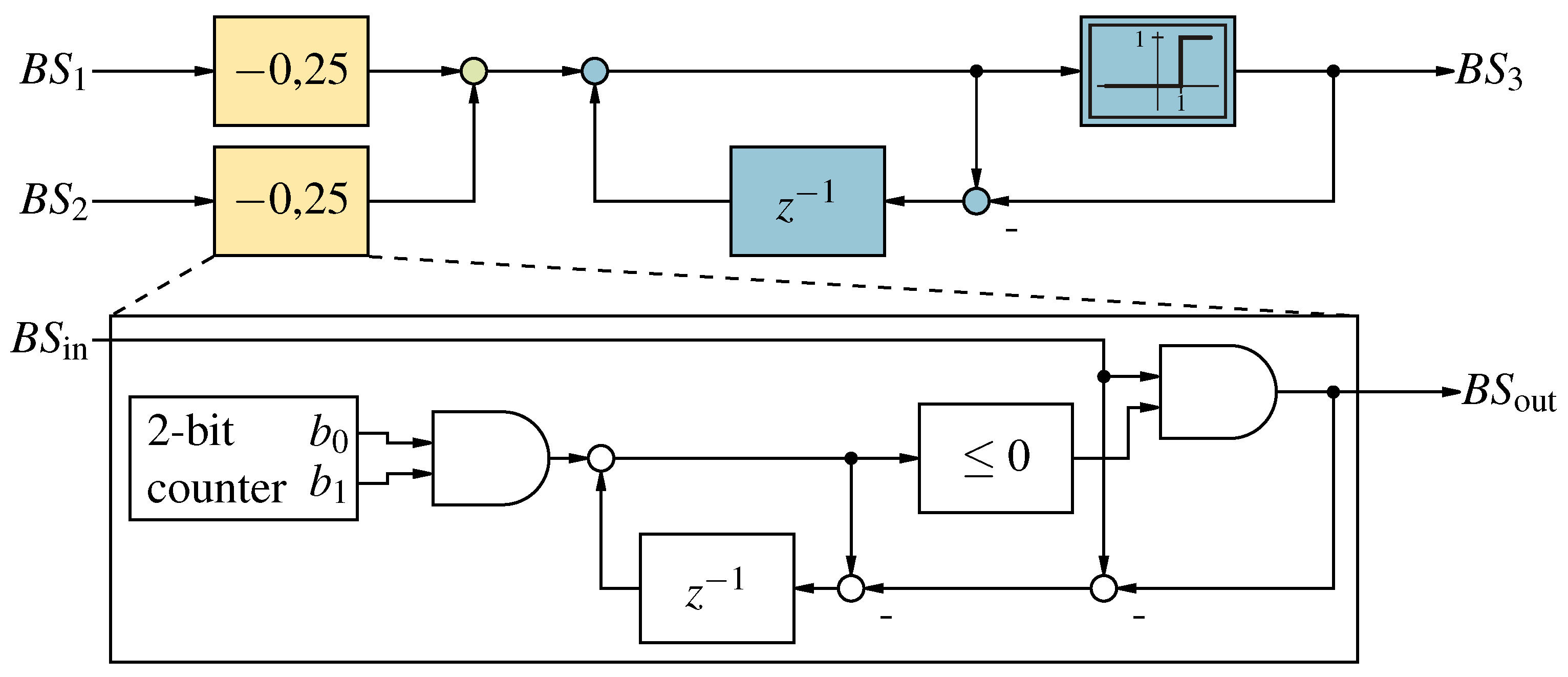
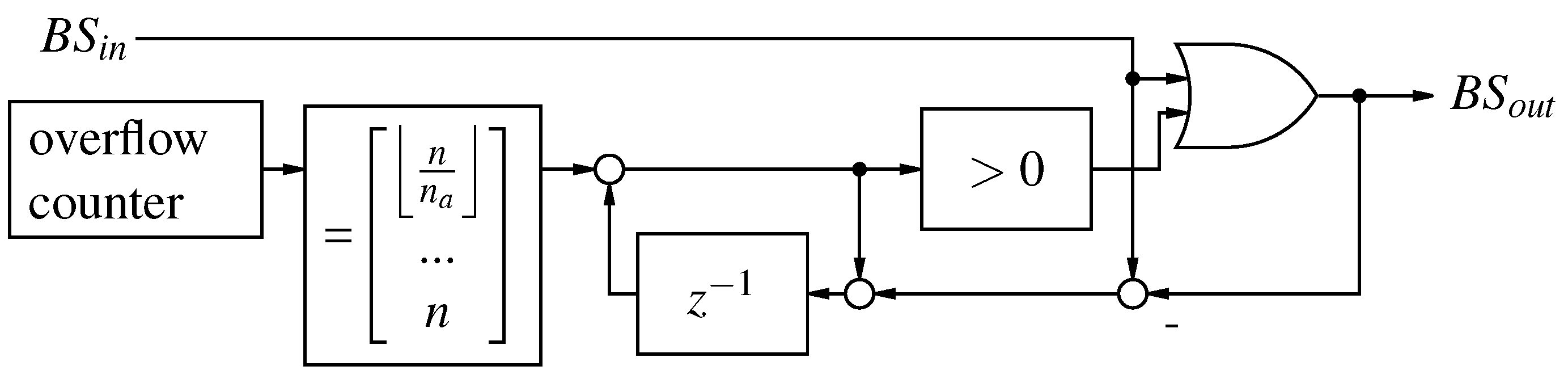
Another technology presented in the literature is the bit-stream modification [5]. It is based on the idea that the signal in the bit-stream consists of two parts, the signal part and the constant offset. The addition in bit-stream modification can be represented as a subtraction of the fixed value , an addition and a storage for excess ones. These ones are generated if two ones should be output concurrently, for instance if both input bit-streams are one and none of both is changed to zero. The storage is a modified first order -M [5]. To subtract 0.25, each forth clock cycle a one is transformed into a zero in the bit-stream. If the bit-stream is zero, the next one will be transformed. Figure 8 shows the detailed block diagram. This results in a section length (n) of four with one comparison. The subtraction of the fixed value for both input bit-streams results in the correct fixed offset from (1) in the output bit-stream, as follows
Scaling operations can also be performed by bit-stream modification. To retain the fixed offset, additional logic has to be implemented.
For a scaling factor greater than one, the fixed offset, defined in Equation (1), is also upscaled, thus ones have to be converted to zeros in the bit-stream to ensure the correct offset. To avoid an overflow during the operation, the ones should be converted before the scaling operation, otherwise a scaling of two would be the maximum factor for zero input. The amount of converted ones () can be derived from the scaling factor (s) and the section length (n) as follows
For a scaling factor less than one, the fixed offset, defined in Equation (1), is downscaled, thus zeros have to be converted into ones in the bit-stream to ensure the correct offset. In order not to produce an overflow during the operation, the zeros should be converted in the output bit-stream. The amount of zeros converted () can be derived from the scaling factor (s) and the section length (n)
With this information, the minimal section length (n) can be calculated, which results in a natural number for the altered bits ( [stands for or ]). A good implementation distributes the altered bits evenly in the section. This can be achieved by an overflow counter with the length n and comparisons. The implementation for reducing the amount of ones can be similar to −0.25 in Figure 8, only with a modified counter length (n) and comparisons instead of the logic operation AND (AND) at the counter output. To add ones, the control structure has to be adjusted. In Figure 9, the required structure is shown. The compare block outputs a one, if the input value is in the list.
3.3. Counter Based
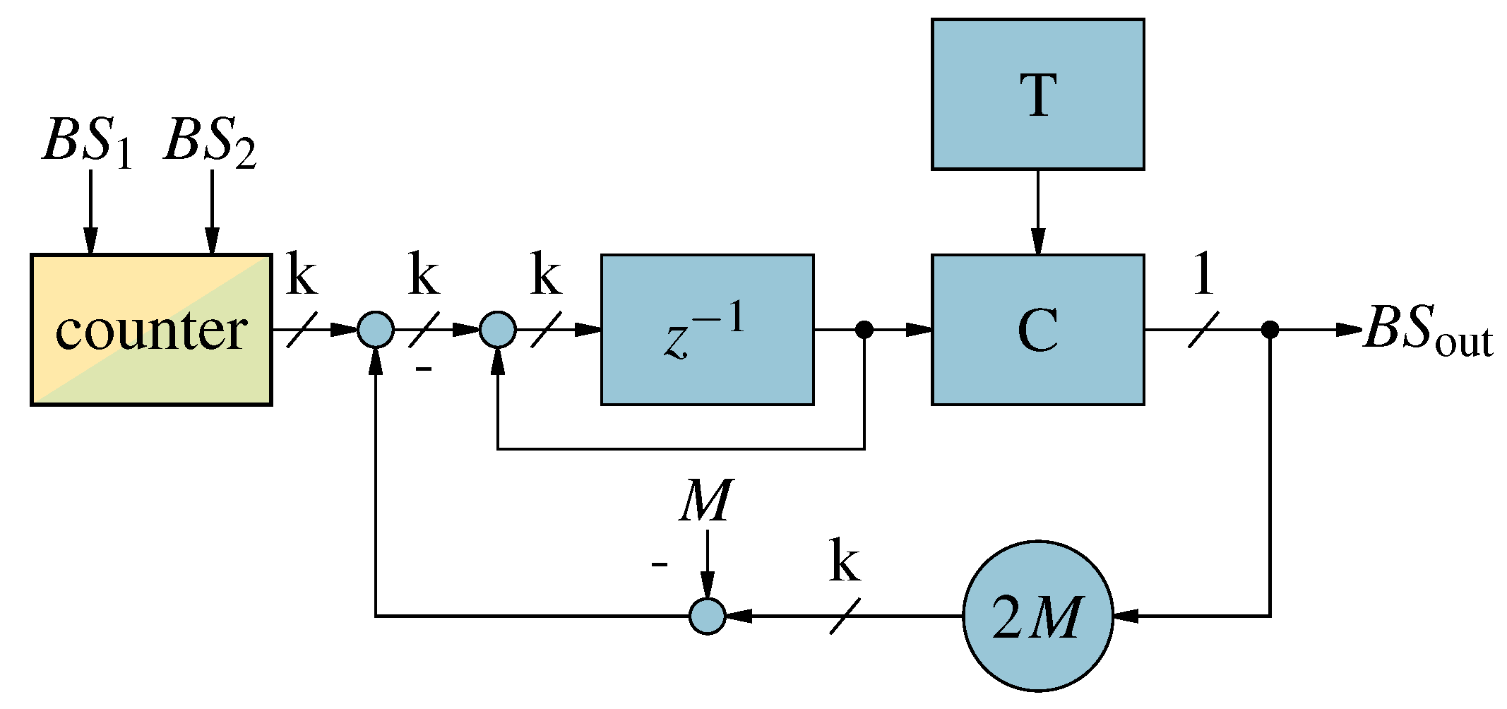
Another approach is based on counters [20]. The constant offset is removed at the input stage by a counter summing up all inputs twice and subtract the count of inputs, resulting in
This results in the same preparation, as the Bipolar Interpretation in Section 3.6. The output stage is formed by a modified -M. In this overview, the adder and the combination of the adder and the second order average adder are investigated. The first order adder is shown in Figure 10.
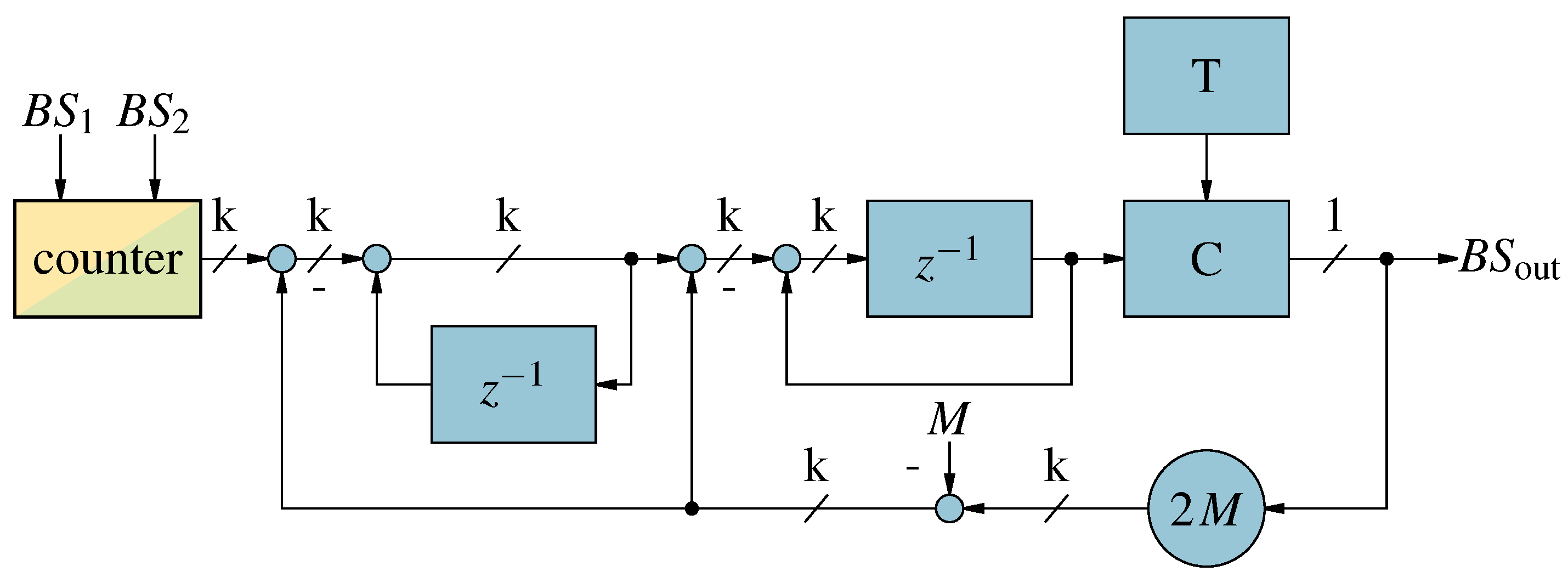
The second order adder is achieved by setting the feedback coefficient (M) to 1 instead of the count of input bit-streams. This results in the topology shown in Figure 11.
The modification to a general -M is the implemented quantizer. For inputs smaller than zero, it outputs a zero and for inputs greater than zero, it outputs a one. This is the common behavior of a two state quantizer utilized in a -M. For inputs equal zero, the additional logic T comes in action. It outputs alternating ones and zeros, toggling each time pulled. The truth table is given in Table 1.
Based on this adder, an average adder is developed, by setting the feedback scaling factor M to the count of inputs. The average adder can be utilized to downscale a signal. If m of the inputs are connected to the signal and inputs are connected to the bit-stream of a zero signal (, which is introduced in Section 3.4). Thus, a scaling by is achieved. For implementation reasons, is required. If the postulated requirement is omitted, scaling factors for upscaling and downscaling can be implemented. For upscaling, operation precautions have to be taken, in order not to overdrive the bit-stream.
3.4. Quanta Decoding
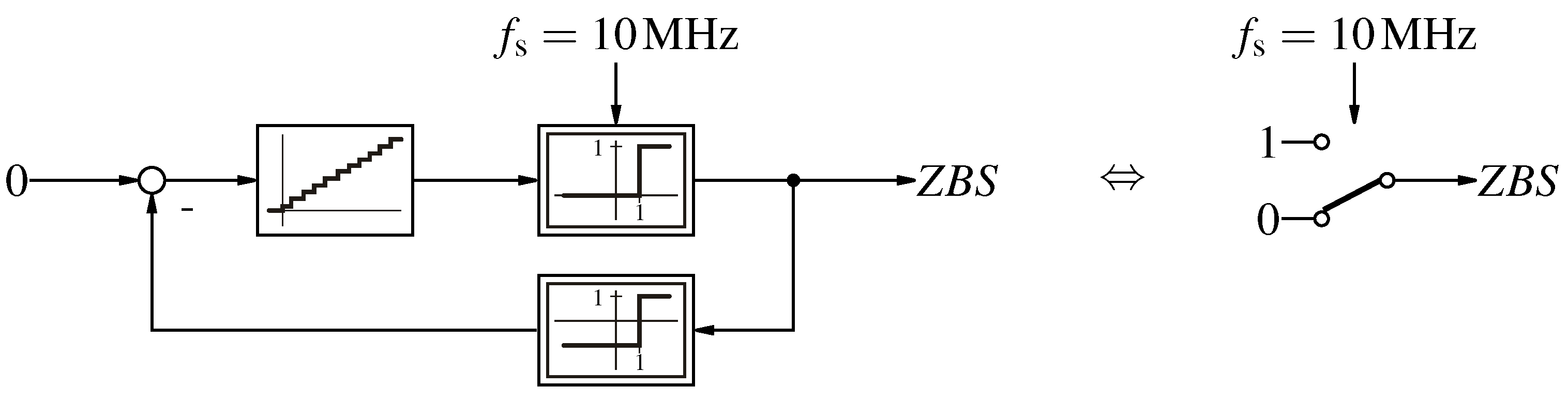
The operation class with the highest signal-to-noise and distortion ratio (SINAD), which is known from literature, is Quanta Decoding [11,21,25]. For this operation class, a so-called “zero bit-stream” (ZBS) is utilized to remove the constant offset. The ZBS is the output of a bipolar first order -M with a zero input signal. This results in a bit-stream consisting of alternating ones and zeros, which is equivalent to a clocked switch, as shown in Figure 12, or a frequency divider by two. For implementation purposes the latter two options are preferred.
The ZBS is subtracted from each input signal. This leads to the truth table Table 2. The quanta (±Q) are interpreted as ±1, resulting in a ternary signal.
To regain the constant offset after the arithmetic operation, the result is modulated with a bipolar -M. For the operation addition, the offset is resulting in
The division by two, shown in Equation (1), can be compensated for by scaling with the factor two.
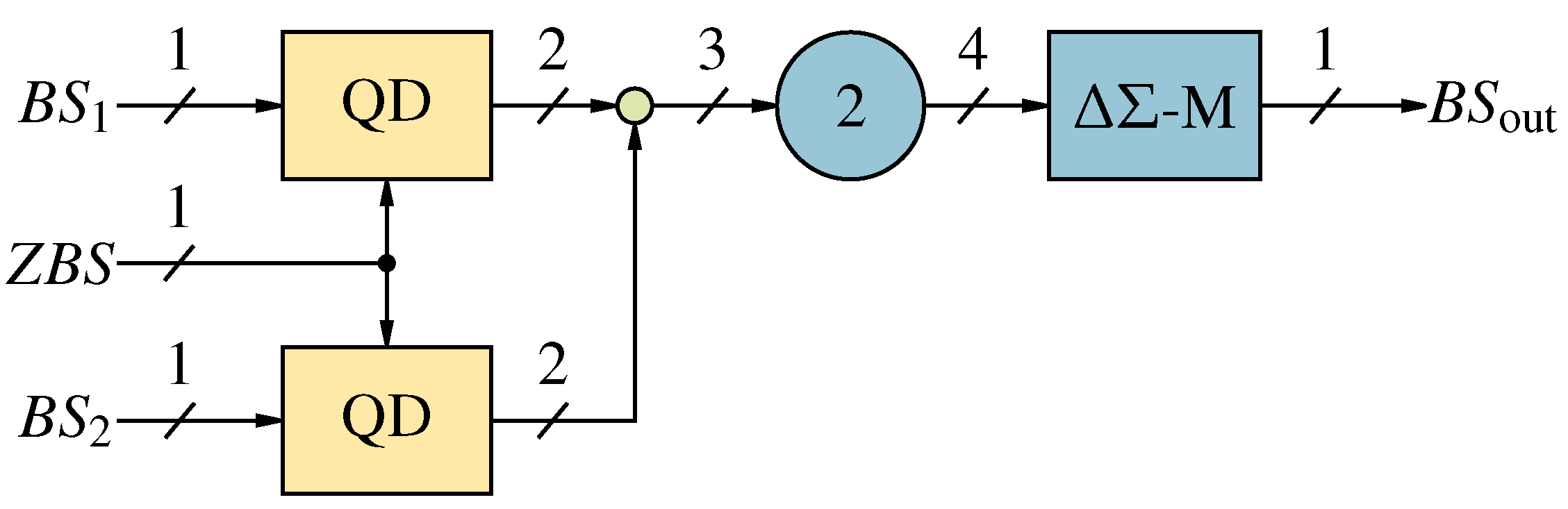
For example, the operation addition implemented in Quanta Decoding is shown in Figure 13.
As the constant offset is removed from the bit-stream in the first stage of the operation and added at the last stage, scaling operations can be performed without additional precautions.
The drawback of this solution is the noise introduced by the so called ZBS. It can be reduced by using a higher order -M to generate the ZBS. The disadvantage of that solution is that it takes more logic elements to implement the extra -M.
3.5. Advanced Quanta Decoding
An enhanced version of Quanta Decoding is Advanced Quanta Decoding. This operation class neglects the ZBS and thereby the additional noise. The drawback of this operation class is that it can only be implemented if the linear algebraic operation can be expressed as the difference of an even count of signals as first stage. For the offset results,
The resulting bit-stream is similar to the bit-stream if both input signals are first quanta decoded with the same ZBS and then the difference is calculated. This can be seen in Table 3, the logic table for two ZBS and two input bit-streams (BS) as operation input. In the next columns, the quanta decoded values (QD) of the bit-streams and the corresponding ZBS are shown. In the last columns, the result of the algebraic operations subtraction (−) and addition (+) are shown for the quanta decoded values, such as classical Quanta Decoding and the direct processed bit-streams. As can be seen, in the highlighted rows, where the used ZBS are equal, the results for the algebraic operation minus are the same with and without Quanta Decoding.
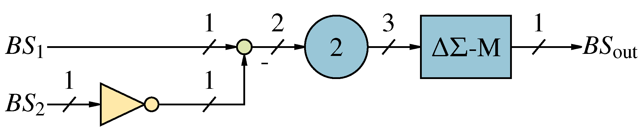
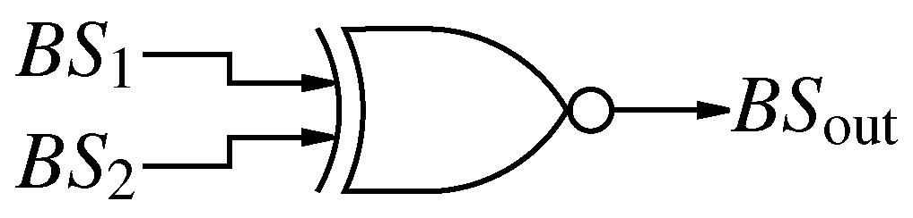
For the algebraic operation addition, the results with and without Quanta Decoding differ in some cases. Considering the logic operation NOT (NOT) results in an inversion of the bipolar bit-stream [26], each addition can be converted to a subtraction, as shown in Figure 14. In control circuits usually the control error is calculated as first operation, thus Advanced Quanta Decoding is a good compromise for SP in control applications. For an uneven count of input signals, one ZBS can be added as input. This leads to a combination of Advanced and classical Quanta Decoding.
3.6. Bipolar Interpretation
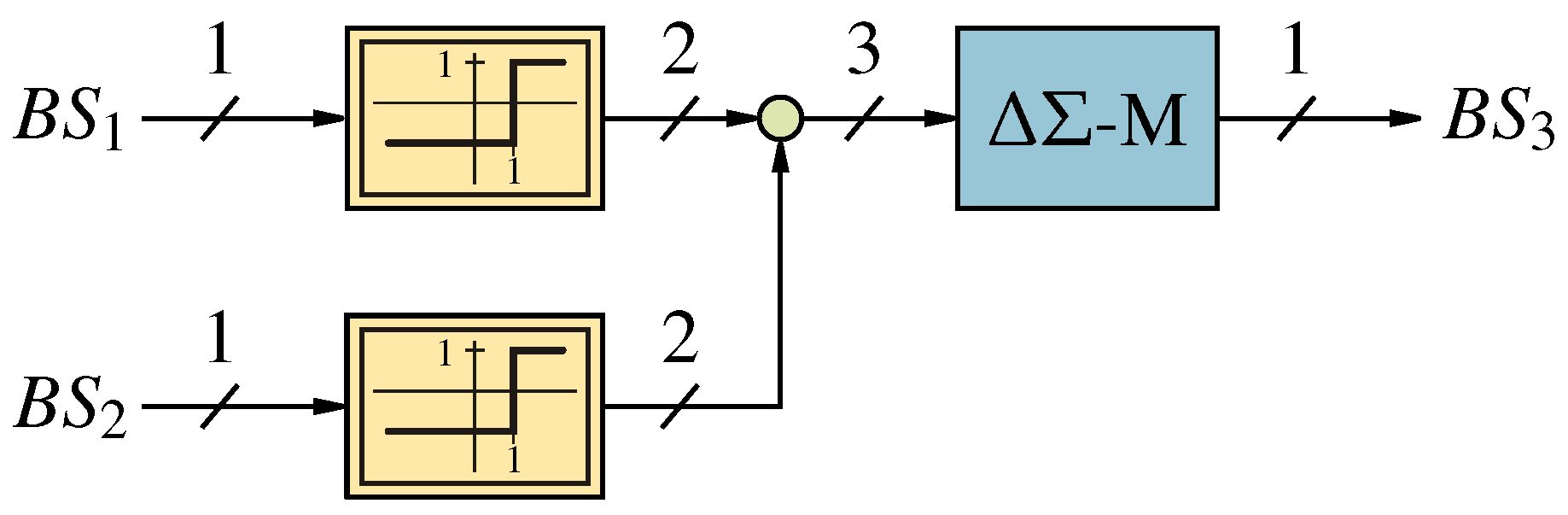
For all purposes, where SP should be used and there is an uneven number of signals used in the first operation, a new operation class has to be developed. The problem faced by Bit-stream Modification and Quanta Decoding is the offset in the bipolar bit-streams. This offset can be reduced to zero, if the Bipolar Interpretation of the bit-stream is made before an algebraic operation is performed. Therefore, a one in the bit-stream is mapped to the value one and a zero in the bit-stream is mapped to the value minus one before the operation is applied. The offset is described by
The fundamental operation can be seen in Figure 15. This mathematical definition eliminates the parasitic offset. The great advantage is that this operation class is not limited to an even count of input signals or additional zero signals, such as the ZBS. In comparison to Quanta Decoding, the inherent division by two is also dropped. The input and the output bit-stream can be a bit-stream vector. In the case of an output bit-stream vector, multiple -Ms are requested. In the case of an input vector, each bit-stream is mapped individually, as shown for the algebraic operation addition in Figure 16.
3.7. Evaluation
The bit-stream consists only of ones and zeros and therefore it is not possible to attribute an instantaneous value to the bit-stream. For evaluation purposes, the bit-streams are recorded and evaluated offline. The output bit-streams from simulations can be evaluated by acausal two-sided sinc filters or brick wall filters. The real time implementations have to be evaluated by single sided sinc filters.
For linear operations, the SINAD and the delay are the key values to measure the performance [11]. The SINAD in Equation (11), calculated from the signal (S), the noise (N) and the distortion (D), is linked to the effective number of bits (ENOB), as depicted in Equation (12) [27]. This makes the SINAD a good metric to quantify the information in the bit-stream.
As a test bench for the linear operations, two different bit-streams are generated for the operations from either a sinosodial source or a step. For reference purposes, a classical digital operation is performed and the result is modulated. The processed bit-streams are captured and evaluated, as shown in Figure 17. The delay is measured by the time difference of the step responses between a digital function operated by a -M filtered with a low-pass filter and the SP operation filtered with the same low-pass filter. Both signals are determined to be settled, when they reach 90% of the input amplitude.
Results
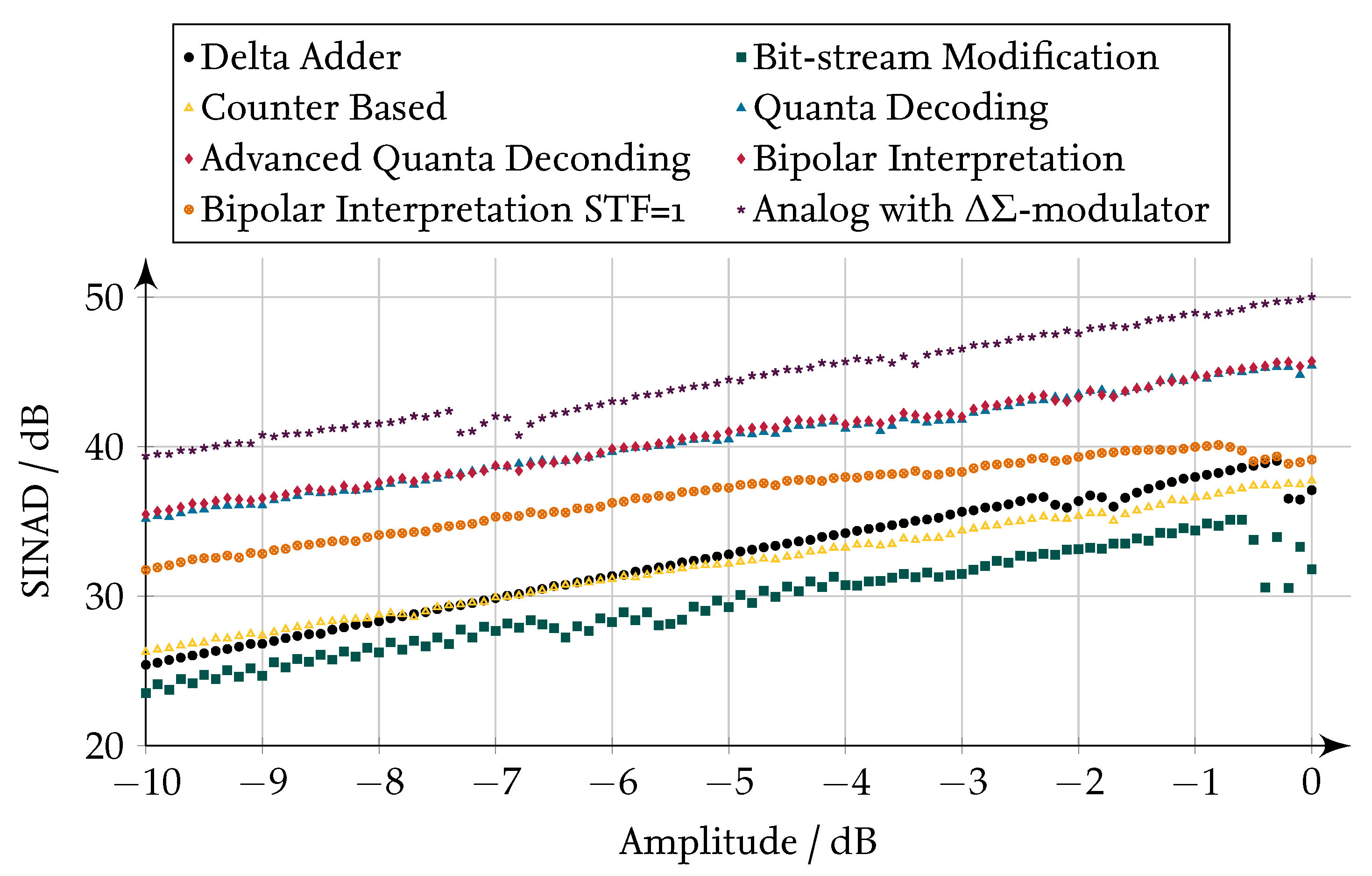
The presented SP implementations are compared with the test bench described in the previous subsection based on the algebraic operation addition. The two input signals are generated from a sinusoidal source scaled by 0.5 for one and 0.25 for the other input. The Sine wave has a fixed frequency of 128 and the -sampling frequency is 10 . To calculate the SINAD as measure of the signal quality, the spectra of the bit streams are calculated by means of brick wall filters with a decimation rate of 32. The results are shown in Figure 18.
The resulting SINAD of the second order Counter Based addition are omitted, since it is negative for all operation points. This behavior is expected, since second order -Ms require design and can not have uniform feedback paths [14,16]. Thus, only the first order Counter Based addition is discussed and referenced as Counter Based. As can be seen, the best result is achieved by an analog operation with a -M. Since, for all operations on the test bench in SP, two -Ms are utilized, one for the signal conversion of the multi-bit signal into a bit-stream and one internal as output stage, whereas, for DSP, only one -M as output stage is utilized, this result is expected. Thus, the multibit operation followed by a -modulator forms the upper limit for the achievable signal quality. On the other side of the scale the implementations Delta Adder, Bit-stream Modification and Counter Based achieve the lowest signal quality. This is also expected, as these implementations are based on internal first order -Ms resulting in a worse noise shaping for the quantization noise. The combination of different order -Ms in series has been discussed by [20]. The implementation Quanta Decoding reaches in average less SINAD than Advanced Quanta Decoding. If only one operation is in the signal path, this is negligible, but for cascaded operations, the noise accumulates significantly. The Bipolar Interpretation shows the same performance as the Advanced Quanta Decoding in this setting, as there is an even number of input signals and no previous scaling, thus both operation classes result in the same bit-stream and the signals quality is plotted only once. As the scaling of a single input can not be implemented by Advanced Quanta Decoding, the Bipolar Interpretation is rated as the best linear operation class, in consideration of the signal quality.
The second important measure is the introduced time delay. The evaluation, shown in Table 4, results in two groups. One group has nearly no delay with zero to one clock cycle and the other has nine clock cycles delay. The two implementations with nearly no delay, namely Delta Adder and Bit-stream Modification, have an internal first order -M. As stated in [11] the main delay time for Quanta Decoding, and therefore also for Bipolar Interpretation, depend on the utilized -M. In the simulations, the minimal parameter design from [16] is used. With another parameter design, from [15] for example, a signal transfer function without delay is possible (NTF = 1). The draw back of this solution is a reduction of the SINAD by averaged . Thus, the trade off between operation delay and signal quality can be tailored to the specific application. On the other hand, a delay of nine clock cycles at ≥10 is quite fast for systems usually controlled at ≤32 .
Another important measure is the resource demand, shown in Table 5. The implementations based on first order structures usually require less logic gates, than those based on second order structures. For example, the implementation Delta Adder only uses sxi logic cells, whereas the implementations for second order structures require 28–31 logic gates. The exception is Bit-stream Modification, which also requires 20 logic cells. This is due to the complex subtraction of as preparation step. Based on these results, the implementation costs does not favor any second order implementation class.
The operation integration, shown in Figure 19, needs particular attention. Since the actual integrator value, which is of type multibit, is added to the new input value, both values have to be offset free. Thus, the operation classes Delta Adder and Bit-stream Modification are not applicable. In general, the operation class Bit-stream Modification could be extended by subtracting 0.5 instead of 0.25. The disadvantage of this solution is that no negative numbers are representable. For the integration, a multibit limitation for the integrated value should be introduced to avoid an overdrive of the -M.
With the presented operation classes Quanta Decoding, Advanced Quanta Decoding and Bipolar Interpretation, all linear systems and controllers with bounded inputs, outputs and internal states can be described.
4. Nonlinear operations in Delta-Sigma Signal Processing
Nonlinear operations on bit-streams are a special topic to address. Due to the lack of an instantaneous value and the inherent noise shaping, some special precautions are required. For instance, a limitation of the represented value of the bit-stream cannot be implemented without averaging. Another problem occurs when two bit-streams are multiplied, as in the frequency domain this operation results in a convolution.
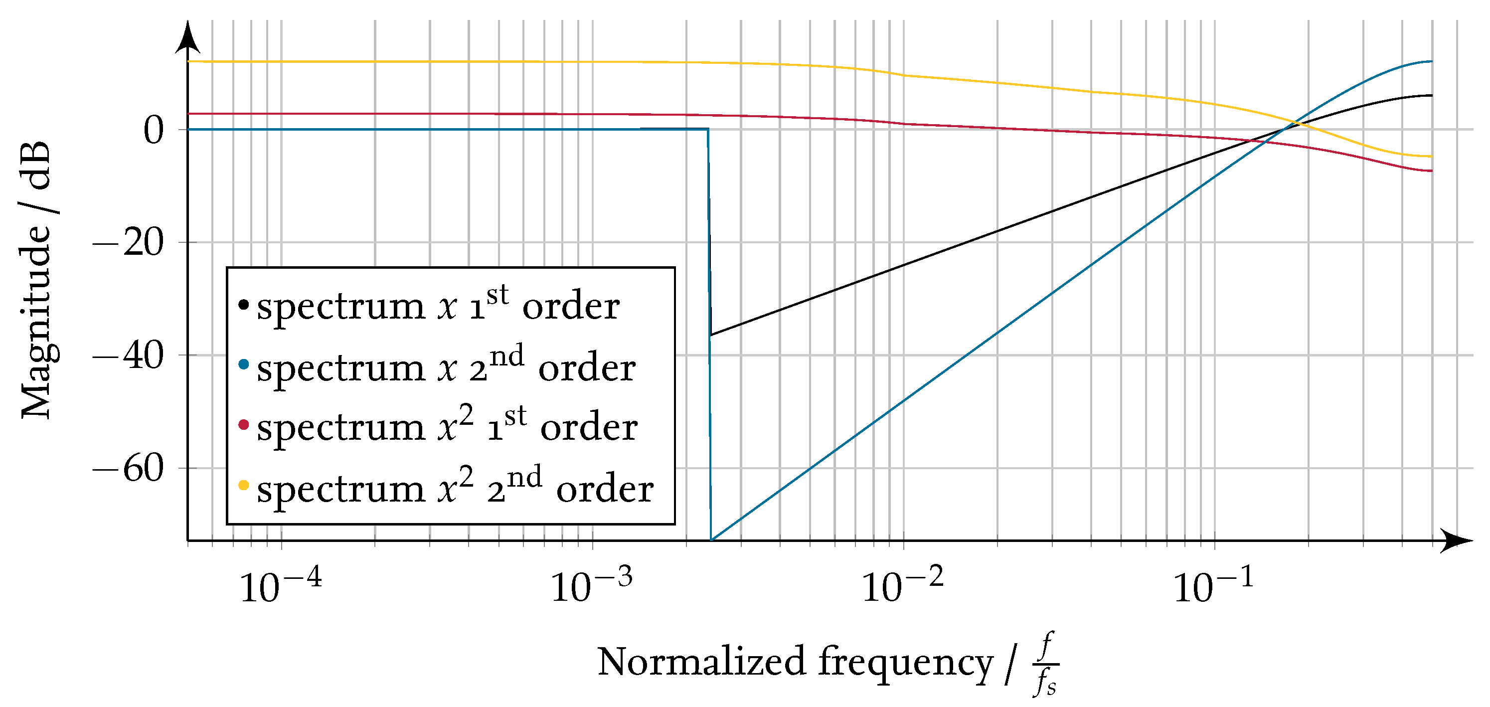
For illustrating the effects, the noise spectrum of a -M is superimposed with a fully loaded signal spectrum in the useful frequency band. This signal is chosen as an example because it has the most signal content possible. The resulting spectra for a first and a second order -Ms with an oversampling ratio of 32 are shown as spectrum in Figure 20. According to these spectra, possible signal sequences in the time domain are calculated by inverse fast Fourier transform. In this example, squaring is applied to the sequences, as a representative of the operation multiplication. In the last step, the spectra of the resulting sequences are evaluated by fast Fourier transform (spectrum squared in Figure 20). As can be seen, the noise in the squared signals is spread over the whole frequency domain. For the signal components a triangle with twice the width and the maximum amplitude of 0 is expected, as this results for the assumed signals without noise. The additional energy is spread noise folded down into the baseband by the multiplication. This results in a very poor possible signal quality, even with a low-pass filter for the baseband. In other words, the noise shaping is made ineffective by multiplication without further precautions.
4.1. Multiplication
In the field of control systems, the multiplication of two signals is a common algebraic operation. From the literature, there are different methods known for the multiplication of two bit-streams [17,28,29].
4.1.1. Based on Delta Adder
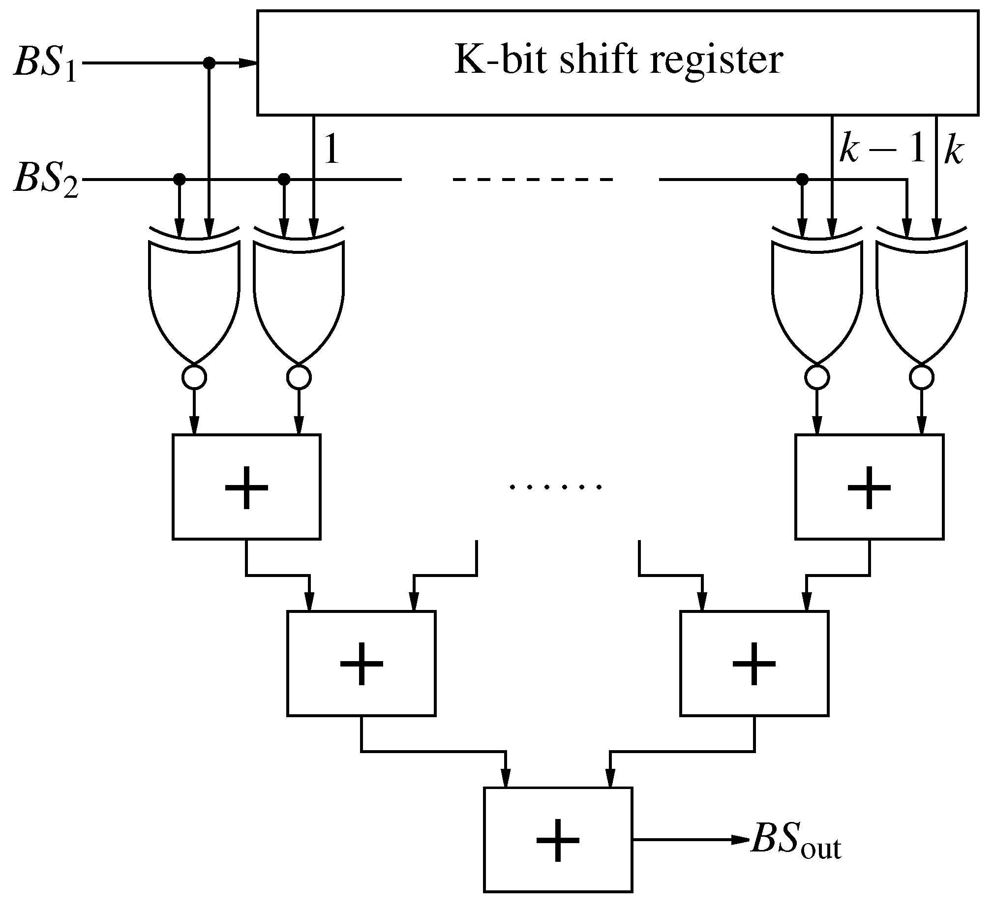
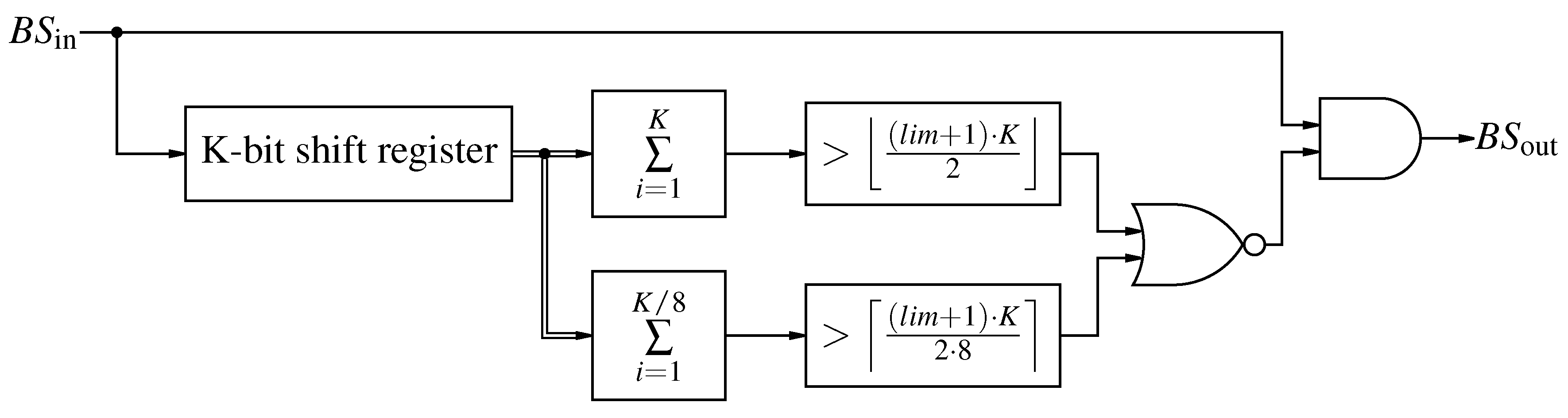
The first approaches are presented in [28]. The implementations utilize simple logic cells for a short filtering and the multiplication. As a drawback, the implementations request input bit-streams with scaled sampling frequencies (). The results show that a higher natural factor between the sampling rates leads to a higher signal to noise ratio. The multiplier was improved to process two bit-streams at the same input frequency, and is presented in [29]. The improved multiplier consists of a bit shift register for one bit-stream and multiplies each bin with the actual bit of the other bit-stream. The results are added via delta adder, as shown in Figure 21.
4.1.2. Based on Delta Adder Modified
Regarding the fact that the noise is shifted to the high frequency signal region and the k-bit shift register forms sort of a low-pass filter, it can be assumed that a second shift register for the other input achieves a further improvement in signal quality. The implementation with two shift registers is shown in Figure 22.
Due to the symmetry of the input bit-streams, the implementation can be simplified to the logic operation NOT, the logic operation XOR (XOR) and an averaging filter based on a shift register and Delta Adders, as shown in Figure 23. This implementation emphasizes the low-pass filter.
4.1.3. Based on Logic Operations
In [17], it is shown that logic operations can result in the multiplication of two signals. Especially the combination of the XOR and NOT are candidates for multiplying two bit-streams encoded in Bipolar Interpretation. The drawback of this solution is the necessity to statistically decouple the noise in the input bit-streams. This can be achieved by utilizing different designed -Ms. The independence of two bit-streams can be measured by the normed cross product without shift (Equation (13)), with zeros in bit-streams mapped to minus one.
The multiplication based on logic operations is shown in Figure 24. The previous approach based on Delta Adder can be transformed into this solution by using a shift register with the length 0.
4.1.4. Based on DSP
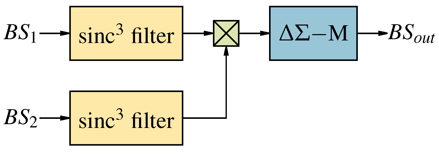
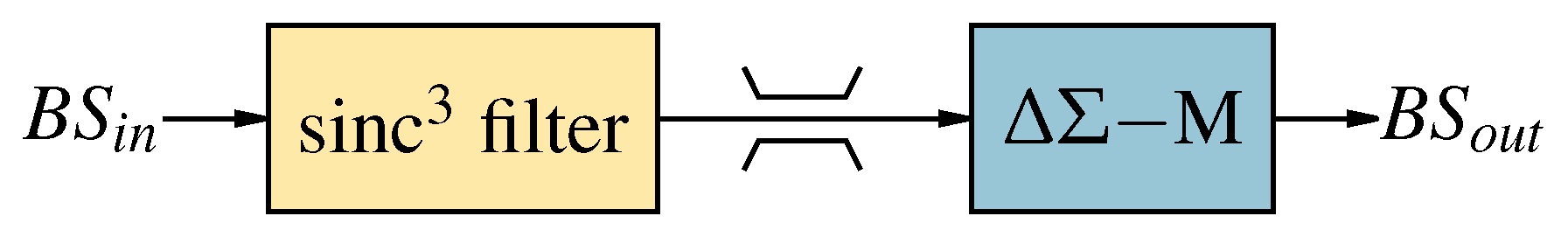
As the main problem for nonlinear functions is the lack of an instantaneous value, another approach is to utilize fast sinc filters with a small group delay in the range of the linear operation classes (see Table 4). As the multibit result of the arithmetic operation has to be modulated again, the group delay of the implemented -M adds to the group delay of the sinc filter. The basic implementation is shown in Figure 25. Similarly, for the linear operation class Bipolar Interpretation, the multiplication based on DSP is shown in Figure 26.
4.2. Limiting
Another important nonlinear algebraic operation in control systems is limiting. To limit the value of a bit-stream, the approximated instantaneous value has to be evaluated by averaging. The problem is, when the filtered value is valid, the output has already exceeded the intended limitation.
4.2.1. Based on Delay Taps
The problem of averaging can be addressed by a tapped averaging filter as a low-pass filter. Especially if different tap lengths are combined for accuracy and short response time. As shown in Figure 27, the last bits of the output bit-stream are stored and accumulated. For an upper limit, the sum is compared to the value representing the maximal output value (). If the sum exceeds the limit, a zero is output.
In the case of a lower limit, the sum is compared to the value representing the lower limit. If the sum falls below the limit, ones are output. The resulting schematic can be seen in Figure 28.
These operations can be cascaded to an upper and lower limit.
4.2.2. Based on DSP
4.3. Evaluation
As nonlinear functions change the frequency spectrum, the SINAD calculation is more complicated than for linear operations. To evaluate nonlinear functions, the focus is on the mapping quality and the delay. The mapping quality is measured via the variance and the delay with the step response, as known from linear operations. Only functions with one or two inputs are discussed in this paper, even though some can be extended to more inputs. For the measurement of the mapping quality, a sinusoidial source is connected to the first input and if the operation has a second input, a ramped signal is connected, as shown in Figure 30. For a function with two inputs, the step response is measured independently for each input with a constant value at the other input.
Results
All implementations are in fixed point, as they are targeted on a FPGA based platform. Since the results from simulation on a computer and operation on a FPGA do not differ, as they are both calculated digitally, the evaluated data are the result of simulations. The setup parameters are shown in Table 6. The setup time describes an additional simulation time in the beginning, which is not evaluated. The ramped input is constant for the setup time and the sinusoidal source is phase shifted to match a phase angle of 0 at the start of the recoding. The sinc filter length describes the count of samples processed in each sinc stage.
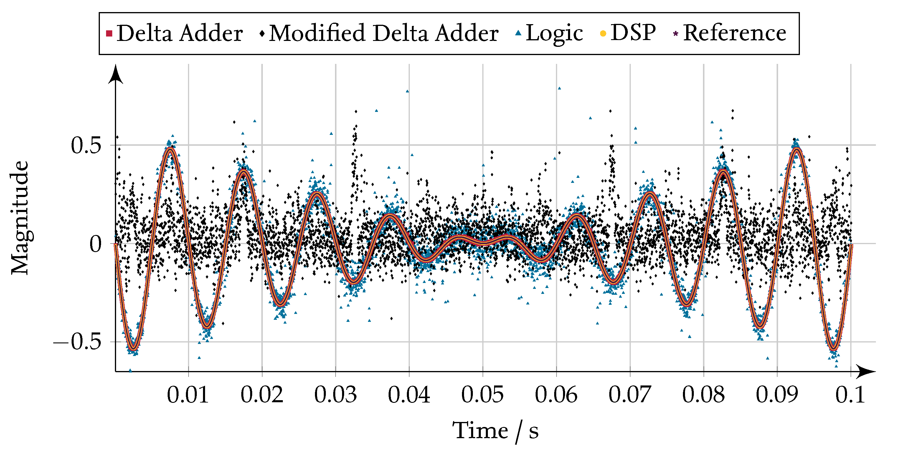
The signal processing runs at a sampling rate of 10 . Figure 31 shows the sinc filtered results for the different implementations of the multiplication. As can be seen, the modified Delta Adder based implementation produces mostly noise but not the expected signal. The resulting signal correlates only at maxima and minima with the expected signal, where in both cases, a positive peak can be obtained. The signal quality drops sharply, as the modified structure has an inherent disadvantage, namely the coupling of the input bit-streams, which is also a problem for inverted XOR logic based operations, as was already stated in [17]. Utilizing a second bit-shift register for the second input bit-stream, the same bit tuples will be shifted through the operation. This coupling leads to first the multiplication and afterwards the filtering. Thus, the noise shaping, as shown in Figure 20, is reversed. Therefore, the implementation with two bit-shift registers is discarded.
The mathematical metrics for the simulation of the multiplication are shown in Table 7 and the resource consumption on a FPGA are shown in Table 8. The implementation based on logic operations follows the desired output signal with some noise. The variance is three orders of magnitude larger than for the implementation based on Delta Adders or DSP. The great advantage is its short group delay. With six clock cycles it is twice as fast, as the DSP based implementation. The implementation based on Delta Adders comes close to this delay, if the average is taken. As stated in Table 9, the first input has a delay of 17 clock cycles and the second input has no delay at all. The implementation based on DSP results in the best variance. Thus, the optimal implementation for the operation multiplication depends on the requirements. If the highest priority is to save logic cells and signal quality is not important, the implementation based on logic operations is favored. If two signals are multiplied, of which at least one is changing slowly, the implementation based on Delta Adder can be advantageous, especially if no DSP blocks of the FPGA are available. If the signal quality has the highest priority or the delay for both signals should be the same, the implementation based on DSP is best suited.
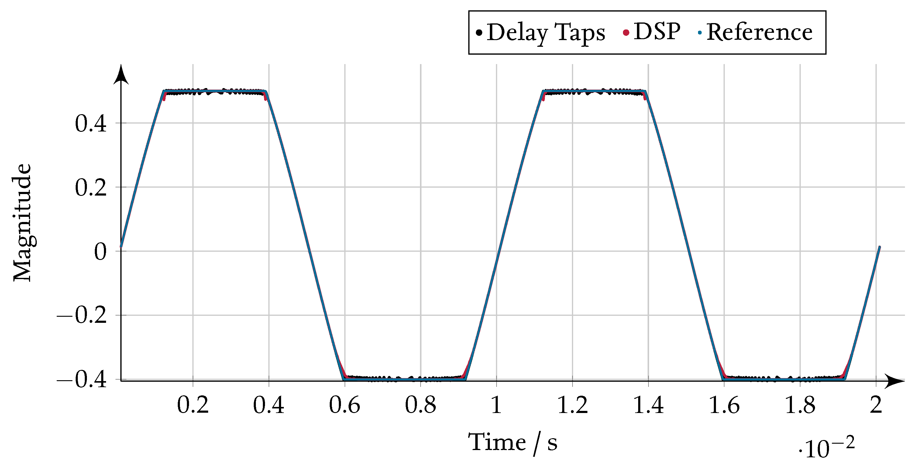
The sinc filtered results from the implementations for the operation limitation can be seen in Figure 32. If the input signal stays within the limit, the output signals track the reference signal. The implementation based on delay taps produces extra noise during saturation and thereby overshoots in some points. The variance of the DSP implemented limitation is caused by the deviations at the beginning and the end of the limiting. This results from the different filter length. The short and thereby fast sinc filter takes fewer bits into account for the actual value, thus the averaged value is already reaching the limit, whereby the longer filtered value stays below the limit. Because the average value is limited correctly, this effect only appears at entering and leaving of the limitation. The implementation based on delay taps has a shorter group delay than that based on DSP, with 1 in comparison to 15 clock cycles. In addition, the implementation based on delay tabs better tracks the limit, as shown in Table 9. Thus, the implementation with delay tabs is recommended as a general rule. The limitation based on DSP should be considered, if an adjacent operation to the limit is also implemented in DSP. In this case, no additional delay will be introduced, as the DSP operations can be combined, resulting in only one sinc filter and one -M. Another advantage of the implementation in DSP is shown in Table 10. The logic cell utilization of the DSP implementation is approximated 60% of the one based on delay taps as a stand alone operation. With an other adjacent operation based on DSP to the limitation the implementation cost can be reduced to eight logic cells, which scales with the signal width at the limiting.
5. Conclusions
Mathematical operations in the domain are divided into two classes: (1) linear operations; and (2) nonlinear operations. For linear operations, the implementations Delta Adders, Bit-stream Modification, Quanta Decoding, Advanced Quanta Decoding and Bipolar Interpretation have been discussed. As the results from the test bench show, all implementations based on second order -Ms result in a group delay of nine clock cycles. The best signal quality is achieved by the Bipolar Interpretation and the Advanced Quanta Decoding. Regarding the flexibility of the Bipolar Interpretation, to handle even and uneven counts of input bit-streams, this implementation class is recommended.
Nonlinear operations limit and multiply are discussed in this paper. The arithmetic operation multiply has been implemented based on Delta Adders, based on logic operations and in DSP. The latter shows the best signal quality. The resource cost is comparable to the implementation based on Delta Adders. The signal quality of the implementation based on logic operations is so low that it is suggested only if an estimation is sufficient. Thus, the implementation in DSP is suggested for the arithmetic operation multiplication.
The arithmetic operation limitation is evaluated for two implementations, one based on delay taps and the other based on DSP. Both implementations have their strength. Two advantages of implementation based on delay taps are the small group delay of one clock cycle and the better tracking in overflow, resulting in a lower variance. The DSP based implementation therefore always respects the limit and can be implemented by a relatively small number of logic cells, especially if an adjacent operation to the limit is also implemented in DSP.
In summary, DSP based operations are recommended for nonlinear arithmetic operations because they offer the greatest flexibility and can represent any nonlinear arithmetic operation. In some cases, special implementations provide better performance, such as the implementation based on delay taps for limitation. This advantage prevails at one single nonlinear arithmetic operation; at combination of several, the DSP comes into competition.
Author Contributions
A.K.: Conceptualization, Formal analysis, Investigation, Methodology, Software, Validation, Visualization, and Writing; and W.S.: Supervision and Writing.
Conflicts of Interest
The authors declare no conflict of interest.
Abbreviations
The following abbreviations are used in this manuscript:
| ADC | analog-to-digital converter |
| AND | logic operation AND |
| BS | bit-stream |
| DAC | digital-to-analog converter |
| ΔΣ | Delta-Sigma |
| ΔΣ-M | ΔΣ-modulator |
| DSP | digital signal processing |
| ΔΣSP | ΔΣ-signal processing |
| FA | full adder |
| FFT | fast Fourier transform |
| FPGA | field programmable gate array |
| LSB | least significant bit |
| MSB | most significant bit |
| NTF | noise transfer function |
| OR | logic operation OR |
| PWM | pulse width modulation |
| SINAD | signal-to-noise and distortion ratio |
| XOR | logic operation XOR |
| ZBS | “zero bit-stream” |
Symbols
The following symbols are used in this manuscript:
 |
 |
 |
 |
References
- Gröling, C. Optimierungspotenzial bei Servoumrichtern für permanenterregte Synchronmaschinen. Ph.D. Thesis, Technische Universität Braunschweig, Braunschweig, Germany, 2009. (In German). [Google Scholar]
- Homann, M.; Noeßelt, T.; Schumacher, W. Aspekte der Strommessung in Drehfeldmaschinen mit Delta Sigma Umsetzern. Available online: https://www.tib.eu/de/suchen/id/tema%3ATEMA20140600662/Aspekte-der-Strommessung-in-Drehfeldmaschinen-mit/ (accessed on 3 September 2018). (In German).
- Li, W.; Orino, Y.; Kurosawa, M.K.; Katagiri, T. Conversion of a single-bit signal into a PWM signal. In Proceedings of the 2004 IEEE Region 10 Conference, Chiang Mai, Thailand, 24 November 2004; pp. 519–522. [Google Scholar]
- Bradshaw, J.B. Bit-Stream Control of Doubly Fed Induction Generators. Ph.D. Thesis, University of Auckland, Auckland, New Zealand, 2012. [Google Scholar]
- Homann, M. Hochdynamische Strom-und Spannungsregelung von permanenterregten Synchronmaschinen auf Basis von Delta-Sigma Bitströmen. Ph.D. Thesis, Technische Universität Braunschweig, Braunschweig, Germany, 2016. (In German). [Google Scholar]
- Luckjiff, G.A. Sigma Delta Modulators with Hexagonal Quantisation. Ph.D. Thesis, University of Wisconsin-Madison, Madison, WI, USA, 2003. [Google Scholar]
- Schumacher, W.; Homann, M. Stromrichter und Computerprogramm. Available online: https://patents.google.com/patent/WO2015193439A1 (accessed on 3 September 2018). (In German).
- Homann, M.; Schumacher, W. High Bandwidth Phase Voltage and Phase Current Control Loop of a Permanent Magnet Synchronous Motor based on Delta Sigma Bitstreams. In Proceedings of the 18th European Conference on Power Electronics and Applications, Karlsruhe, Germany, 6 September 2016. [Google Scholar]
- Eynde, F.O.; Sansen, W. Analog Interfaces for Digital Signal Processing Systems; Springer: Boston, MA, USA, 1993. [Google Scholar]
- Aziz, P.M.; Sorensen, H.V.; Van der Spiegel, J. An overview of sigma-delta converters. IEEE Signal Process. Mag. 1996, 13, 61–84. [Google Scholar] [CrossRef]
- Homann, M.; Klein, A.; Kirchner, R.; Schumacher, W. Quasi-kontinuierliche Signalverarbeitung mit Delta Sigma Bitströmen in der Antriebstechnik—Ein Überblick. In Proceedings of the Fortschritte in der Antriebs-und Automatisierungstechnik, Stuttgart, Germany, 27 April 2016; pp. 215–227. [Google Scholar]
- Homann, M.; Klein, A.; Schumacher, W. Direct Delta Sigma Signal Processing for Control of Power Electronics. In Proceedings of the International Exhibition and Conference for Power Electronics, Intelligent Motion, Renewable Energy and Energy Management, Nuremberg, Germany, 10–12 May 2016. [Google Scholar]
- Kershaw, S.M.; Sandler, M.B. Digital signal processing on a sigma-delta bitstream. Available online: https://ieeexplore.ieee.org/stamp/stamp.jsp?tp=&arnumber=297578 (accessed on 3 September 2018).
- Schreier, R.; Temes, G.C. Understanding Delta-Sigma Data Converters; IEEE Press: Piscataway, NJ, USA, 2005. [Google Scholar]
- Schreier, R. Delta Sigma Toolbox. Available online: http://www.mathworks.com/matlabcentral/fileexchange/19-delta-sigma-toolbox (accessed on 3 September 2018).
- Marques, A.; Peluso, V.; Steyaert, M.S.; Sansen, W.M. Optimal parameters for ΔΣ modulator topologies. IEEE Trans. Circuits Syst. II Analog Digit. Signal Process. 1998, 45, 1232–1241. [Google Scholar] [CrossRef]
- Klein, A. Logic Operators on Delta-Sigma Bit-Streams. Math. Comput. Appl. 2018, 23, 4. [Google Scholar] [CrossRef]
- Kouvaras, N. Operations on delta-modulated signals and their application in the realization of digital filters. Radio Electron. Eng. 1978, 48, 431–438. [Google Scholar] [CrossRef]
- Fujisaka, H.; Kamio, T.; Ahn, C.J.; Haeiwa, K. Sequence characteristics of multi-level and second-order sigma-delta modulated signals. Nonlinear Theory Appl. IEICE 2013, 4, 313–339. [Google Scholar] [CrossRef] [Green Version]
- Liu, Y.; Furth, P.M.; Tang, W. Hardware-Efficient Delta Sigma-Based Digital Signal Processing Circuits for the Internet-of-Things. J. Low Power Electron. Appl. 2015, 5, 234. [Google Scholar] [CrossRef]
- Patel, N. Bit-Streams: Applications in Control. Ph.D. Thesis, University of Auckland, Auckland, New Zealand, 2006. [Google Scholar]
- Fujisaka, H.; Sakamoto, M.; Chang, J.A.; Kamio, T.; Haeiwa, K. Sorter-Based Arithmetic Circuits for Sigma-Delta Domain Signal Processing—Part II: Multiplication and Algebraic Functions. IEEE Trans. Circuits Syst. I Regul. Pap. 2012, 59, 1966–1979. [Google Scholar] [CrossRef]
- Cai, X.; Brooke, M. A compact CPU architecture for sensor signal processing. In Proceedings of the IEEE International Symposium on Circuits and Systems, Island of Kos, Greece, 21–24 May 2006; pp. 45–48. [Google Scholar]
- Pneumatikakis, A.; Deliyannis, T. Direct processing of sigma-delta signals. In Proceedings of the Third IEEE International Conference on Electronics, Circuits, and Systems, Rodos, Greece, 16 October 1996; Volumn 1, pp. 13–16. [Google Scholar]
- Patel, N.; Coghill, G.; Sing, K.N. Digital realization of analogue computing elements using bit streams. In Proceedings of the 3rd IEEE International Workshop on System-on-Chip for Real-Time Applications, Calgary, AB, Canada, 2 July 2003; pp. 76–80. [Google Scholar]
- O’Leary, P.; Maloberti, F. Bit stream adder for oversampling coded data. Electron. Lett. 1990, 26, 1708–1709. [Google Scholar] [CrossRef]
- Kester, W. Understand SINAD, ENOB, SNR, THD, THD + N, and SFDR so you don’t get lost in the noise floor. Available online: http://www.analog.com/media/en/training-seminars/tutorials/MT-003.pdf (accessed on 3 September 2018).
- Lagoyannis, D.; Pekmestzi, K. Multipliers of delta-sigma sequences. Radio Electron. Eng. 1981, 51, 281–286. [Google Scholar] [CrossRef]
- Lagoyannis, D.; Georgoudis, E.C. Multiplier of delta-sigma sequences of the same clock frequency. Int. J. Electron. 1984, 57, 423–427. [Google Scholar] [CrossRef]
Figure 1.
-M with lowpass filter in gray.

Figure 2.
Utilized second order -M as proposed in [16].
Figure 2.
Utilized second order -M as proposed in [16].
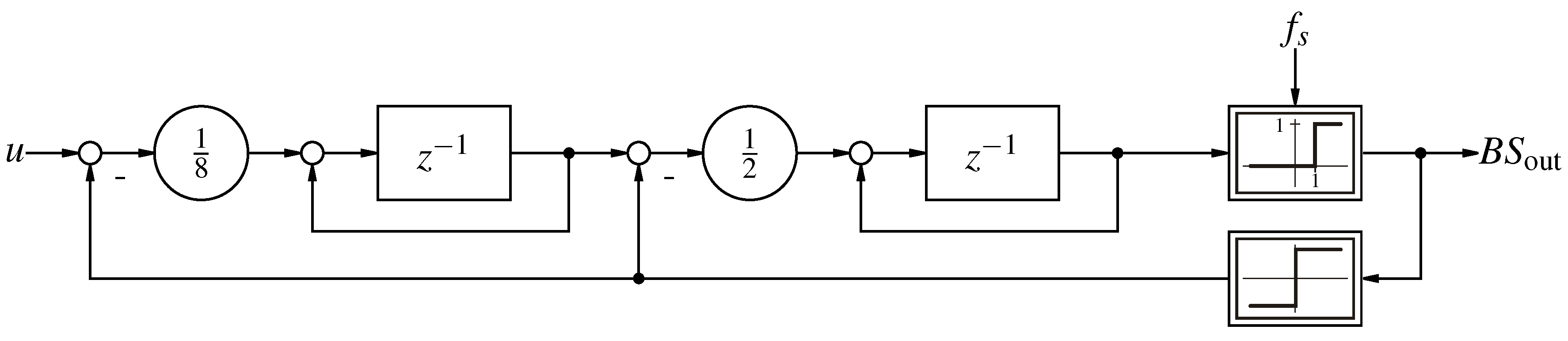
Figure 3.
Magnitude of the signal transfer function (STF) and noise transfer function (NTF) of a first order and a second order -M [11] over the frequency related to the sampling frequency ().
Figure 3.
Magnitude of the signal transfer function (STF) and noise transfer function (NTF) of a first order and a second order -M [11] over the frequency related to the sampling frequency ().

Figure 4.
Basic principle of a ΔΣSP operation with three internal steps and the equivalent DSP operation.
Figure 4.
Basic principle of a ΔΣSP operation with three internal steps and the equivalent DSP operation.

Figure 5.
Delta Adder in classical implementation [18] and its corresponding symbol.
Figure 5.
Delta Adder in classical implementation [18] and its corresponding symbol.

Figure 6.
Equivalent control scheme for Delta Adder [11].
Figure 6.
Equivalent control scheme for Delta Adder [11].

Figure 7.
Scaling based on Delta Adder, where is the ith bit from the MSB [18].
Figure 7.
Scaling based on Delta Adder, where is the ith bit from the MSB [18].

Figure 8.
Addition of two bit-streams using bit-stream modification with detailed description of the block .
Figure 8.
Addition of two bit-streams using bit-stream modification with detailed description of the block .

Figure 9.
Control system for adding a fixed value to a bit-stream.

Figure 10.
First order Counter Based addition of two bit-streams.

Figure 11.
Second order Counter Based addition of two bit-streams.

Figure 12.
Zero bit-stream generator based on a first order -M and a simplified implementation.

Figure 13.
The SP operation addition performed with Quanta Decoding.

Figure 14.
The SP operation addition performed with Advanced Quanta Decoding.

Figure 15.
Fundamental algebraic operation Bipolar Interpretation.

Figure 16.
The SP operation addition operated with Bipolar Interpretation.

Figure 17.
Test bench for evaluating linear SP.

Figure 18.
Resulting SINAD after the linear operation add with different SP implementations for a sine wave excitation with different magnitudes.
Figure 18.
Resulting SINAD after the linear operation add with different SP implementations for a sine wave excitation with different magnitudes.

Figure 19.
Generalized linear operation integration in SP.

Figure 20.
Output spectra of a first and a second order -Ms and of the signals squared in time domain.
Figure 20.
Output spectra of a first and a second order -Ms and of the signals squared in time domain.

Figure 21.
Multiplication of two bit-streams based on Delta Adder [29].
Figure 21.
Multiplication of two bit-streams based on Delta Adder [29].

Figure 22.
Modified multiplication of two bit-streams based on Delta Adder.
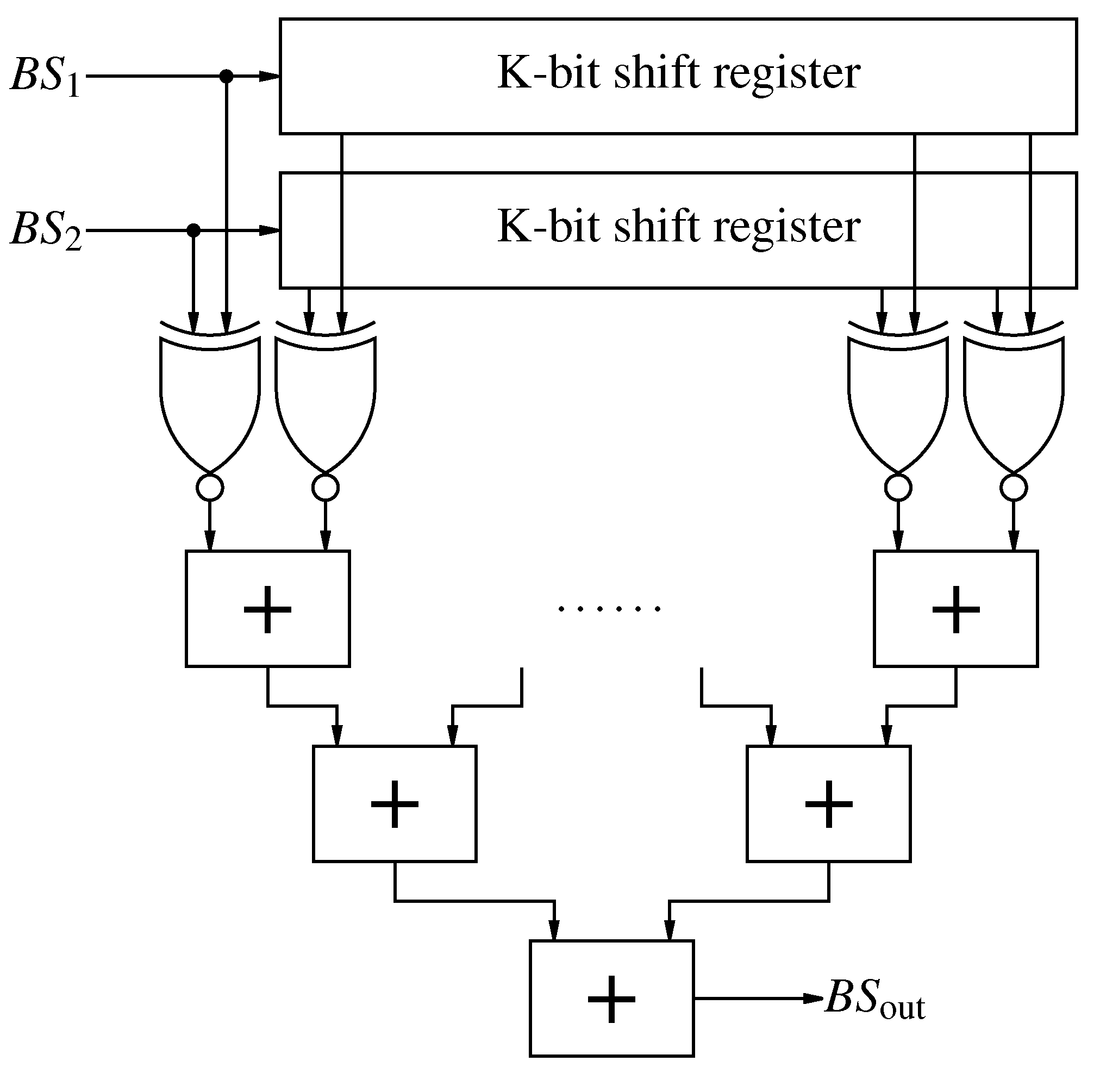
Figure 23.
Modified multiplication of two bit-streams based on Delta Adder with simpler implementation.
Figure 23.
Modified multiplication of two bit-streams based on Delta Adder with simpler implementation.
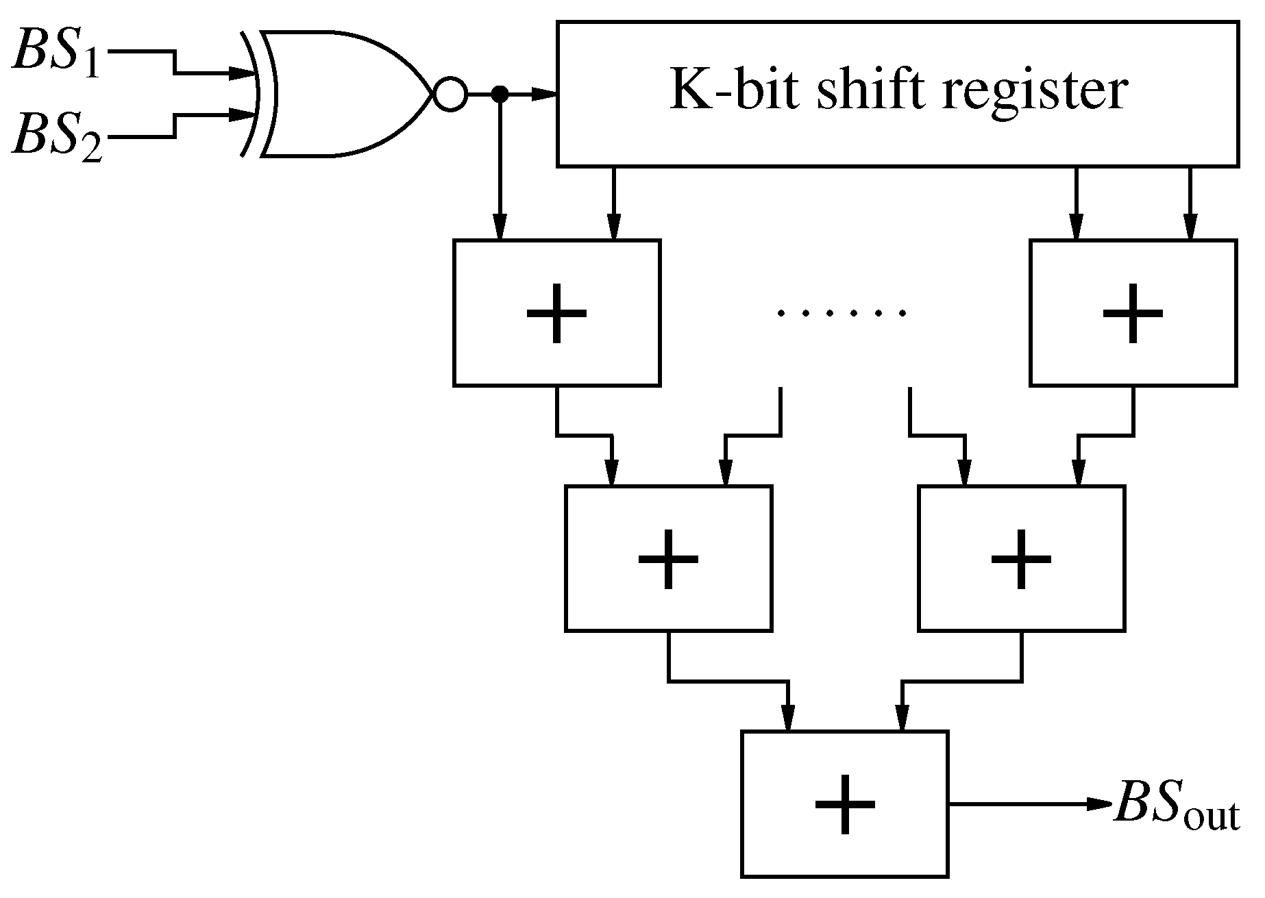
Figure 24.
Multiplication of two bit-streams using logic operations.

Figure 25.
Generalized nonlinear SP operation based an short sinc filters and DSP.

Figure 26.
Multiplication of two bit-streams using sinc filters and DSP operations.

Figure 27.
Limiting the upper value of a bit-stream using delay taps for averaging.

Figure 28.
Limiting the lower value of a bit-stream using delay taps for averaging.
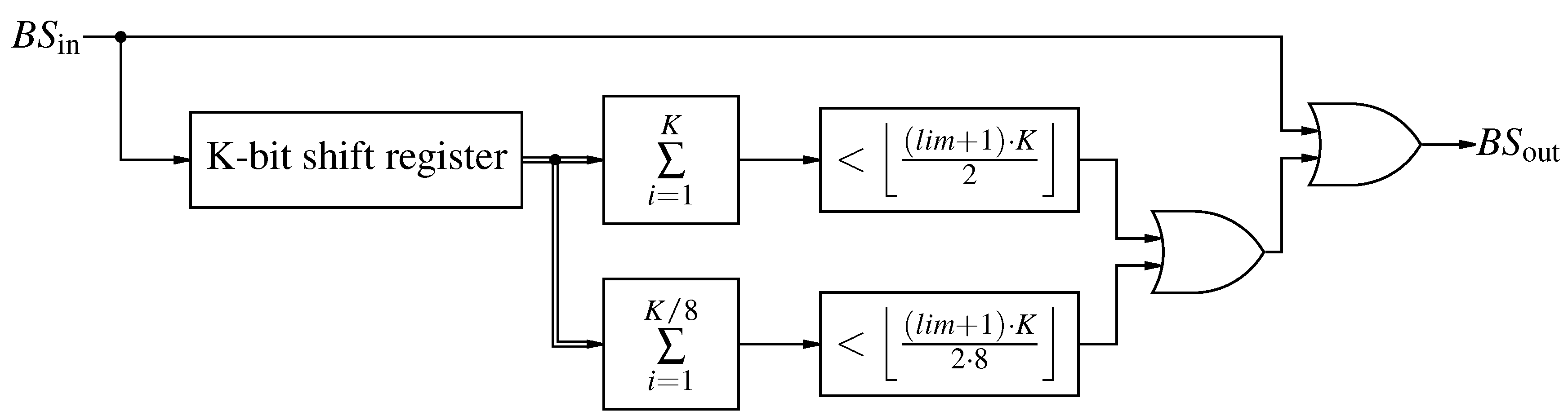
Figure 29.
Limiting the the value of a bit-stream utilizing DSP.

Figure 30.
Test bench for non linear functions with optional second input in gray.
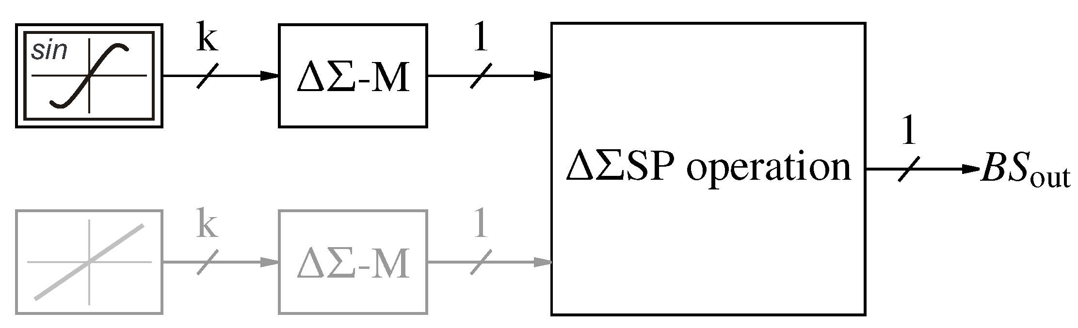
Figure 31.
Sinc filtered results for the multiplication with a decimation rate of 200.

Figure 32.
Sinc filtered results for the limitation with a decimation rate of 20.


Table 1.
Truth table of quantizer utilized by counter based operations.
| C | C | T |
|---|---|---|
| <0 | 0 | T |
| >0 | 1 | T |
| 0 | T | NOT(T) |
Table 2.
Truth table of a bit-stream (BS) minus the ZBS resulting in the quanta decoded value (QD).
| ZBS | BS | QD |
|---|---|---|
| 0 | 0 | 0 |
| 0 | 1 | +Q |
| 1 | 0 | −Q |
| 1 | 1 | 0 |
Table 3.
Logic table of two bit-streams (BS) and their “zero bit-streams” (ZBS), the quanta decoded value (QD) and the subtraction and addition of the quanta decoded values and direct operated bit-streams. In the highlighted rows, the “zero bit-streams” are equal.
Table 3.
Logic table of two bit-streams (BS) and their “zero bit-streams” (ZBS), the quanta decoded value (QD) and the subtraction and addition of the quanta decoded values and direct operated bit-streams. In the highlighted rows, the “zero bit-streams” are equal.
| ZBS | BS | ZBS | BS | QD | QD | − | + | ||
|---|---|---|---|---|---|---|---|---|---|
| 0 | 0 | 0 | 0 | 0 | 0 | 0 | 0 | 0 | 0 |
| 0 | 0 | 0 | 1 | 0 | 1 | −1 | −1 | 1 | 1 |
| 0 | 0 | 1 | 0 | 0 | −1 | 1 | 0 | −1 | 0 |
| 0 | 0 | 1 | 1 | 0 | 0 | 0 | −1 | 0 | 1 |
| 0 | 1 | 0 | 0 | 1 | 0 | 1 | 1 | 1 | 1 |
| 0 | 1 | 0 | 1 | 1 | 1 | 0 | 0 | 2 | 2 |
| 0 | 1 | 1 | 0 | 1 | −1 | 2 | 1 | 0 | 1 |
| 0 | 1 | 1 | 1 | 1 | 0 | 1 | 0 | 1 | 2 |
| 1 | 0 | 0 | 0 | −1 | 0 | −1 | 0 | −1 | 0 |
| 1 | 0 | 0 | 1 | −1 | 1 | −2 | −1 | 0 | 1 |
| 1 | 0 | 1 | 0 | −1 | −1 | 0 | 0 | −2 | 0 |
| 1 | 0 | 1 | 1 | −1 | 0 | −1 | −1 | −1 | 1 |
| 1 | 1 | 0 | 0 | 0 | 0 | 0 | 1 | 0 | 1 |
| 1 | 1 | 0 | 1 | 0 | 1 | −1 | 0 | 1 | 2 |
| 1 | 1 | 1 | 0 | 0 | −1 | 1 | 1 | −1 | 1 |
| 1 | 1 | 1 | 1 | 0 | 0 | 0 | 0 | 0 | 2 |
Table 4.
Phase delay in clock cycles of linear operation classes.
| Operation Class | Delay |
|---|---|
| Delta Adder | 0 |
| Bit-stream Modification | 1 |
| Quanta Decoding | 9 |
| Advanced Quanta Decoding | 9 |
| Bipolar Interpretation | 9 |
| Bipolar Interpretation | 0 |
| Counter Based | 2 |
Table 5.
Resource consumption of the implementations for addition on a FPGA.
| Implementation | Logic Cells |
|---|---|
| Delta Adder | 6 |
| Bit-stream Modification | 29 |
| Quanta Decoding | 31 |
| Advanced Quanta Decoding | 28 |
| Bipolar Interpretation | 28 |
| Bipolar Interpretation | 31 |
| Counter Based | 17 |
Table 6.
Simulation parameters.
| Parameter | Value |
|---|---|
| Sampling frequency | 10 |
| Simulation time | 0.10 s |
| Setup time | 50 |
| Sinusoidal amplitude | 0.75 |
| Sinusoidal frequency | 100 |
| Ramp start value | −0.75 |
| Ramp slope | 15 s−1 |
| DSP sinc filter length | 4 |
| Evaluation sinc filter length | 128 |
Table 7.
Variance and delay of the arithmetic operation multiplication (second input, if different).
Table 7.
Variance and delay of the arithmetic operation multiplication (second input, if different).
| Implementation | Variance | Delay |
|---|---|---|
| Delta Adder | 5.2934 × 10⁻⁶ | 17 (0) |
| Logic Operations | 3.4792 × 10⁻³ | 6 |
| DSP | 1.8948 × 10⁻⁷ | 12 |
Table 8.
Resource consumption of the implementations for multiplying on a FPGA.
| Implementation | Logic Cells | Multiplier (9 × 9) |
|---|---|---|
| Delta Adder | 318 | 0 |
| Logic Operations | 2 | 0 |
| DSP | 243 | 1 |
Table 9.
Variance and delay of the arithmetic operation limiting.
| Implementation | Variance | Delay |
|---|---|---|
| Delay Taps | 8.7516 × 10⁻⁶ | 1 |
| DSP | 1.3405 × 10⁻⁵ | 15 |
Table 10.
Resource consumption of the implementations for limiting on a FPGA.
| Implementation | Logic cells |
|---|---|
| Delay Taps | 303 |
| DSP | 181 |
© 2018 by the authors. Licensee MDPI, Basel, Switzerland. This article is an open access article distributed under the terms and conditions of the Creative Commons Attribution (CC BY) license (http://creativecommons.org/licenses/by/4.0/).
Share and Cite
MDPI and ACS Style
Klein, A.; Schumacher, W. Algebraic Operations on Delta-Sigma Bit-Streams. Math. Comput. Appl. 2018, 23, 49. https://doi.org/10.3390/mca23030049
AMA Style
Klein A, Schumacher W. Algebraic Operations on Delta-Sigma Bit-Streams. Mathematical and Computational Applications. 2018; 23(3):49. https://doi.org/10.3390/mca23030049
Chicago/Turabian StyleKlein, Axel, and Walter Schumacher. 2018. "Algebraic Operations on Delta-Sigma Bit-Streams" Mathematical and Computational Applications 23, no. 3: 49. https://doi.org/10.3390/mca23030049