3. Microreactor-Assisted Solution Deposition (MASD)
MASD processes were first developed with the intent to de-couple the homogeneous particle formation and deposition from the molecular level heterogeneous surface reaction [
12]. The MASD system has the capability to selectively produce intermediate, short-life molecules that are essential for the heterogeneous surface reaction on substrates, while avoiding the homogeneous particle formation reaction. This capability provides a better control of film growth and enhances the conversion of reactants into desired products (thin films). Many compound semiconductor thin films, including CdS, ZnS, CdTe, Cu
xSe, CuInS
2, CuInSe
2 and ZnO, have been fabricated by MASD [
13,
14,
15,
16,
17].
The MASD process was used to fabricate the CuInS
2 film on glass substrates by Park
et al. [
16]. Copper indium disulfide (CuInS
2) is one of the most promising ternary chalcopyrite materials, as an absorber in thin film solar cells, due to its direct band gap value (1.3–1.5 eV) [
18,
19,
20]. For the deposition of the ternary CuInS
2 compound, indium solution was first coated on the temperature-controlled substrate to form an indium precursor layer, and subsequently, a homogeneous mixture of copper and sulfur precursor solution from a micromixer was delivered onto the indium precursor-coated substrate. As-deposited CuInS
2 film was annealed at 200 °C for 1h in a vacuum furnace to generate a dense, crystalline thin film. It was found that the control of the thiourea concentration is critical in obtaining a single-phase CuInS
2 film. The molar concentration of thiourea also affects the morphology of CuInS
2 film. Polycrystalline CuInSe
2 film was deposited using the MASD process by Kim
et al. [
17]. It was found that the crystallinity of the film was affected by the composition of indium. Their work demonstrated the feasibility of fabricating smooth CuInSe
2 films with a large grain size, which is promising in solar cell applications.
ZnO, a transparent, wide bandgap semiconductor material, is one of the most studied materials among various metal oxides, because of the wide variety of nanostructure shapes, easier crystal growth and earth abundance [
21,
22,
23].
McPeak
et al. implemented the chemical bath deposition using a micro-flow cell to fabricate well-aligned ZnO nanowire arrays [
24]. They employed the spatial resolution of the microreactor to allow direct correlation of nanowire properties to process conditions. The results reveal that the lengths of nanowire decreased along the length of the flow cell, due to the depletion of precursors, morphology change from pyramidal tops to flat tops and the transition of growth mechanism from two-dimensional nuclei to spiral growth, as shown in
Figure 3.
Figure 3.
Cross-sectional SEM images of ZnO nanowires prepared at flow rates of 0.72 mL/h (
top row); and 2.88 mL/h (
bottom row) with an equimolar inlet concentration of zinc nitrate and Hexamethylenetetramine (HMT) Dimensions in each panel present the position where images were taken downstream from the inlet. The scale bar applies to all image. Reproduced from [
24].
Han
et al. reported the deposition of biomimetic nanostructured ZnO films using the MASD process, exhibiting anti-reflection on textured pyramidal silicon surfaces [
25]. The pyramidal silicon substrate was prepared by a wet chemical etching process. Ag nanoparticles (Ag NPs) were separately synthesized in a solution-based process and deposited on the pyramidal silicon substrate as the seed layer for the uniform deposition of ZnO nanostructures. Ag NPs also provided the nucleation sites for the initial formation of ZnO nanostructures, leading to the well-aligned orientation of the nanostructures. ZnO nanorods with a length of 400 to 500 nm were densely grown onto the Ag NP-coated pyramidal silicon substrate. Dense and uniform nanostructures are attributed to the heterogeneous surface reaction that is available by controlling the residence time, reaction temperature and precursor concentration in the MASD process. The deposition rate of nanostructures was measured to be around 125 nm∙min
−1, which is highly efficient in comparison to the conventional hydrothermal reaction. The comparison of reflectance measurement reveals that the reflectance is significantly reduced as ZnO nanostructures are deposited onto the pyramidal silicon surface.
In the following section, investigations of CdS thin films prepared by the MASD system are discussed in detail to illustrate its underlying principles and benefits.
Cadmium sulfide (CdS) is an important II-VI semiconductor that is finding applications in thin film transistor, photodetector and thin film solar cells [
26,
27,
28]. CdS is being used to create the p/n junctions in Cu(In,Ga)Se
2 and CdTe thin film solar cells. Among various synthetic approaches, chemical bath deposition (CBD) is a commonly used technique for the fabrication of CdS film, due to its simple manufacturing and large area fabrication.
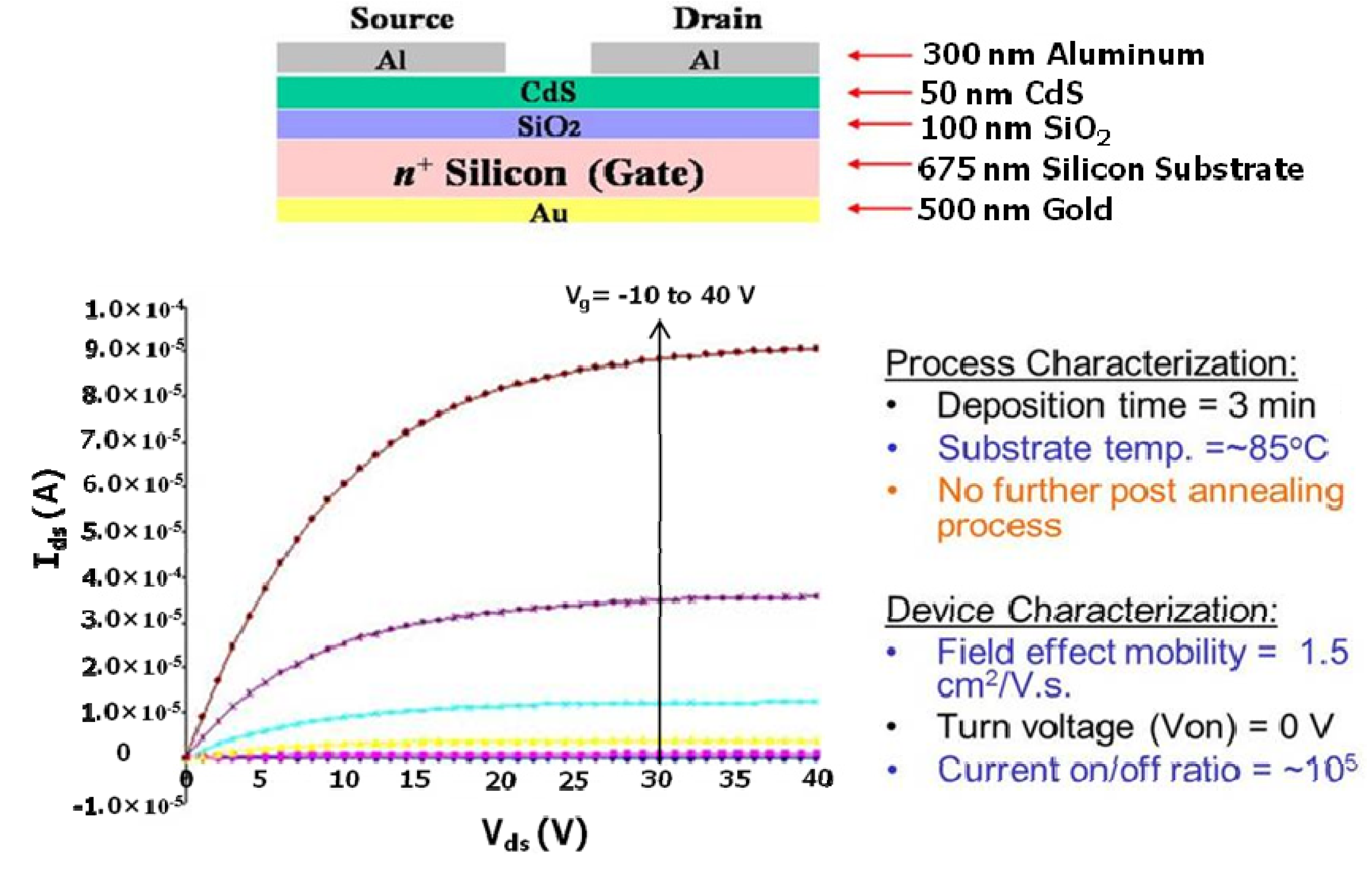
The MASD technique was first reported by Chang
et al. to deposit CdS thin film for the fabrication of thin film transistors at low temperature [
6,
12]. The reported MASD process, illustrated in
Figure 4, consisted of a micromixer, a digital pump, a heat exchanger and a hot plate. Solution 1 (a mixture of CdCl
2, NH
4Cl and NH
4OH) and Solution 2 (SC(NH
2)
2) are introduced into the mixing element and countercurrently enter the interdigital channels (30 µm), where they are spilt into many interpenetrated substreams. The substreams exit the interdigital channel perpendicular to the direction of the feed flows, initially with a multilayered structure. Rapid mixing through diffusion follows, due to the small thickness of the individual layer. The solution mixture of 1 and 2 pass a heat exchanger that supplies the constant reaction temperature and then are delivered onto the preheated substrate. This reactor provides the advantage of introducing constant flux of reactant solutions to the system (continuous process), which allows control over the homogeneous reaction of the chemical bath solution before the solution is delivered onto the substrate. This reactor successfully generated a reactant flux that is particle free by controlling the residence time. Using this particle-free flux, the authors were able to promote the molecule-by-molecule heterogeneous growth mechanism and prevent particle-by-particle growth [
6]. Enhancement-mode CdS metal insulator semiconductor field-effect transistors (MISFETs) (
Figure 5) was fabricated using this reactor at low temperature (80–90 °C) without any post-deposition annealing. An effective mobility, µ
eff ≈ 1.46 cm
2/V-sec, and a field-effect mobility, µ
FE ≈ 1.4 cm
2/V-sec, were obtained from this device [
12]. Arreola-Jardon
et al. reported that the as-deposited CdS-based thin film transistors fabricated from batch CBD show a field effect mobility in the range of 0.12–0.16 cm
2/V-sec [
27].
Figure 4.
Scheme of the microreactor-assisted solution deposition (MASD) technique for CdS film deposition. Reproduced from [
6].
Figure 4.
Scheme of the microreactor-assisted solution deposition (MASD) technique for CdS film deposition. Reproduced from [
6].
Figure 5.
Structure, device performance and output characteristic curves of CdS metal insulator semiconductor field-effect transistors (MISFETs). Reproduced from [
12].
Figure 5.
Structure, device performance and output characteristic curves of CdS metal insulator semiconductor field-effect transistors (MISFETs). Reproduced from [
12].
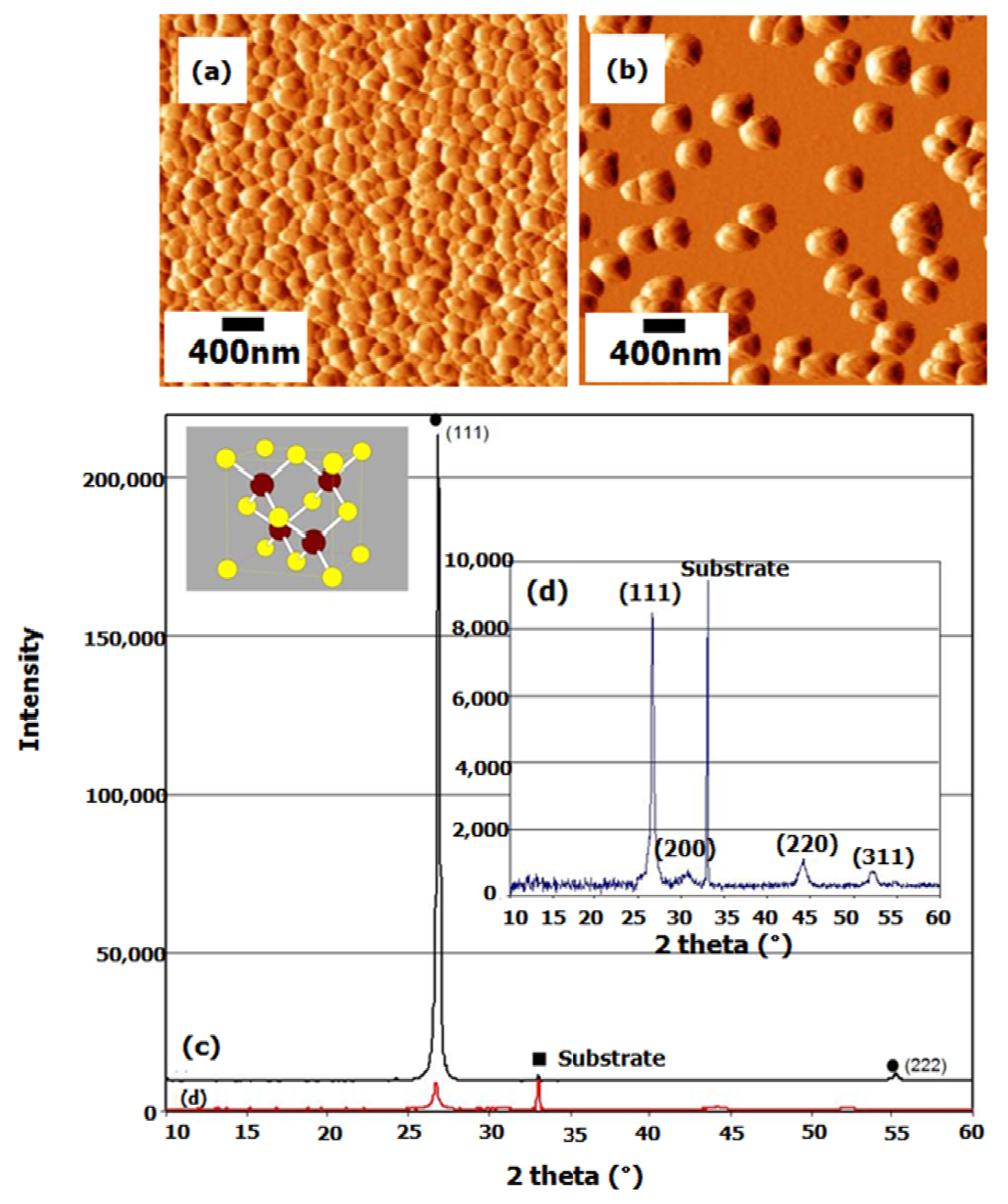
A comparison study of CdS thin film deposition by the MASD technique with the batch CBD was performed and reported by Mugdur
et al. [
29]. Having the same starting precursor concentration, reaction temperature and deposition time as the CBD, the CdS deposition by the MASD technique was carried out. AFM analysis of CdS film prepared by the MASD technique was compared with that prepared by the CBD (
Figure 6a,b). Dense and continuous film was obtained by the MASD technique, whereas discontinuous film was obtained by the CBD with the same deposition time. The RMS value of the roughness of the film by the MASD technique is 11.75 nm with a mean roughness of 9.61 nm. In contrast, the RMS value of film roughness by the batch CBD technique is 19.592 nm with a mean roughness of 15.795 nm. Two diffractogram peaks are shown in the XRD spectrum, corresponding to the (111) and (222) planes, respectively, from the cubic (zinc blends) phase (
Figure 6c). It is indicated that the film is strongly oriented along (111) with another small peak at (222) orientation. The presence of only (111) and (222) peaks indicates the highly oriented nature of CdS films deposited by MASD, which must grow as successive alternative planes composed of only either Cd or S atoms parallel to the substrate surface, as this corresponds to the (111) planes of the cubic crystalline structure. This type of growth is in good agreement with the molecular-level growth mechanism. In contrast,
Figure 6d shows a relatively broad XRD peak from the as-deposited CdS thin films by a batch CBD process that indicates its lower crystallinity.
Figure 7 shows a cross-sectional SEM image of a dense CdS thin film with a thickness of around 500 nm deposited by MASD. The terminal thickness of the batch CBD CdS is normally limited, due to the depletion of reactants. Thus, multiple depositions are required to deposit thicker and high quality CdS films by batch CBD. Previous results indicated that for CBD CdS deposition, small particles were forming and growing even at the beginning of the deposition process, as supported by real-time dynamic light scattering measurements and TEM characterization. We have observed a similar result using MASD (
Figure 8) [
6]. Experiments were carried out by pre-heating the precursor solutions (stream A and B) at 80 °C. At this temperature, thiourea releases more sulfide ions through hydrolysis. Free sulfide ions react with free cadmium ions to form CdS particles at these operation conditions. In order to obtain a solution without the homogeneous particle formation, the source chemicals have to be maintained at room temperature before they enter the micromixer. The mixed reactants are then maintained at 80 °C using heat exchanging fluid from a constant temperature circulator. TEM samples were obtained by collecting drops of hot solution from the Polyether ether ketone (PEEK) tube on the lacey carbon-coated TEM copper grid. TEM images (
Figure 8d) indicate that at very short residence times (e.g., 1 s), there was no evidence of particle formation on the surface of the grid under these processing conditions.
Figure 6.
Comparison study of CdS film grown by the MASD with CBD: AFM image of the film by (
a) the MASD and (
b) the CBD, respectively; the XRD spectrum of the film by (
c) the MASD and (
d) the CBD, respectively. Reproduced from [
29].
Figure 6.
Comparison study of CdS film grown by the MASD with CBD: AFM image of the film by (
a) the MASD and (
b) the CBD, respectively; the XRD spectrum of the film by (
c) the MASD and (
d) the CBD, respectively. Reproduced from [
29].
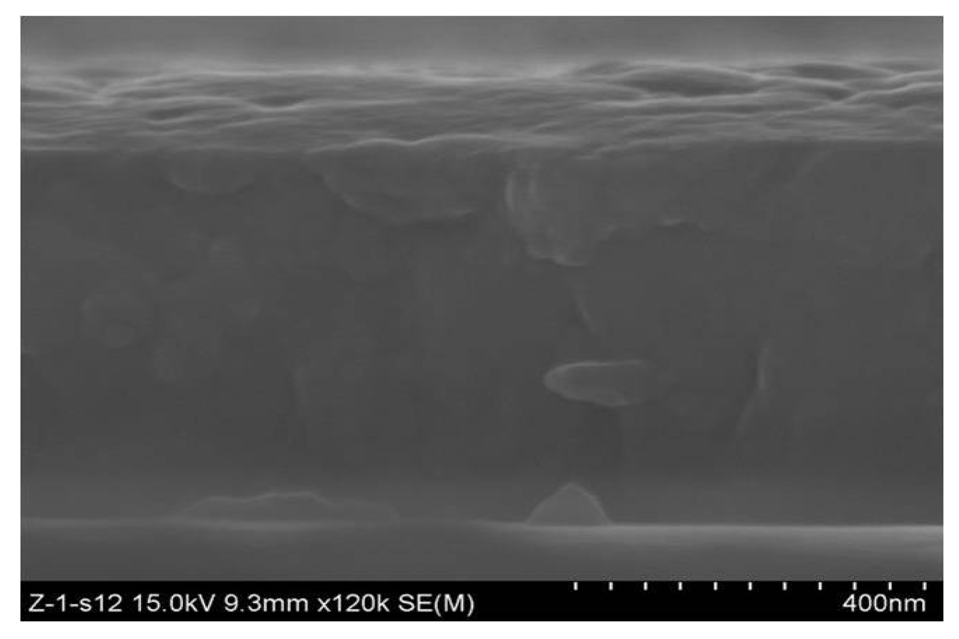
Figure 7.
Cross-sectional SEM image of the CdS film grown by the MASD.
Figure 7.
Cross-sectional SEM image of the CdS film grown by the MASD.
Figure 8.
TEM image of CdS nanoparticles generated from the continuous flow microreactor with a residence time of (
a) 1, (
b) 3.5 and (
c) 70 s by preheating the precursor solutions and with a residence time of (
d) 1 s for the precursor at room temperature. Reproduced from [
6].
Figure 8.
TEM image of CdS nanoparticles generated from the continuous flow microreactor with a residence time of (
a) 1, (
b) 3.5 and (
c) 70 s by preheating the precursor solutions and with a residence time of (
d) 1 s for the precursor at room temperature. Reproduced from [
6].
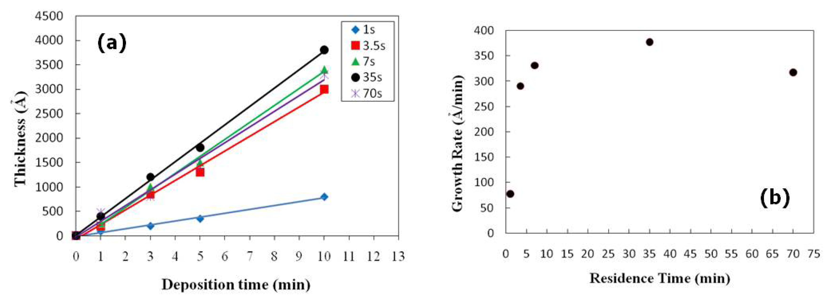
Using a particle-free flux study of the CdS deposition kinetics via the heterogeneous surface reaction by a molecule-by-molecule growth mechanism could be realized. A series of CdS thin film deposition experiments at different residence times (1, 3.5, 7, 35 and 70 s) were performed. The film thickness was determined by a surface profiler (Veeco, Plainview, NY, USA, 3D Dektak 8).
Figure 9a shows the deposited CdS thin film thickness
versus the deposition time at different residence times. The fitted linear regression lines were also plotted to obtain growth rate values. These growth rate results in
Figure 9b clearly indicate that a lower CdS thin film growth rate was obtained (~77 Ǻ/min) when a 1-s residence time was used. The growth rate increases significantly (about four times higher) when a 3.5-s residence time was used compared to a 1-s time. The thin film growth rate increases gradually from a 3.5-s to a 35-s residence time. However, when a 70-s residence time was used, the growth rate decreased. These results clearly demonstrate the capability of MASD to control the reaction kinetics of chemical solution deposition beyond the batch process. In addition, these results also demonstrate the utility of MASD as a valuable tool to investigate the chemical solution deposition processes. The pioneering studies by Ortega-Borges and Lincot and Doña and Herrero suggest that thiourea reacts with either cadmium hydroxide or dihydroxo-diammino-cadmium complex to form different adsorbed metastable complexes for CBD CdS deposition [
5,
30]. The proposed molecular-level heterogeneous reaction mechanism is given in Equations (1) to (3).
The CdS growth rates should be proportional to the concentration of thiourea, according to this reaction mechanism. The initial thiourea concentrations are the same for all of the MASD experiments. The thiourea concentration should decrease as a function of residence time, due to the hydrolysis Reaction 4:
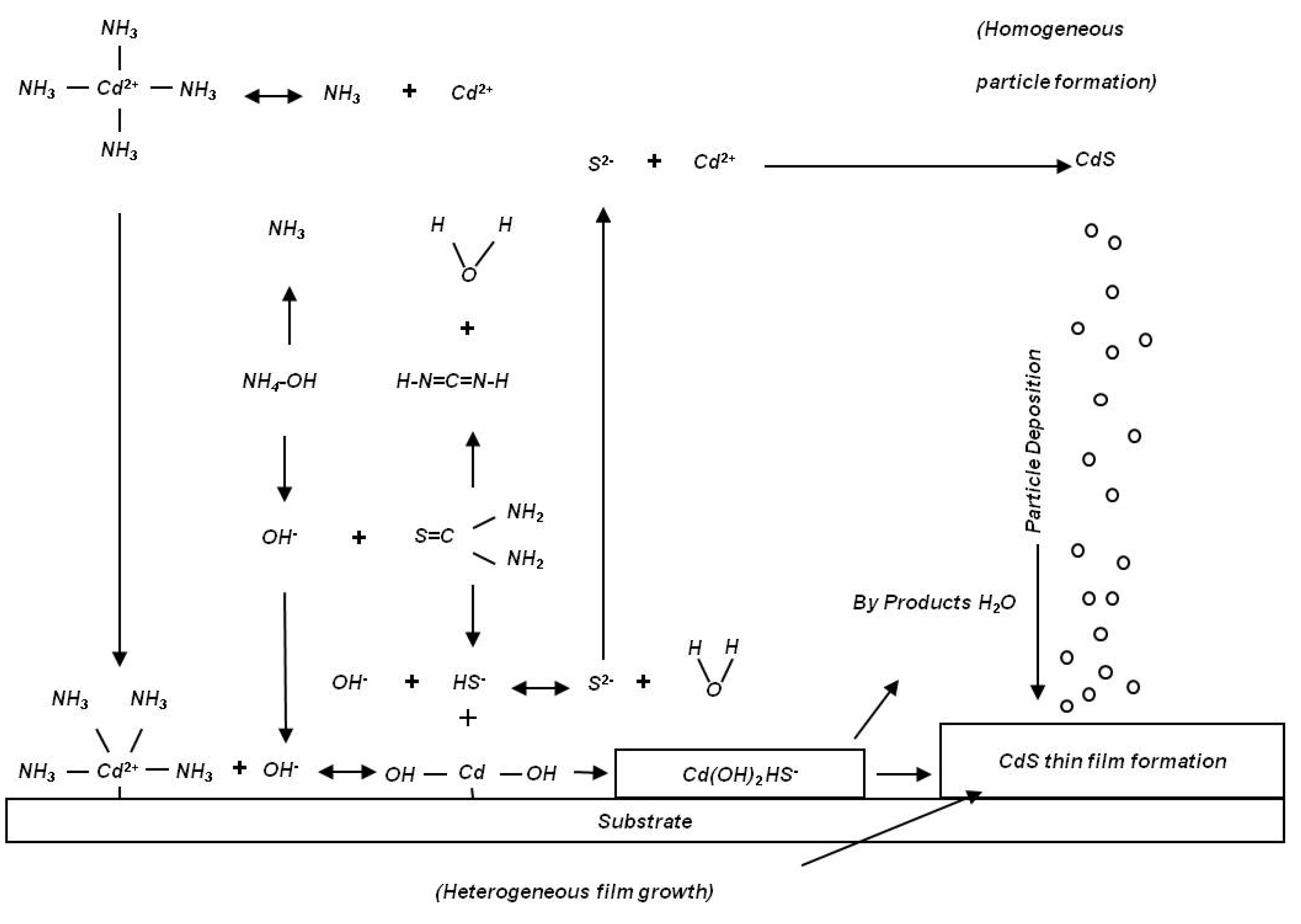
One would expect a slight reduction of the deposition rate at a longer residence time. The observed results suggest that the dominant reacting sulfur molecule that is responsible for CdS thin film deposition is not thiourea, but HS
−. At the short residence time of 1 s, the concentration of sulfide ions formed through the thiourea hydrolysis reactions and is lower than the concentration of sulfide ions at a longer residence time, thus resulting in a lower growth rate of CdS thin film. Between 35 and 70 s of residence time, nanoparticles start to form in the solution and to reduce the reacting molecular species. The proposed reaction mechanism is illustrated in
Figure 10 [
31].
Figure 9.
Fabrication of CdS thin film using MASD process: (
a) CdS thin film thickness
versus deposition time and (
b) growth rate as a function of different residence times. Reproduced from [
6].
Figure 9.
Fabrication of CdS thin film using MASD process: (
a) CdS thin film thickness
versus deposition time and (
b) growth rate as a function of different residence times. Reproduced from [
6].
Figure 10.
Growth mechanism of CdS thin film in the batch CBD process.
Figure 10.
Growth mechanism of CdS thin film in the batch CBD process.
In a conventional batch CBD process, the heat needed for chemical reaction is supplied from the solution bath to the sample surface, resulting in both heterogeneous CdS nucleation at the surface, as well as homogeneous CdS formation in the bath. Hence, for baths involving a thermal jacket (glass beaker,
etc.) or water bath, significant CdS deposition also occurs on the walls of the vessels. A significant amount of chemical precursors were converted into the formation of CdS particles in the solution. Normally, the bath was stirred continuously to ensure uniform thermal and chemical mixing and to minimize the sticking of CdS particles to the growing film surface. Moreover, the unequal volumes of the bath used to form the desired CdS film generates a lot of waste and creates defects in devices. Several groups of researchers have found ways to increase the precursor conversion yield [
32]. Boyle
et al. reported a modified CBD process that incorporate a filtration unit with the potential for continuous reaction by replenishment, treatment and purification of reagents within a recirculating closed-loop CBD reactor [
33]. Nair
et al. reported a technique to improve thin-film yield in the chemical bath deposition of semiconductor thin films [
32]. The concept is to use a very small substrate separation, 0.1 mm, to eliminate the passive layer of the bath, which contributes solely to precipitation. In small substrate separation, a thin layer of the bath mixture is held by surface tension between pairs of substrates. The thin-film yield obtained in their work approaches 100% for CuS, Cu
2−xSe, CdS and CdSe thin films. The final thickness estimated for the films is about 40–50 nm after a deposition time of 6 to 16 h. The combination of MASD with these innovative approaches should result in achieving an optimum film quality, growth rate and precursor by controlling the reacting chemical flux, the bath-to-surface volume and reaction temperatures.
4. Scale-Up of MASD Processes
To achieve reasonable volumetric flows, microchannel components are scaled-up by numbering-up
i.e., scaling-up by repeating microchannel unit operations in parallel to increase the cross-section of flow [
34,
35]. Numbering-up may be accomplished either internally or externally [
36]. Internal numbering-up involves arraying an original microchannel as an array of parallel microchannels within a single reactor component. An internal flow distribution system must be designed and implemented as part of the component to ensure equivalent reaction conditions in each channel. However, when scaling-up a process, the size of a single reactor component can be limited by either the size of the raw material available or the size of the work envelope for the fabrication processes used to produce the component [
35]. Consequently, external numbering-up can be used to scale-up the process further by putting a number of reactor components in parallel, allowing the original flow to be split evenly between the components. External numbering-up has the advantage that clogged components can be replaced without throwing away the remaining reaction capacity. However, external numbering-up can suffer from poor flow distribution between components and is logistically more difficult and expensive to implement.
Theoretically, the scale-up of microreactors is made easier by maintaining equivalent thermal, chemical and temporal reaction conditions within an array of microchannel unit operations. However, maintaining equivalent reaction conditions through channels of varying sizes and between components having different dimensions can be difficult, due to the effect on flow conditions. Saber
et al. investigated the effects of flow maldistribution on microreactor performance and found that for mass transfer-limited reactions, flow maldistribution had a more pronounced negative effect on reaction selectivity than for kinetic-limited reactions [
37]. Further, the researchers distinguished flow maldistribution due to poor manifolding during external numbering-up from that due to internal clogging. Internal clogging was found to have little effect on flow distribution, yet a relatively larger effect on the sensitivity of the reaction selectivity, due to reasons other than hydrodynamic effects. Tonomura
et al. performed numerical and experimental studies showing that pressure drop control is superior to total flow control for managing internal blockage between externally numbered-up components [
38]. The team validated these findings by implementing pressure drop control across four parallelized microchannel heat exchangers.
However, external numbering-up can be expensive, due to the amount of process control equipment required for each added device. Efforts have been made to simplify external numbering-up through the use of flow splitters that efficiently distribute a single flow into several uniform subflows, reducing the number of pumps [
36,
39]. Kashid
et al. demonstrated the external numbering-up of a two-phase capillary reactor using two six-channel polytetrafluoroethylene (PTFE) flow distributors (one for gas and one for liquid), six Y-shaped mixing elements and six glass capillaries [
40]. Though no reactions were conducted, the mass transfer characteristics for the six channel unit were found to track with those of a single capillary.
The technical literature provides various demonstrations for scaling the production of various chemistries using microchannel reactor technology. Iwasaki
et al. demonstrated six days of operation of a microchemical pilot plant consisting of a static T-micromixer followed by eight microtube reactors in a tube-and-shell arrangement for the numbering-up of a radical polymerization reaction [
41]. Results showed that at eight-fold the flow rate, a similar yield, molecular weight and molecular weight distribution were produced in the numbered-up reactor compared to the single microtube reactor. Deshmukh
et al. demonstrated the ability to scale-up the Fischer–Tropsch synthesis of synthetic fuels from a single microchannel to 276 parallel process microchannels at a production rate of 1.5 gallons per day [
42]. The process was found to provide equivalent outcomes, including syngas conversion and selectivity to a byproduct, across three orders of magnitude. Mae
et al. (2004) introduced two types of splitting and recombination micromixers that enabled the rapid aqueous extraction of phenol from dodecane within one second under a flow rate of 5–20 liters per hour [
43]. Kockmann
et al. demonstrated the numbering-up of a two-step organo-metallic reaction operated at two temperature levels [
44]. The final reactor contained 1 mm in diameter mixing channels and supported overall production rates of 700 grams per minute, leading to the production of more than two tons of isolated material. Bally
et al. discussed the design of a 2000 metric tons per year pilot plant with 28 interdigitated micromixers to mix the inlet flow of four tubular reactors to avoid precipitation in homogeneous polymerization reactions, which formed the basis of a patent [
45,
46]. Many additional examples of microreactor pilot plants for organic syntheses are provided by Wirth [
47]. Fox
et al. describe a numbered-up pulsed electric field reactor design for use in pasteurization [
48].
CBD is relatively easy to scale-up across large surfaces. However, as a batch process, CBD can offer low material utilization for chemistries involving competing reactions. MASD techniques are capable of providing the reaction selectivity and a short-life, intermediate chemistry unattainable in CBD. Other benefits include reduced energy requirements and processing times for long synthesis reactions and characteristically small reaction volumes, which can reduce human exposure to hazardous chemistries. The benefits of using microchannel reactors are primarily realized in diffusion-limited processes. An estimate for the mean time needed for molecules to diffuse in mass transfer is to the square of the channel radius over the diffusivity coefficient of the chemistry. Therefore, a tenfold reduction in tube diameter results in a one hundred-fold reduction in the residence time. The accelerated heat and mass transfer provides better process control, while reducing the size and weight of reactors. For diffusion-limited reactions, the use of microchannel components reduces the size and weight of the reactor apparatus, making implementation of MASD easier. Through the use of microchannel reactor components, temporal control of the chemistry enables the reactant stream to be introduced to the reaction surface at the peak of its reaction potential. Conceptually, a continuous flow MASD reactor for producing thin films from reactive chemistry will include a micromixer, a heat exchanger, a residence time unit and a flow cell for controlling deposition onto a substrate (see
Figure 11). A scale-up study of MASD using a flow cell was reported by Paul
et al. [
9,
49,
50].
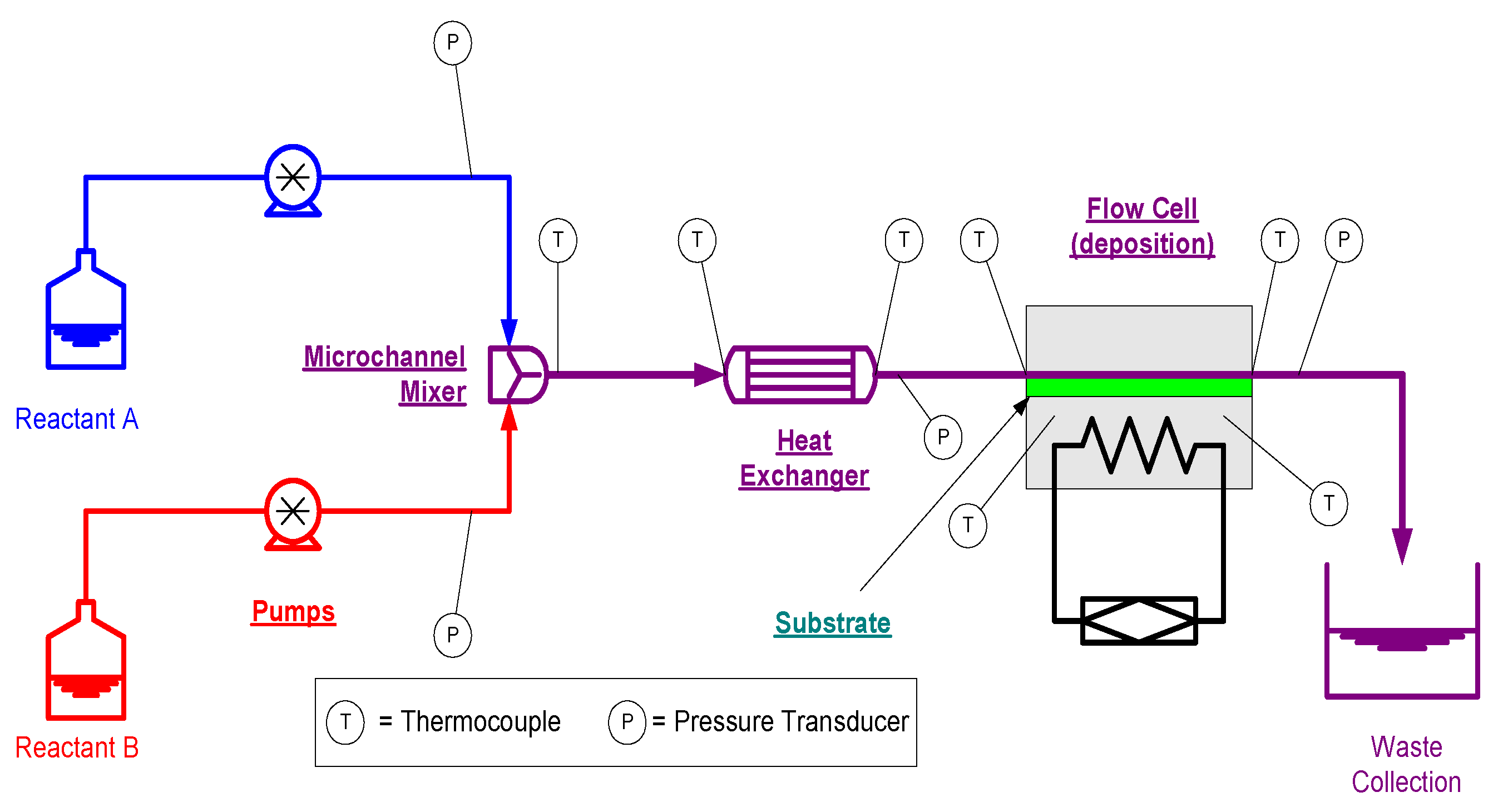
Figure 11.
A typical MASD setup. Reproduced from [
49].
Figure 11.
A typical MASD setup. Reproduced from [
49].
While the numbering-up of pilot plants have been demonstrated for many chemistries, a key to enabling MASD is the use of small, lightweight reactors capable of providing the distributed production of solution chemistries. The size and weight of microchannel reactors was envisioned early in the development of microreactor technology for enabling the distributed production of chemical products [
51]. A key component of MASD is a micromixer. Micromixers offer features that cannot be easily achieved by macroscopic devices, such as ultrafast mixing on the microscale. For example, Bökenkamp
et al. fabricated a micromixer as a quench-flow reactor to study fast reactions (millisecond time resolution) [
52]. A variety of micromixers have been reported in the literature, including static and dynamic mixers [
53,
54]. A simple T-mixer was used in the 6'' MASD system reported by Paul
et al. [
48]. T-mixers are relatively cheap and simple to fabricate; however, they might face a limitation to further scaling up. Other micromixers, such as oscillatory flow mixers and interdigital micromixers, could be used for the higher flow requirement. Oscillatory flow mixers fall into two categories. Pressure-driven oscillatory mixers have been shown to be capable of sustaining the largest production rates of nanoparticle chemistries reported to date, while piezo-driven ones, being compact and precise, have not been shown to provide adequate production rates [
55,
56]. Interdigital micromixers seem to provide the smallest format at a reasonable production volume. In the case of numbering-up the synthesis of phosphine-stabilized undecagold nanoclusters, Jin
et al. used an interdigital micromixer to demonstrate a production rate 500 times greater and a yield over 3.5 times higher than that of a conventional batch process [
57]. To demonstrate the ability to internally number-up the reaction, the number of plates in the mixer was doubled (double the flow cross-section) and the overall flow rate was quintupled, leading to a five-fold increase in the production rate to 7.1 kg per week, while maintaining a constant material conversion rate. The largest micromixer used was just under 1.7 cm
3 in volume.
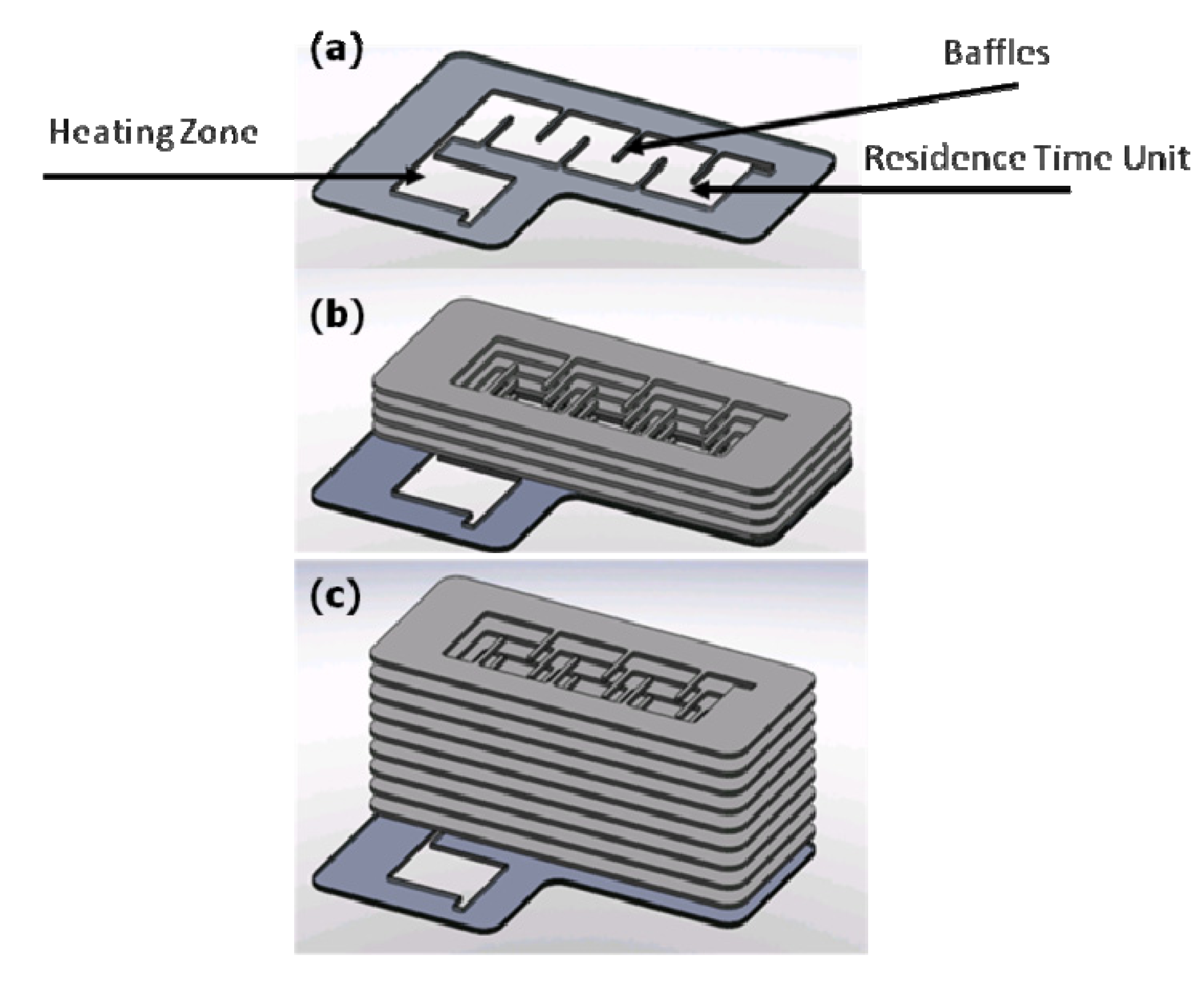
Ramprasad
et al. developed an adjustable residence time heat exchanger, suitable for MASD, comprised of two sections integrated in a single device; a rapid heating zone (HZ) and an adjustable residence time (RT) section, as shown in
Figure 12 [
9]. The heat exchanger is a composite unit consisting of copper plates at the top and bottom, to seal the polycarbonate channels, which are interposed between silicone gaskets. Copper was chosen because of its high thermal conductivity. An ESI (Portland, OR, USA) Laser 5330 was used for machining of the micro-channels in polycarbonate and silicone. This entire unit was bolted together to provide a leak-proof system. The HZ is the initial section of the polycarbonate channel in which the mixed reagents enter at room temperature and are heated to the set-point temperature in roughly one second. The hot fluid exiting from the heating zone enters the RT unit of the heat exchanger. The function of the RT unit is to maintain the fluid at the HZ exit temperature, while providing the specific additional residence time of the hot fluid before deposition onto the substrate (
Figure 13). The residence time in the heat exchanger is contingent on the number of polycarbonate plates in the heat exchanger assembly. The heat exchanger is designed such that the first polycarbonate plate is an integrated device consisting of both the HZ and the RT unit. This integrated unit of the HZ and RT polycarbonate plate is sandwiched between two silicone gaskets. However, the option of exclusively augmenting only the polycarbonate RT plates may be utilized to achieve the desired higher residence time. The schematic of the residence time configuration is shown in
Figure 11. Two silicone strip heaters are overlaid onto the RT units both on the top and bottom to provide sufficient heat to maintain the fluid at the desired temperature. A total of four ceramic heaters were used, with two heaters on each face of the HZ section.
Figure 12.
A schematic representation of residence time configurations available in the adjustable residence time heat exchanger (
a) 1×; (
b) 5×; (
c) 10×. Reproduced from [
9].
Figure 12.
A schematic representation of residence time configurations available in the adjustable residence time heat exchanger (
a) 1×; (
b) 5×; (
c) 10×. Reproduced from [
9].
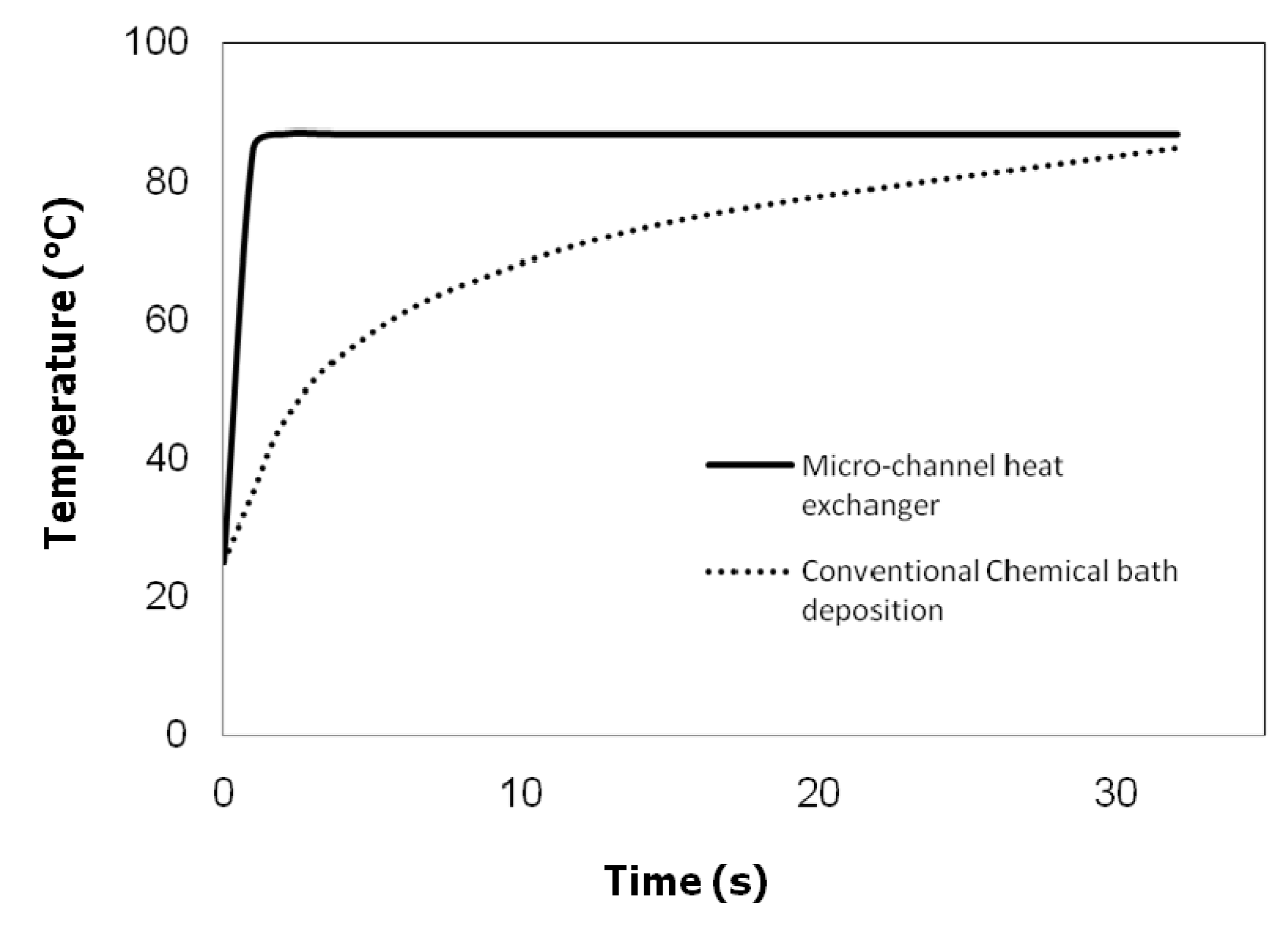
Figure 13.
The temperature variation as a function of the residence time in a comparison of a micro-channel heat exchanger with conventional chemical bath deposition. Reproduced from [
9].
Figure 13.
The temperature variation as a function of the residence time in a comparison of a micro-channel heat exchanger with conventional chemical bath deposition. Reproduced from [
9].
A key challenge for scaling up MASD is the requirement for film uniformity over large substrates, which requires that reaction conditions are uniform over the target substrate. Surface reaction kinetics are highly dependent on the reactant concentration and temperature at the reactive surface. In the case of reactants supplied as a continuously flowing fluid, the velocity at which the fluid travels determines the residence time over which the reactants have access to the deposition surface. For large substrates 150 mm-wide or more, it can be difficult to maintain constant fluid residence time across the entire surface. Further, faster flowing fluid results in a thinner boundary layer through which reactants diffuse. This difference in residence time and boundary layer thickness produces a variable film thickness, which is undesirable for the final cell functionality.
In a pressure gradient-driven system, a challenge arises when transforming a virtual “point source” fluid supply from tubing to a uniform velocity front across a comparatively large surface area and then back to tubing for collection. In this chapter, the function of a flow cell is to manage flow distribution across the thin film substrate. Little has been published regarding flow cell designs used in scaling up liquid-phase continuous flow deposition.
The basic flow cell design consists of a fluid cavity between two parallel plates with an inlet and an outlet. Efforts have been made in adjacent fields to manage flow distribution within various types of flow cell arrangements. Chung
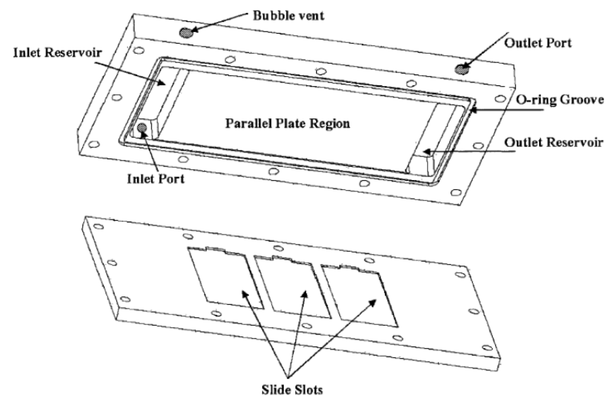
et al. presented a flow cell design for cell culture cultivation having over-sized inlet and outlet reservoirs designed as long plenums, as shown in
Figure 14 [
58]. The long plenums have a low pressure drop, which helps to distribute the fluid laterally prior to flowing over the parallel plate region, effectively managing the lateral variation of fluid velocity.
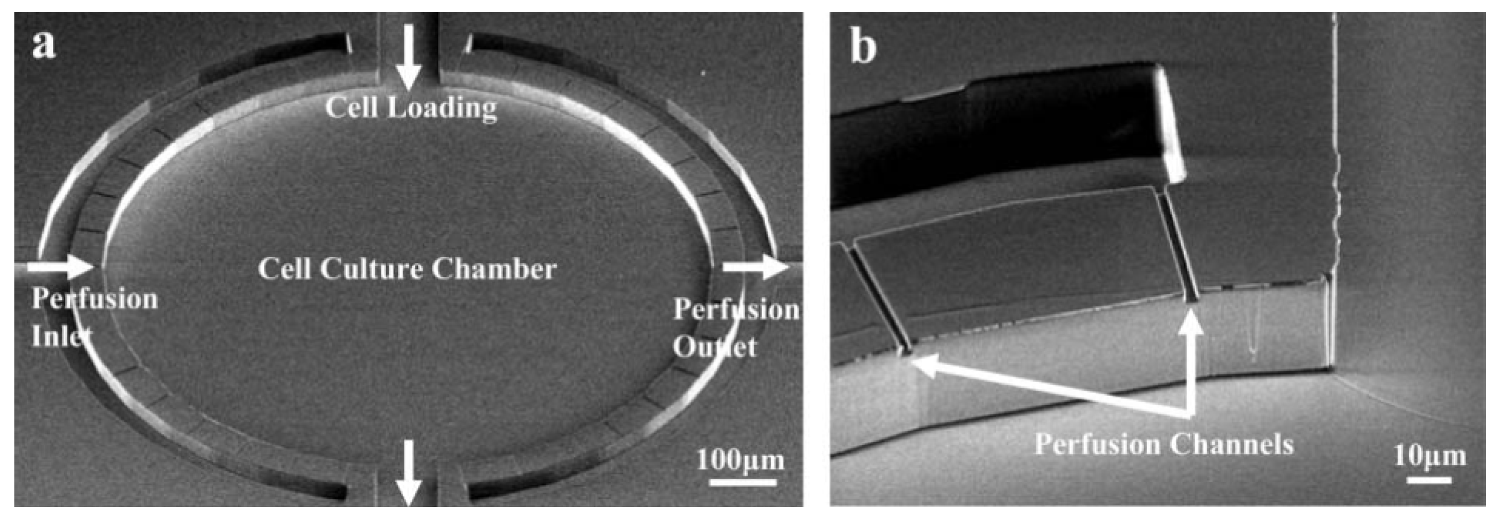
In a similar manner, PDMS flow cells were developed by Hung
et al. to provide nutrients to a cell culture system in a uniform and controlled manner [
59]. An outer plenum was connected to the flow cell using small perfusion channels, which have greatly reduced cross-sectional areas and much larger pressure drops than the plenum (
Figure 15). The size of the perfusion channels can be used to effectively manage the fluid velocity across the flow cell (
Figure 16).
Figure 14.
Schematic of flow chamber with inlet/outlet reservoirs. Reproduced from [
58].
Figure 14.
Schematic of flow chamber with inlet/outlet reservoirs. Reproduced from [
58].
Figure 15.
(
a) Magnified view of the cell chamber; (
b) magnified view of the perfusion channels. Reproduced from [
59].
Figure 15.
(
a) Magnified view of the cell chamber; (
b) magnified view of the perfusion channels. Reproduced from [
59].
Figure 16.
(
a) Time-stepped computational fluid dynamics (CFD) simulation of fluid velocity; (
b) time-stepped colored dye observation. Reproduced from [
59].
Figure 16.
(
a) Time-stepped computational fluid dynamics (CFD) simulation of fluid velocity; (
b) time-stepped colored dye observation. Reproduced from [
59].
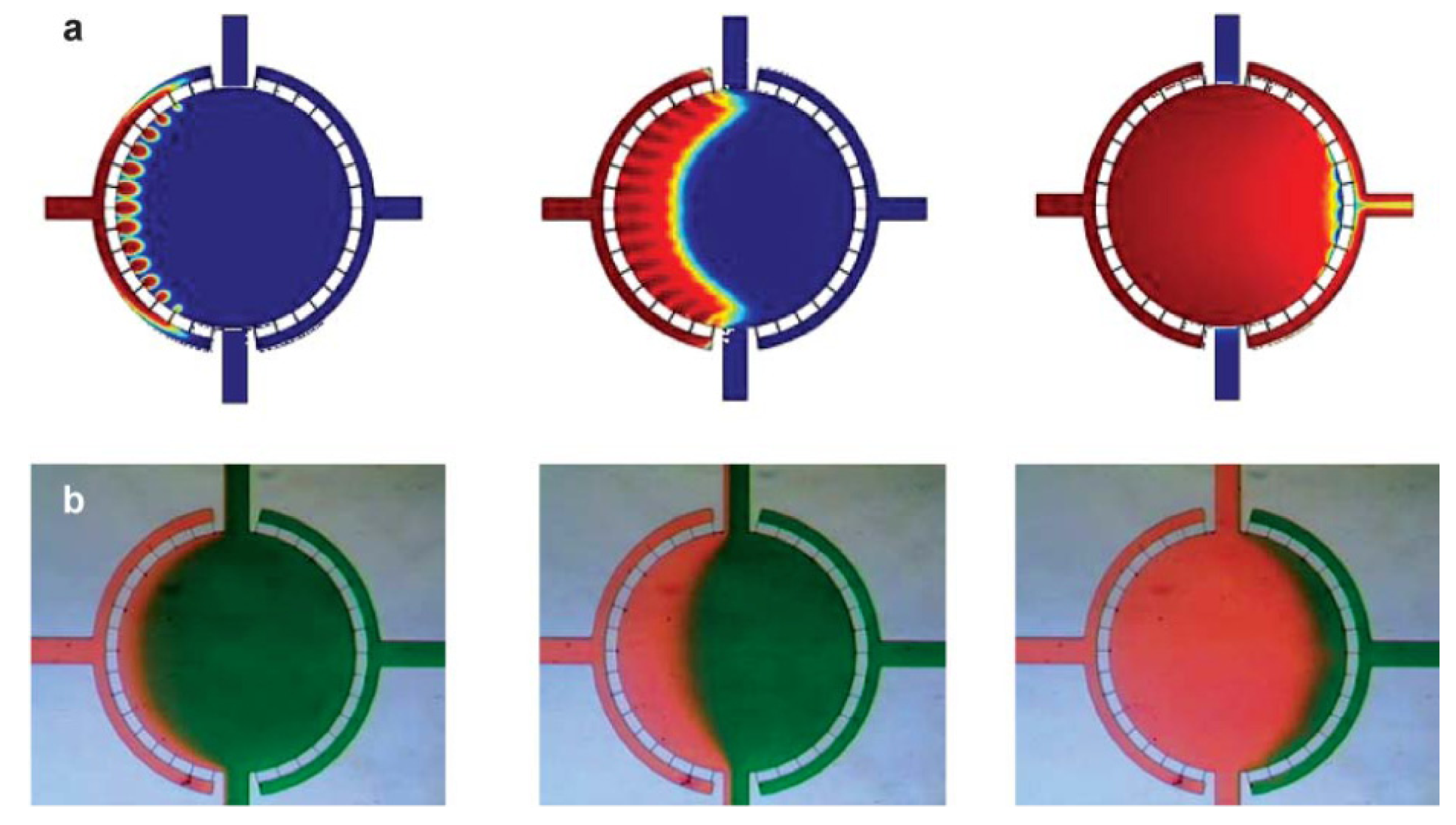
However, fluid flow analysis of these types of flow cells shows that the large plenums contain “dead” zones, where fluid stagnates, causing a larger residence time distribution within the flow cell. For systems containing reactive species, precipitates may form in dead zones, which inherently reduces the material utilization and can lead to clogging, which would alter the flow field across the flow cell.
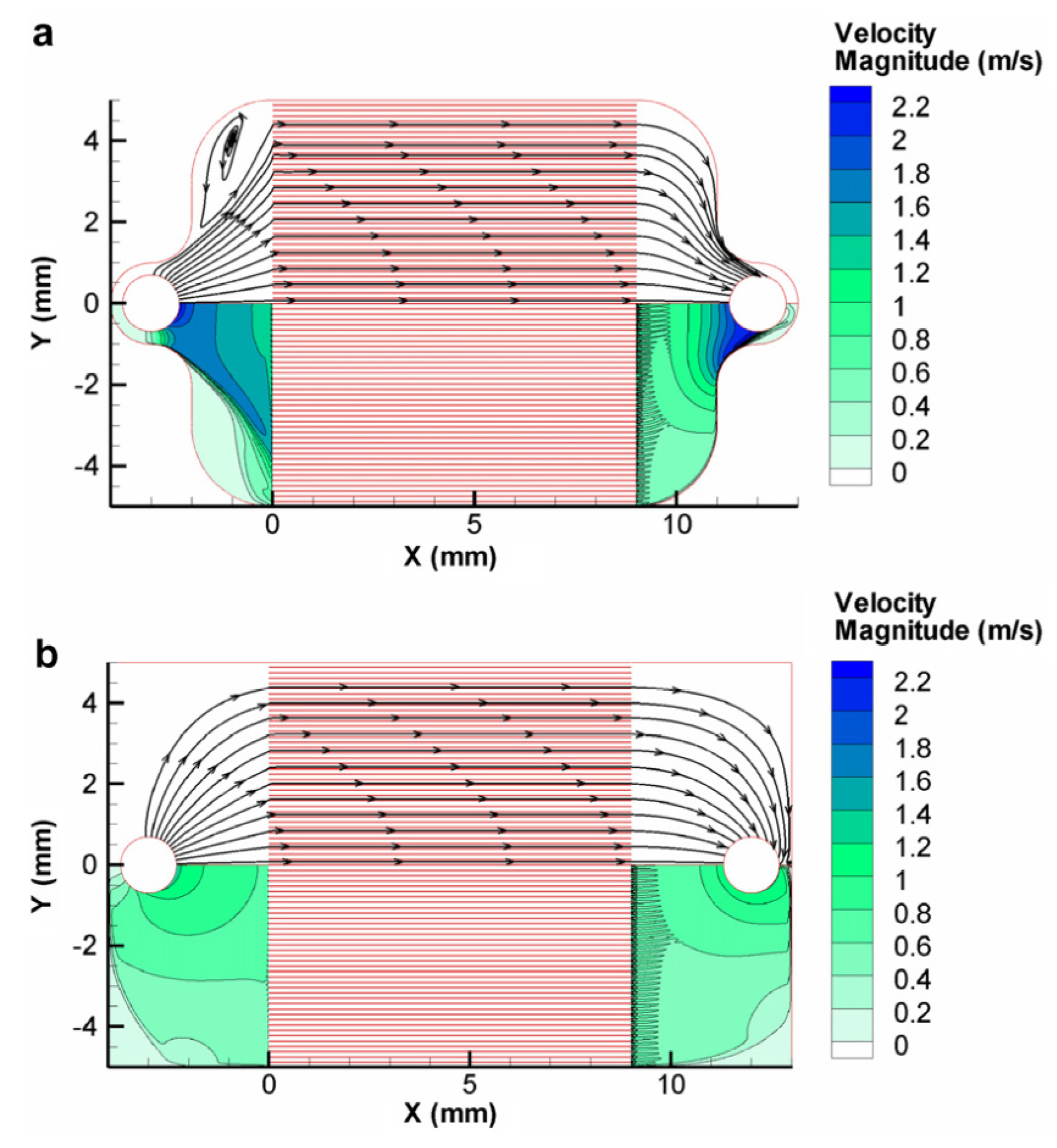
Jones
et al. investigated the flow distribution effects of the flow geometry in the plane parallel to the fluid plane of a microchannel heat sink [
60].
Figure 17 depicts the change in the velocity profile between two flow geometries; one with a constricted geometry around the inlet and outlet
versus a design with unconstrained flow from the inlet and outlet. Experimental analysis showed a much better flow distribution in the case of the unconstrained flow with a 4.7% difference between the maximum and minimum mass flux across the channel array for the unconstrained design
versus a 33.5% difference for the constrained design. The unconstrained design also realized a significantly lower pressure drop.
Figure 17.
Velocity contours of circular top down inlets. (
a) Constrained design around the inlet/outlet; (
b) Unconstrained design. Reproduced from [
60].
Figure 17.
Velocity contours of circular top down inlets. (
a) Constrained design around the inlet/outlet; (
b) Unconstrained design. Reproduced from [
60].
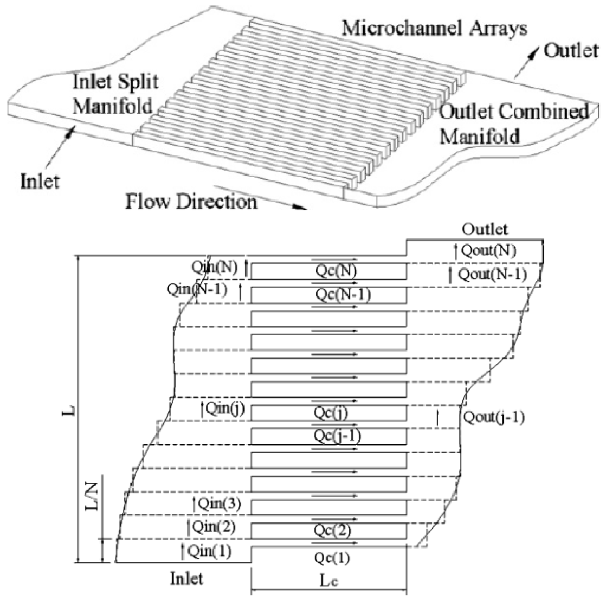
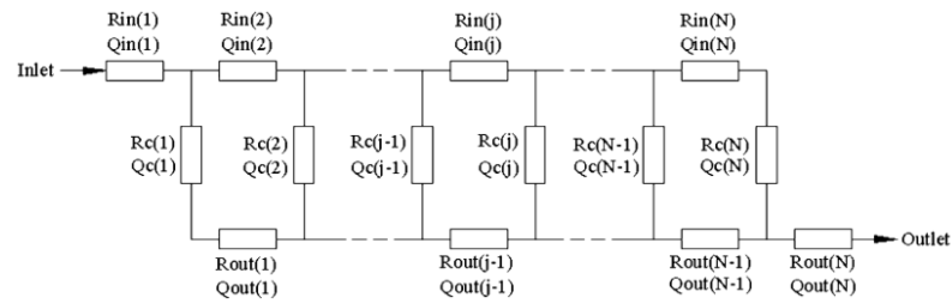
Pan
et al. characterized a microscale flow chamber composed of several parallel rectangular channels and used an electrical network parody to describe the system (
Figure 18) [
61].
Figure 18.
Microdevice design and analytical model. Reproduced from [
61].
Figure 18.
Microdevice design and analytical model. Reproduced from [
61].
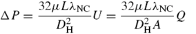
Operating under laminar flow conditions, the pressure drop of each channel using the Hagen–Poiseuille equation for rectangular channels is:
where
A is the channel cross-sectional area,
L is the channel length,
U is the velocity,
DH is the hydraulic diameter,
DH = 2
HW/(
H +
W); and λ
NC is a non-circular correction coefficient of (3/2)/((1 − 0.351(
E/
W))
2(1 +
H/
W)
2) for
W >
H. In the model, the “loop rule” of
V =
IR used for electrical circuits was made analogous to the Hagen–Poiseuille equation for fluidic circuits by replacing the voltage, current and electrical resistance with pressure drop, volumetric flow rate and the following term for flow resistance:
The basic overall resistance model assumes each channel is associated with its own unique inlet (
Rin) and outlet (
Rout) region, resulting in a unique potential difference (Δ
P) across each channel. This leads to a system of flow resistances in both series and in parallel, as shown in
Figure 19. Varying the length, depth and number of channels allowed the optimization of the inlet and outlet geometries for uniform a flow distribution between each channel.
Figure 19.
Microdevice design and the equivalent electrical resistance model. Reproduced from [
61].
Figure 19.
Microdevice design and the equivalent electrical resistance model. Reproduced from [
61].
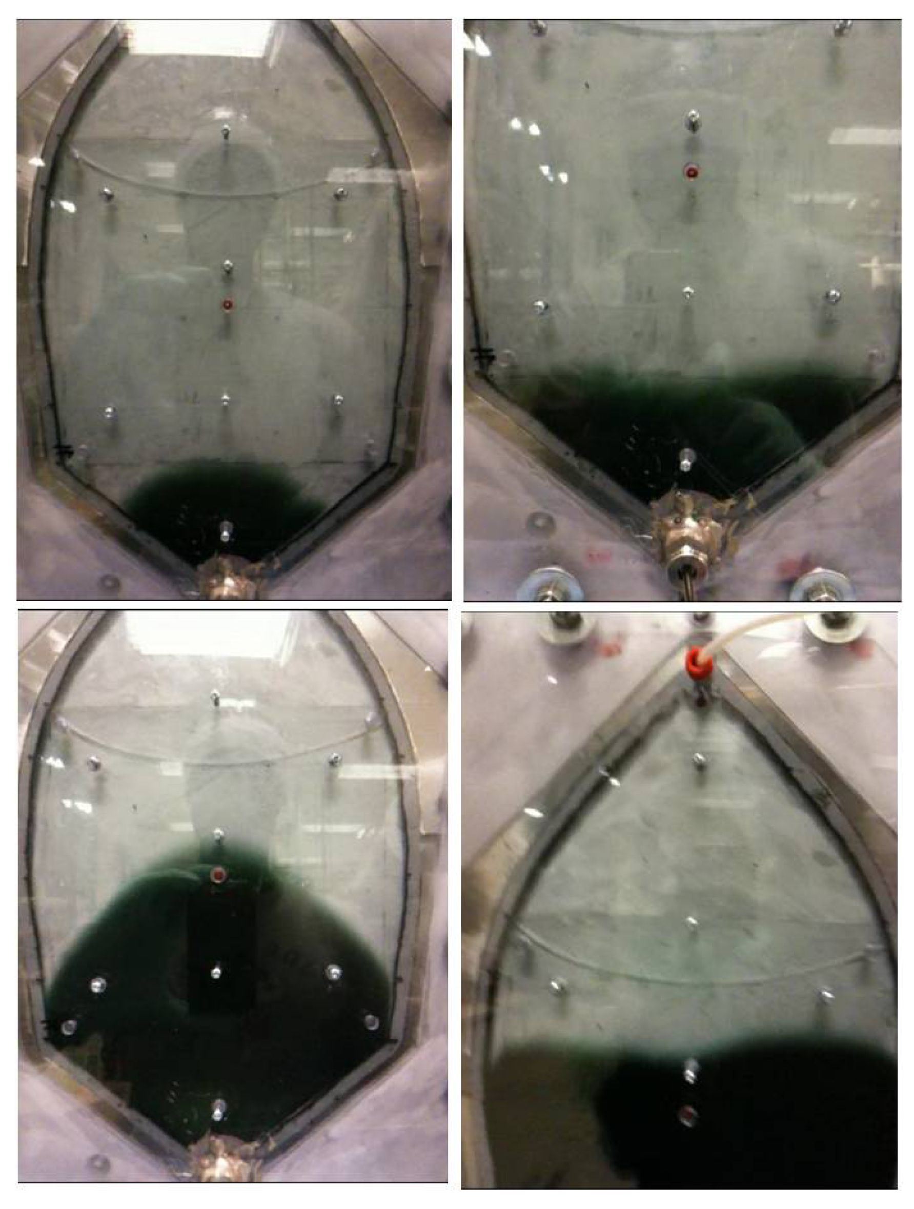
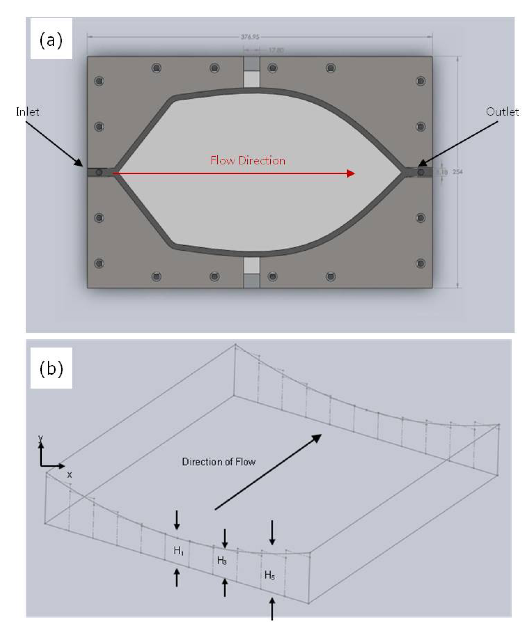
Paul
et al. developed a MASD flow cell with a more uniform fluid residence time for depositing CdS buffer layers for thin film photovoltaics over a 150 mm-sized glass substrate coated with fluorine-doped tin oxide (
Figure 20) [
49]. The geometry of the flow cell in the flow plane reflects efforts to minimize drag and stagnant flow regions within the flow cell. Similar to other flow cell designs, the height of the flow cell was controlled between 100 and 1000 μm by the distance between two parallel plates. However, in this design, the top plate was deflected into the flow cell, as shown in
Figure 20. The shape of the deflected channel profile was used to control the pressure drop of the fluid across the width of the flow channel, providing for a uniform flow front. Dye injection evaluations of flow fields within an 800 μm-high parallel plate and a deflected plate flow cell are shown in
Figure 21. The parallel plate flow cell shows a distinctive parabolic flow profile, while the deflected plate profile shows a much more uniform flow front both at the inlet and middle of the flow cell. The flow cell was used to produce CdS films between 20 and 40 nm in thickness with variations down to 10% across a 150 × 150-mm glass substrate. The thickness of the film deposited was found to be between three and five times more uniform than films produced using the parallel-plate flow cell. This level of film uniformity compared favorably with prior continuous reactor flow cells for solution deposition, showing over fivefold more variation in chemical product (nanowire) dimensions over a 30-mm dimension [
24].
Figure 20.
(
a) Top view of the MASD flow cell design and (
b) the deflected channel profile from the equivalent channel heights. Reproduced from [
49].
Figure 20.
(
a) Top view of the MASD flow cell design and (
b) the deflected channel profile from the equivalent channel heights. Reproduced from [
49].
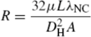
Figure 21.
Flow distributions at the beginning (
top) and middle (
bottom) of the flow cell for the parallel plate (
left) and the deflected plate (
right) flow cells. Reproduced from [
49].
Figure 21.
Flow distributions at the beginning (
top) and middle (
bottom) of the flow cell for the parallel plate (
left) and the deflected plate (
right) flow cells. Reproduced from [
49].

