
Evaluation of Relative Permittivity and Loss Factor of 3D Printing Materials for Use in RF Electronic Applications

Faculty of Engineering, Czech University of Life Sciences Prague, Kamycka 129, 165 00 Praha, Czech Republic
*
Author to whom correspondence should be addressed.
Processes 2022, 10(9), 1881; https://doi.org/10.3390/pr10091881
Submission received: 7 August 2022
/
Revised: 2 September 2022
/
Accepted: 14 September 2022
/
Published: 17 September 2022
(This article belongs to the Section Advanced Digital and Other Processes)
Abstract
:3D printing is more and more often used for the development and manufacturing of electronic devices and components. These applications require knowledge about the dielectric properties of the used materials—in particular minimal and stable values of relative permittivity and dielectric losses. The paper deals with the testing of the relative permittivity and loss factor of materials as follows: PLA (in three dye modifications), PET-G, and ABS and ASA in the frequency range 1–100 MHz. It was found that relative permittivity varied between 2.88–3.48 and the loss factor was in the range 0.03–4.31%. In terms of relative permittivity, all tested materials manifested a slight decline with increasing frequency. Concerning loss factor PLA (colorless) and ABS were proven to be more suitable for electrotechnical application due to the lower values and frequency dependences of the loss factor. Different results were observed in PLA-Silver and PLA-Metallic green. These materials showed a higher frequency dependency of loss factor with increasing frequency. The reasonable influence of added dyes was found. A study of the internal structure of the tested materials has not proven any significant defects (air gaps) that could affect the material’s dielectric properties.
1. Introduction
3D printing is now widespread manufacturing technology that has found applications in many different branches, such as the automotive industry, aerospace, medical instruments, spare parts manufacturing, and other sectors [1,2]. This technology is expanding across these different areas, especially because of rapid prototyping, which provides versatility and low production costs [3,4]. Another reason for the spread of fused deposition modeling (FDM) technology is the existence of the open-source RepRap project (self-replicating rapid prototype). This project has made the technology cheap and available to the general public, while at the same time current 3D printers based on the RepRap concept are capable of producing final products at a quality level comparable to those produced by commercial 3D printers [5,6]. The application of 3D printing technology in the manufacturing of electronic devices requires good information about the dielectric properties of the used materials. These materials should have constant relative permittivity and a low loss factor in the intended operating frequency range of the device, which means that they should be high-quality dielectric materials.
FDM is one of the most widely used 3D printing methods. These manufacturing methods are called additive manufacturing (AM) and can be defined as the process of layering manufacturing materials into the shape of designed objects [7]. FDM technology is a process based on the extrusion and deposition of filaments in multiple layers to create the final 3D object. The layers are joined by pressing and melting the surface of the previous layer during extrusion. When the molten material is extruded, it re-melts the portion of the existing layer and sticks tightly [8,9].
At present, FDM is more and more used for the development and manufacturing of electrotechnical components and devices. The main reason for this effort is to provide greater automation and flexibility of manufacturing with low production costs [10]. In electronics manufacturing, this technology can be used in several areas such as structural electronics [10,11], power electronics [12], high-frequency electronic applications [13,14], sensors fabrication [15], and smart textile [16].
Structural electronics in particular is becoming more interesting as this technology brings the possibility of automated production of electrical and electromechanical devices using a direct implementation of electrical components in printed objects [10,17]. It brings a more flexible, automated, and cheaper production [18].
Another technology sector that has recently undergone very rapid progressive development is the IoT (Internet of things). In this regard, 3D printing is also being used by a number of research laboratories in the production of dielectric components, for instance for antennas [19,20]. Two types of antennas are being tested in this field. The first one is based on a metalized structure that has been primarily printed from PLA. The second one is printed directly with conductive filament. Both of the methods have achieved good results with low production costs [21].
Another example of FDM application is smart textiles, which are defined as textiles that are able to sense, react and adapt to environmental stimuli. The stimuli and reactions can be magnetic, thermal, chemical, and electrical [22]. In this application, the use of electronic components requires mechanical, chemical, and temperature resistance and for this reason, it is necessary to ensure the encapsulation of their surfaces [23].
Further applications of 3D printing technology include the development and production of insulating components in electrical equipment. In particular, the development and production of biosensors and biocomponents using FDM is developing rapidly [24]. The same trends are evident in the field of capacitive sensors. Here, FDM brings the possibility of easily manufacturing very specific insulating electrode housings or electrode holders. An example of RF (radio frequency) electronic applications is the photomultiplier socket made by 3D printing, presented in Figure 1.
3D printing enables the creation of dielectric insulators of different shapes, and this process was used in a similar way in our work to develop a capacitive probe for measuring ice thickness. The evaluation of the capacitance of the developed sensor was performed by measuring the resonant frequency of the oscillator circuit to which the sensor was connected. These probe parts had to be made of a high-quality insulator with constant relative permittivity and a low loss factor in the frequency range of 3 to 10 MHz, which was the intended operating frequency range of the measuring device. For this reason, it is necessary to select suitable materials with appropriate dielectric properties.
For the above-described purposes, 3D printing materials must be studied in terms of their dielectric properties (e.g., electrical conductivity, permittivity, loss factor). The most commonly used materials for 3D printing are PET-G (polyethylene terephthalate glycol), PLA (polylactic acid), ABS (acrylonitrile butadiene styrene), and ASA (acrylonitrile styrene acrylate) [25,26]. Most recently published studies are focused on evaluating and comparing the mechanical [27,28] and thermal properties [29]. On the other hand, the studies aimed at the dielectric properties of materials processed by 3D printing are in the absolute minority. One of the points of interest in this area is studying how the printing settings change dielectric properties. This topic has been studied on PLA, ABS, and PET-G materials by Veselý et al. [7]. The authors tested the dielectric properties of these materials with printing resolutions of 50, 100, 150, and 200 µm in the low-frequency band (up to 100 kHz). They observed the drop-down of the relative permittivity with the increasing of printing layers (lower printing resolution) and the contemporary influence of the printing resolution on the loss factor was not significant. The permittivity and loss factor of printing materials are to some extent described in the range of low frequencies (50–100 Hz, and sporadically at 100 kHz) and at the band of ultra-high frequencies (1 GHz and higher). The frequency range of 3 to 10 MHz that is necessary to know for the development of our capacitive probe for measuring ice thickness has not been published yet. Dichtl et al. [3] studied the properties of PLA at frequencies from 1 to 3 GHz, but performed only two measurements (1 and 75 MHz) at higher frequencies. Deffenbaugh et al. [30] measured the dielectric properties of several 3D printing materials, including ABS in the 1 MHz to 11 GHz range, but in the 1 to 100 MHz range, he only performed three-point measurements at 1, 2, and 100 MHz.
It is important to realize that to replace missing values by the simple extrapolation of the known frequencies to the region frequencies that are distant from the exact tested ones is misleading because each relaxation process causes a drop in permittivity and a local increase in the loss factor in the dielectric material related to its time constant. The typical course of this phenomenon is shown in Figure 2 and Figure 3, where the drop in permittivity and increase in the loss factor due to the relaxation process with the time constant τ are shown. The dependencies were calculated by using the generally known Debye relations [31]. This influence is the most obviously pronounced at the angular frequency corresponding to the inverse value of the time constant. The phenomenon can be manifested in areas one decade-wide above and below this frequency. Polarization does not occur in more remote areas.
Therefore, it was not possible to deduce the properties of dielectrics in the field of high frequencies (HF) from the results of available publications and, moreover, the values of dielectric properties of the basic materials under the same condition published in different sources differ by tens of percent [32,33]. This phenomenon is probably caused by the manifestation of many relaxation processes in the materials themselves and especially by the presence of other composite admixtures. Therefore, it is necessary to become more acquainted with the properties of the materials used for 3D printing. This paper is focused on the comparison of dielectric properties such as loss factor and relative permittivity of the applied materials which have not been studied extensively yet. The secondary objective of this study was testing to verify that no significant defects (air gaps) had formed in the internal structure of the printed ABS, ASA, PETG, and PLA materials as a result of the deposition of individual layers during printing, which could affect the dielectric properties of the samples.
2. Materials and Methods
2.1. Tested Materials
In our study, we tested four types of the most commonly used materials for 3D printing: PLA, PETG, ABS, and ASA [25,26]. The PLA samples were made in three color modifications: colorless, silver, and metallic green. The reason why these color modifications were tested was to study the impact of the color dye additions on the dielectric properties of the materials. The PETG, ABS, and ASA samples were prepared in the colorless version only. The tested samples were printed as square plates with a side length of 70 mm and thickness of 2.5 mm (Figure 4).
The samples were prepared by a Prusa i3 MK3S+ 3D printer (Prusa Research, Prague, Czech Republic). This 3D printer is based on the FDM technology in RepRap concept. 3D printing was set to achieve the maximum density of the printed object. The setting of the printing parameters (resolution and fill density) determines the final density of the printed objects. The samples were printed at a resolution of 50 μm and a fill density of 100%. These printing settings should ensure the maximal possible homogeneity and density of the internal structure of the samples. The fill angle parameter was left at the default setting (45°). The filaments with a diameter of 1.75 mm manufactured by FilamentPM company (Czech Republic) were used for printing the samples. The samples’ parameters, including the printing settings, are summarized in Table 1.
2.2. Measuring of Dielectric Properties
The specific capacitor methodology was used to measure the dielectric parameters of the samples, in which the complex impedance of the capacitor was used to determine the complex permittivity of the sample dielectric. In the frequency range up to several hundred MHz, with the appropriate design of the measuring circuit, it can be analyzed as a lumped-parameters circuit. However, the parasitic parameters of the interconnection network between the measuring capacitor and the complex impedance analyzer must always be considered. At higher frequencies (usually 0.3 to 1 GHz), where the dimensions of the measuring circuit and its individual elements are comparable to the wavelength of the measuring signal, the circuit must be designed as a circuit with distributed parameters. The dielectric sample is placed in a circuit in which the electromagnetic wave is excited and the dielectric properties of the circuit are derived from the changes in the properties of the circuit caused by the measured sample [34].
The complex impedance samples were measured by the Agilent E4991A RF Impedance/Material analyzer. Probe 16453A, which is normally supplied by the manufacturer, was not used as the measuring capacitor. The probe is only suitable for measuring thin samples. The manufacturer guarantees a measurement accuracy of only tens of percent for samples with a thickness of a few millimeters [35]. Therefore, a measuring probe of our own design was used with electrodes that were significantly larger in surface area (approximately 100 times), and this had an impedance with our measured samples that corresponded to the area in which the analyzer could achieve maximal accuracy.
The testing device is shown in Figure 5. It consisted of the above-mentioned Agilent analyzer and the measuring probe with the analyzed sample.
The tested relative permittivity and the loss factor were evaluated in the frequency range of 1–100 MHz (at approximately 200 measuring points). The circuit diagram of the measuring is shown in Figure 6. The measuring device provides the circuit parameters—total capacitance (Cp) and its quality factor (Q). The relation between these two parameters describes Equation (1). The loss factor (tgδ) is then calculated from the data (Q) according to the following relation (2).
where: Q—capacitance quality factor [-], Cp—total capacitance of the measured system [F], R—parallel loss resistance of the sample [Ω], tgδ—loss factor of the sample [%], and Cs—capacitance of the measured sample [F]. The value of the relative permittivity was determined proportionally from the capacitance of examined sample and the capacitance of the Teflon standard. Conversion was performed using Equation (3):
where: Ct—capacitance of the Teflon control sample [pF], εr—relative permittivity of the measured sample [-], εt—relative permittivity of Teflon (2.1), ts—sample thickness [mm], and tt—Teflon standard thickness (1 mm). The parasitic capacitances of the interconnection network Cpar and the parasitic inductance of the network Lpar were automatically compensated by the impedance analyzer E4991A. Compensation was performed on the basis of impedance analysis of the interconnection network with the sample disconnected, and a short-circuit or open circuit at its terminals. Compensation led to a transfer of the measuring interface from the terminals of the measuring instrument to the sample terminals, thus eliminating the influence of parasitic parameters of the interconnection network [36].
2.3. Data Processing
The raw data were used for the evaluation of the relative permittivity and loss factor. The measurement interval of the loss factor was divided into three intervals (1–19.9, 20–59.9, and 60–100 MHz) for a more precise description of the measured material parameters. The relative permittivity data did not show such large changes in the measured range (1–100 MHz) and for this reason, the data were not divided into multiple intervals. The average and standard deviations of the relative permittivity and loss factor were calculated for each interval.
2.4. Testing of the Presence of Defects in the Internal Structure of Samples
The internal structures of PLA (colorless), PETG, ABS, and ASA material samples were tested. The aim was to verify the absence of significant defects (air gaps) in these samples as a consequence of the layering of individual filaments during the printing process. These defects could subsequently significantly affect the dielectric properties of the final samples.
Sample preparation consisted of deep and rapid freezing of individual samples in a bath of liquid nitrogen. The deep-frozen samples were fixed and broken by a fast impact. The break was performed in the plane of the diagonal of the samples, in the same direction that the individual filaments deposited during printing (fill angle 45°). Some of the samples prepared by this method were subsequently ground (water-cooled grinding). The two prepared break surfaces, the ground and pure break surfaces, were subsequently studied under a microscope.
3. Results
The results are presented in the following figures (Figure 7, Figure 8, Figure 9 and Figure 10). All statistically processed data are presented in Table 2 and Table 3. The graphs in Figure 7 and Figure 8 express the frequency relations of the relative permittivity of the tested materials. Figure 7 describes the frequency dependence of the relative permittivity of the colorless materials (PLA, PETG, ABS, and ASA). It can be seen that the values of permittivity in the interval 1–100 MHz amounted to 2.9–3.48. The curves of ASA and PETG were practically identical and the difference between these two materials was approximately 0.1 in the entire measuring range. The second pair of results included the measurements of ABS and PLA, which displayed very similar behavior, with mutual differences at only 0.06. Throughout the frequency range, the value of permittivity changed insignificantly with a practically linear shape in all the curves and a slight tendency to decrease with the increasing frequency was recorded. The graph in Figure 8 expresses the comparison of the frequency dependence of PLA materials with a different color. It can be seen that the relative permittivity values were in the range of 2.88 to 3.47. According to the graph (Figure 8), PLA and PLA-Silver had almost identical curves. The only difference was the fact that PLA (colorless material) had lower frequency dependence. Out of the PLA materials, PLA-Metallic green achieved higher values over the entire frequency range. The approximate difference between PLA and PLA-Metallic green was estimated at 0.36. The average value of PLA was estimated to be 3.00, PLA-Silver 2.99, and PLA-Metallic green 3.36 (Table 2). The relative permittivity of PLA and PLA-Silver was found to be practically identical, but PLA-Metallic green differed in its absolute permittivity value, with the slope of the curve being the same (with a slight drop in relative permittivity with a higher frequency).
The frequency dependence of the loss factor of all tested materials is summarized in the following graphs (Figure 9 and Figure 10). The graph in Figure 9 describes the frequency dependence of the loss factor of the colorless materials. According to this graph, the loss factor was in the interval of 0.03–2.21%. PLA and ABS curves were practically identical in shape over the entire frequency range, with absolute value differences of approximately only 0.2%. The trend in the relation between these two materials is the slow drop in loss factor values with increasing frequency. The other two materials (PETG and ASA) put together the second group of materials with a very similar frequency dependence of the loss factor. The only difference in the trend between these two materials was observed in the frequency range 1–10 MHz, where the ASA curve displayed a mild drop compared to PETG. However, in the rest of the frequency range, the trend for both materials was declining. The differences in absolute values between PETG and ASA were estimated at 0.32%.
Figure 10 compares the loss factor frequency dependency of the PLA materials with different color pigmentation. The loss factor values ranged from 0.03 to 4.31% in the frequency interval studied. PLA-Silver and Metallic Green curves showed a similar overall shape with a slightly increasing absolute value of the loss factor in the higher frequency region. The maximal increase was observed in the range of 70–100 MHz. However, these two curves differed substantially in their shape in the 1–20 MHz interval. Here, the relatively significant and linear increase in the loss factor was found in PLA-Silver as compared to PLA-Metallic green. Both of the curves had similar and parallel shapes from the 20 MHz frequency. On the other hand, the PLA curve showed a drop in the frequency dependence of the loss factor with increasing frequency.
The average values of the relative permittivity of tested materials in the related frequency range are summarized in Table 2. Directly measured data were statistically processed (average and standard deviation) and in this manner, the tabulated data were provided for potential practical use. In the range of 1–100 MHz, the average values were estimated in the interval of 2.99 (PLA-Silver) to 3.36 (Metallic green). The relative permittivity values of the PLA and PLA-Silver were almost identical (Table 2), and the differences between the PLA (colorless material) and PLA-Metallic green were estimated at 0.36.
Values of the loss factor in the assessed frequency intervals are summarized in Table 3. The tested frequency range was divided into three intervals: 1–19.9, 20–59.9, and 60–100 MHz. Directly measured data were then statistically processed (average and standard deviation). The colorless materials achieved maximum loos factor values in the frequency range 1–19.9 MHz and minimum values in the range 60–100 MHz (Table 3). On the other hand, the colored PLA materials showed minimum values in the range of 1–19.9 MHz and a maximum in the interval of 60–100 MHz. The maximal difference between the loss factors of the three types of tested PLA materials was observed between the PLA (colorless) and PLA-Silver, which reached 0.87% (1–19.9 MHz), 2.13% (20–59.9 MHz), and 3.06% (60–100 MHz). Naturally, the data in Table 2 and Table 3 fully correspond to the data in the graphs (Figure 7, Figure 8, Figure 9 and Figure 10).
The next parameter examined was tested to verify that no significant defects (air gaps) had formed in the internal structure of the samples as result of the deposition of individual layers during printing, which could affect the dielectric properties of the samples. The results are shown in Figure 11, which summarizes microscope images of the break surfaces of each of the tested materials ABS, ASA, PETG, and PLA (colorless). Figure 11A,C,E,G show the break surfaces of ABS, ASA, PETG, and PLA (colorless). Figure 11B,D,F,H display the ground break surfaces of ABS, ASA, PETG, and PLA materials (colorless). From these individual cuts, it is obvious that no significant defects (air gaps) of the internal structure were presented in the tested materials.
4. Discussion
The presented data show that the relative permittivity values varied between 2.88–3.48 and the loss factor values ranged from 0.03–4.31%. These results mean that all the materials tested showed a very slight decrease in relative permittivity with increasing frequency. Indeed, comparing the relative permittivity of PLA materials, the PLA colorless and PLA-Silver had almost identical frequency dependence over the entire measurement range. On the other hand, PLA-Metallic green had an approximately 0.36 higher relative permittivity values over the entire frequency range, but the general shape of the curves was the same for both materials. The difference was probably caused by pigment dye added to the PLA-Metallic green.
According to the measured data, the loss factor of these colorless materials was determined to be in the range of 0.03–2.21%, and the PLA color materials (PLA-Silver and Metallic green) were in the range of 0.71–4.31%. The colorless materials showed significantly lower interval variation and much lower frequency dependence. The lowest values of the loss factor and its minimal frequency dependence were observed in colorless PLA, which made this material the most suitable for electrical applications among those tested here. The second one which appears to be useful for these applications is the ABS. Similar to the PLA, ABS achieved the low-frequency dependence of the loss factor, but the absolute values were rather higher. On the other hand, the PETG and ASA were proven to have the highest loss factor values in terms of colorless materials in the range of 1–5 (PET-G) and 5–100 MHz (ASA). The frequency dependence of PETG and ASA was minimal in the entire frequency range. Both colored PLA materials had the least suitable parameters in terms of use for electrical applications. The significant frequency dependence of the loss factor over the entire measuring range was proven. These results are in concordance with the above-mentioned ones of Dichtl et al. [3] and Deffenbaugh et al. [30]. The higher values of the loss factor in the range 20–100 MHz were observed in PLA-Silver (Table 3): 2.28% (20–59.9 MHz) and 3.13% (60–100 MHz). Another difference between PLA (colorless) and the colored PLA samples is the trend of the loss factors curves. For PLA and similarly for other colorless materials, the declining trend of the loss factor values was more frequent, but the colored materials achieved the opposite trend.
Differences between colored and colorless materials are probably caused by the additives pigment dyes which significantly influenced the dielectric parameters of the materials. It is known that conductive pigment dyes cause a decrease in the high-frequency resistance of the material. This is caused by the influence of the contact resistance of connecting grains of the dye. Due to their inhomogeneous distribution, the current tracks are not continuous and at low concentrations of the conductive substance, its effect on the DC resistance is significantly smaller. Non-conductive dyes cause an increase in the loss factor of the composite dielectric due to their own losses. Dyes contained in plastic materials increase the loss factor and cause other polarization processes, especially at frequencies of the order of tens and hundreds of MHz. Pure materials (without dyes) showed polarizations with a time constant in the range of milliseconds which led to a slight increase in relative permittivity and a strong increase in loss factor (tgδ) in the low frequency ranges (hundreds of Hz to kHz) [31]. The influence of dielectric properties of the 3D printing materials has been described by Veselý et al. [25] and Balakrishnan et al. [37] as well. Balakrishnan et al. [37] observed the significant influence of the pigment dyes on conductivity of PLA materials. A similar effect of the pigment dyes on the properties of the materials for 3D printing was studied by Castro et al. [38] and Wittbrodt et al. [6]. They proved that pigmentation had a significant influence on a material’s mechanical properties.
According to the tested break surfaces of ABS, ASA, PETG, and PLA (colorless), the presence of significant defects (air gaps) in the internal structure of the samples formed during their printing, which could affect their dielectric properties, was not proven.
5. Conclusions
3D printing is a widespread and rapidly developing technology that provides rapid prototyping and low-cost production, and for this reason its application is found in many different areas. Currently, 3D printing is more and more frequently used for the development and manufacturing of electrotechnical components and devices. These applications require knowledge about the dielectric properties of the used materials proceeded by 3D printing technology.
The paper dealt with the comparison of dielectric properties such as relative permittivity and a loss factor of PLA, PET-G, ABS, and ASA materials. The PLA materials samples were prepared in three different color sets for the comparison of the pigment dye on the above-mentioned material properties. The parameters were measured in the frequency range of 1–100 MHz and the results were as follows:
- The absence of polarization phenomena was proven for the tested colorless materials in the range of 1–100 MHz. This absence of the polarization phenomena was manifested by the insignificant frequency dependence of the dielectric properties of these materials;
- The values of relative permittivity varied between 2.88–3.48 and the values of loss factor were in the range of 0.03–4.31%;
- In terms of relative permittivity, all the tested materials showed minimal frequency dependence in the entire measuring range with a slight tendency to decrease in the higher frequency range. The minimal values of relative permittivity reached ABS (2.95), PLA (3.00), and PLA-Silver (2.99), which proved nearly identical parameters. On the other hand, PLA-Metallic green reached a value of 0.36 higher than PLA. This phenomenon was probably caused by added pigment dye;
- In terms of the loss factor, PLA and ABS appeared to be more suitable for electrotechnical application due to lower values and lower frequency dependencies of the loss factor in all studied frequency ranges. The values of the loss factor of PLA and ABS were estimated at: 0.51%, 0.77% (1–19.9 MHz); 0.15%, 0.38% (20–59.9 MHz), and 0.07%, and 0.21% (60–100 MHz);
- PET-G and ASA showed higher values and frequency dependence of the loss factor, and, for this reason, these two materials were less useful for electrotechnical application;
- The loss factor of PLA-Silver and PLA-Metallic green had significant frequency dependence, which was evident at higher frequencies. This increase was most evident in the upper part of the frequency range (70–100 MHz). In these intervals, PLA-Silver and PLA-Metallic green reached the maximum values of loss factor (4.31% and 3.24%). Due to these facts, these materials were inferior for electrotechnical applications;
- Significant differences were observed between PLA (colorless), PLA-Silver, and PLA-Metallic green, considering the loss factor. They can be caused by pigment dye which increases the values and frequency dependence and brings limitations for the use of these materials in electrical applications;
- PLA and ABS were more suitable for electrotechnical applications. They reached the smallest values of relative permittivity and loss factor, and at the same time, they proved the minimal frequency dependence of the tested parameters on the studied frequency range;
- The presence of significant defects (air gaps) in the internal structure of the printed samples of ABS, ASA, PETG, and PLA, which would affect their dielectric properties, were not proven.
Further research could focus on the effect of 3D printing technology on the electrical strength of processed materials and their aging caused by high electric field strength.
Author Contributions
Conceptualization, T.P. and S.P. (Stanislava Papezova); methodology, S.P. (Stanislava Papezova); validation, T.P. and S.P. (Stanislava Papezova); formal analysis, T.P.; investigation, T.P. and S.P. (Stanislava Papezova); resources, T.P. and S.P. (Stepan Picha); data curation, T.P. and S.P. (Stanislava Papezova); writing—original draft preparation, T.P.; writing—review and editing, S.P. (Stanislava Papezova); visualization, T.P. and S.P. (Stepan Picha); supervision, S.P. (Stanislava Papezova); project administration, T.P.; funding acquisition, T.P. All authors have read and agreed to the published version of the manuscript.
Funding
This research and the APC were funded by the internal research project of the Czech University of Life Sciences Prague, Faculty of Engineering: Analysis of operating parameters of electric vehicles, NO.: 2020:31150/1312/3102.
Data Availability Statement
The data presented in this study are available in the article.
Acknowledgments
The authors thank the CTU in Prague, Faculty of Electrical Engineering, for enabling the measurement of the quality factor and the total capacity of the tested samples.
Conflicts of Interest
The authors declare no conflict of interest.
References
- Ning, F.; Cong, W.; Wei, J.; Wang, S.; Zhang, M. Additive Manufacturing of CFRP Composites Using Fused Deposition Modeling: Effects of Carbon Fiber Content and Length. In Proceedings of the ASME 2015 International Manufacturing Science and Engineering Conference MSEC2015, Charlotte, NC, USA, 8 June 2015; American Society of Mechanical Engineers: Charlotte, NC, USA, 2015. [Google Scholar]
- Vujović, I.; Šoda, J.; Kuzmanić, I.; Petković, M. Parameters Evaluation in 3D Spare Parts Printing. Electronics 2021, 10, 365. [Google Scholar] [CrossRef]
- Dichtl, C.; Sippel, P.; Krohns, S. Dielectric Properties of 3D Printed Polylactic Acid. Adv. Mater. Sci. Eng. 2017, 2017, 6913835. [Google Scholar] [CrossRef]
- Felício, J.M.; Fernandes, C.A.; Costa, J.R. Complex Permittivity and Anisotropy Measurement of 3D-Printed PLA at Microwaves and Millimeter-waves. In Proceedings of the 2016 22nd International Conference on Applied Electromagnetics and Communications (ICECOM), Dubrovnik, Croatia, 19–21 September 2016; Instituto Superior Técnico: Dubrovnik, Croatia, 2016; pp. 1–6. [Google Scholar]
- Tymrak, B.M.; Kreiger, M.; Pearce, J.M. Mechanical properties of components fabricated with open-source 3-D printers under realistic environmental conditions. Mater. Des. 2014, 58, 242–246. [Google Scholar] [CrossRef]
- Wittbrodt, B.T.; Pearce, J.M. The effects of PLA color on material properties of 3-D printed components. Addit. Manuf. 2015, 8, 110–116. [Google Scholar] [CrossRef]
- Veselý, P.; Tichý, T.; Sefl, O.; Hornyová, E. Evaluation of dielectric properties of 3D printed objects based on printing resolution. In IOP Conference Series: Materials Science and Engineering; IOP Publishing: Bristol, UK, 2018. [Google Scholar]
- Patterson, A.E.; Pereira, T.R.; Allison, J.T.; Messimer, S.L. IZOD impact properties of full-density fused deposition modeling polymer materials with respect to raster angle and print orientation. In Proceedings of the Institution of Mechanical Engineers, Part C: Journal of Mechanical Engineering Science; SAGE Publications Ltd.: Thousand Oaks, CA, USA, 2019. [Google Scholar]
- FDM 3D Printing—Fused Deposition Modeling Ultimate Guide. Available online: https://electroloom.com/fdm-3d-printing-and-printer-guide/ (accessed on 19 August 2022).
- Espalin, D.; Muse, D.W.; Macdonald, E.; Wicker, R.B. 3D Printing multifunctionality: Structures with electronics. Int. J. Adv. Manuf. Technol. 2014, 72, 963–978. [Google Scholar] [CrossRef]
- MacDonald, E.; Salas, R.; Espalin, D.; Perez, M.; Aguilera, E.; Muse, D.; Wicker, R.B. 3D printing for the rapid prototyping of structural electronics. IEEE Access 2014, 2, 234–242. [Google Scholar] [CrossRef]
- Liu, Z.; Li, W.-D.; Wang, Y.-B.; Su, G.-Q.; Zhang, G.-J.; Cao, Y.; Li, D.-C. Topology optimization and 3D-printing fabrication feasibility of high voltage FGM insulator. In ICHVE 2016–2016 IEEE International Conference on High Voltage Engineering and Application; Institute of Electrical and Electronics Engineers Inc.: Chengdu, China, 2016; pp. 1–4. [Google Scholar]
- Colella, R.; Chietera, F.P.; Catarinucci, L. Analysis of FDM and DLP 3D-Printing Technologies to Prototype Electromagnetic Devices for RFID Applications. Sensors 2021, 21, 897. [Google Scholar] [CrossRef]
- Pizarro, F.; Salazar, R.; Rajo-Iglesias, E.; Rodriguez, M.; Fingerhuth, S.; Hermosilla, G. Parametric Study of 3D Additive Printing Parameters Using Conductive Filaments on Microwave Topologies. IEEE Access 2019, 7, 106814–106823. [Google Scholar] [CrossRef]
- Khosravani, M.R.; Reinicke, T. 3D-printed sensors: Current progress and future challenges. Sens. Actuators A Phys. 2020, 305, 111916. [Google Scholar] [CrossRef]
- Kalaš, D.; Šíma, K.; Kadlec, P.; Polanský, R.; Soukup, R.; Řeboun, J.; Hamáček, A. FFF 3D Printing in Electronic Applications: Dielectric and Thermal Properties of Selected Polymers. Polymers 2021, 13, 3702. [Google Scholar] [CrossRef]
- Lopes, A.J.; MacDonald, E.; Wicker, R.B. Integrating stereolithography and direct print technologies for 3D structural electronics fabrication. Rapid Prototyp. J. 2012, 18, 129–143. [Google Scholar] [CrossRef]
- Palmer, J.A.; Jokiel, B.; Nordquist, C.D.; Kast, B.A.; Atwood, C.J.; Grant, E.; Livingston, F.J.; Medina, F.; Wicker, R.B. Mesoscale RF relay enabled by integrated rapid manufacturing. Rapid Prototyp. J. 2006, 12, 148–155. [Google Scholar] [CrossRef]
- Le Sage, G.P. 3D Printed Waveguide Slot Array Antennas. IEEE Access 2016, 4, 1258–1265. [Google Scholar] [CrossRef]
- Rashidian, A.; Shafai, L.; Sobocinski, M.; Perantie, J.; Juuti, J.; Jantunen, H. Printable Planar Dielectric Antennas. IEEE Trans. Antennas Propag. 2016, 64, 403–413. [Google Scholar] [CrossRef]
- Helena, D.; Ramos, A.; Varum, T.; Matos, J.N. The Use of 3D Printing Technology for Manufacturing Metal Antennas in the 5G/IoT Context. Sensors 2021, 21, 3321. [Google Scholar] [CrossRef]
- Proesmans, R.; Verleysen, A.; Vleugels, R.; Veske, P.; De Gusseme, V.L.; Wyffels, F. Modular Piezoresistive Smart Textile for State Estimation of Cloths. Sensors 2021, 22, 222. [Google Scholar] [CrossRef]
- Kalas, D.; Suchy, S.; Kalcik, J.; Reboun, J.; Soukup, R.; Hamacek, A. Contacting of SMD Components on the Textile Substrates. In Proceedings of the International Spring Seminar on Electronics Technology, Demanovska Valley, Slovakia, 14–15 May 2020; pp. 1–6. [Google Scholar]
- Remaggi, G.; Zaccarelli, A.; Elviri, L. 3D Printing Technologies in Biosensors Production: Recent Developments. Chemosensors 2022, 10, 65. [Google Scholar] [CrossRef]
- Veselý, P.; Horynová, E.; Tichý, T.; Šefl, O. Study of electrical properties of 3D printed objects. In Proceedings of the International Student Scientific Conference Poster—22/2018; Husník, L., Ed.; Czech Technical University in Prague: Prague, Czech Republic, 2018; pp. 1–5. [Google Scholar]
- Kumar, S.R.; Sridhar, S.; Venkatraman, R.; Venkatesan, M. Polymer additive manufacturing of ASA structure: Influence of printing parameters on mechanical properties. In Proceedings of the 2nd International Conference on Recent Trends in Metallurgy, Materials Science and Manufacturing (IMME), Tiruchirappalli, India, 12–13 December 2019; pp. 1316–1319. [Google Scholar]
- Cojocaru, V.; Frunzaverde, D.; Miclosina, C.-O.; Marginean, G. The Influence of the Process Parameters on the Mechanical Properties of PLA Specimens Produced by Fused Filament Fabrication— A Review. Polymers 2022, 14, 886. [Google Scholar] [CrossRef]
- Maszybrocka, J.; Dworak, M.; Nowakowska, G.; Osak, P.; Łosiewicz, B. The Influence of the Gradient Infill of PLA Samples Produced with the FDM Technique on Their Mechanical Properties. Materials 2022, 15, 1304. [Google Scholar] [CrossRef]
- Le, T.-H.; Le, V.-S.; Dang, Q.-K.; Nguyen, M.-T.; Le, T.-K.; Bui, N.-T. Microstructure Evaluation and Thermal–Mechanical Properties of ABS Matrix Composite Filament Reinforced with Multi-Walled Carbon Nanotubes by a Single Screw Extruder for FDM 3D Printing. Appl. Sci. 2021, 11, 8798. [Google Scholar] [CrossRef]
- Deffenbaugh, P.I.; Rumpf, R.C.; Church, K.H. Broadband microwave frequency characterization of 3-d printed materials. IEEE Trans. Compon. Packag. Manuf. Technol. 2013, 3, 2147–2155. [Google Scholar] [CrossRef]
- Havriliak, S.; Havriliak, S.J. Dielectric and Mechanical Relaxation in Materials, Analysis, Interpretation, and Application to Polymers; Hanser Publishers: Munich, Germany, 1997; pp. 378–400. [Google Scholar]
- Novac, O.C.; Maries, G.R.E.; Chira, D.; Novac, M. Study concerning the influence of the grinding percentage on some electrical properties of PA 6.6, POM and ABS by methods for determining relative permittivity and the dielectric dissipation factor. Mater. Plast. 2017, 54, 453–460. [Google Scholar] [CrossRef]
- Booth, J.C.; Whitley, M.; Rudd, C.; Kranz, M. Material Database for Additive Manufacturing Techniques; Defense Technical Information Center: Fort Belvoir, VA, USA, 2017; pp. 1–37.
- Ctibor, P.; Sedláček, J.; Papež, V.; Lukáč, F. Radiofrequency and Microwave Dielectric Properties of Plasma Sprayed and Annealed Thick Layers of Titanium Dioxide. J. Therm. Spray Technol. 2020, 29, 1718–1727. [Google Scholar] [CrossRef]
- Agilent Technologies Inc. Agilent E4991A RF Impedance/Material Analyzer Data Sheet; Agilent Technologies Inc.: Santa Clara, CA, USA, 2003; pp. 6–7. [Google Scholar]
- Agilent Technologies Inc. Agilent E4991A RF Impedance/Material Analyzer Installation and Quick Start Guide; Agilent Technologies Inc.: Santa Clara, CA, USA, 2012; pp. 73–80. [Google Scholar]
- Balakrishnan, N.K.; Koenig, K.; Seide, G. The Effect of Dye and Pigment Concentrations on the Diameter of Melt-Electrospun Polylactic Acid Fibers. Polymers 2020, 12, 2321. [Google Scholar] [CrossRef] [PubMed]
- Castro, F.; Santana, L.; Lino Alves, J. Extrusion-Based 3D Printing: Color Influence on Mechanical Properties of PLA Parts. In COBEM—26th International Congress of Mechanical Engineering at: Florianópolis, Brasil; Associacao Brasileira de Engenharia e Ciencias Mecanicas—ABCM: Florianópolis, Brasil, 2021. [Google Scholar]
Figure 1.
Example of the FDM application to RF electronic—photomultiplier socket made by 3D printing.
Figure 1.
Example of the FDM application to RF electronic—photomultiplier socket made by 3D printing.
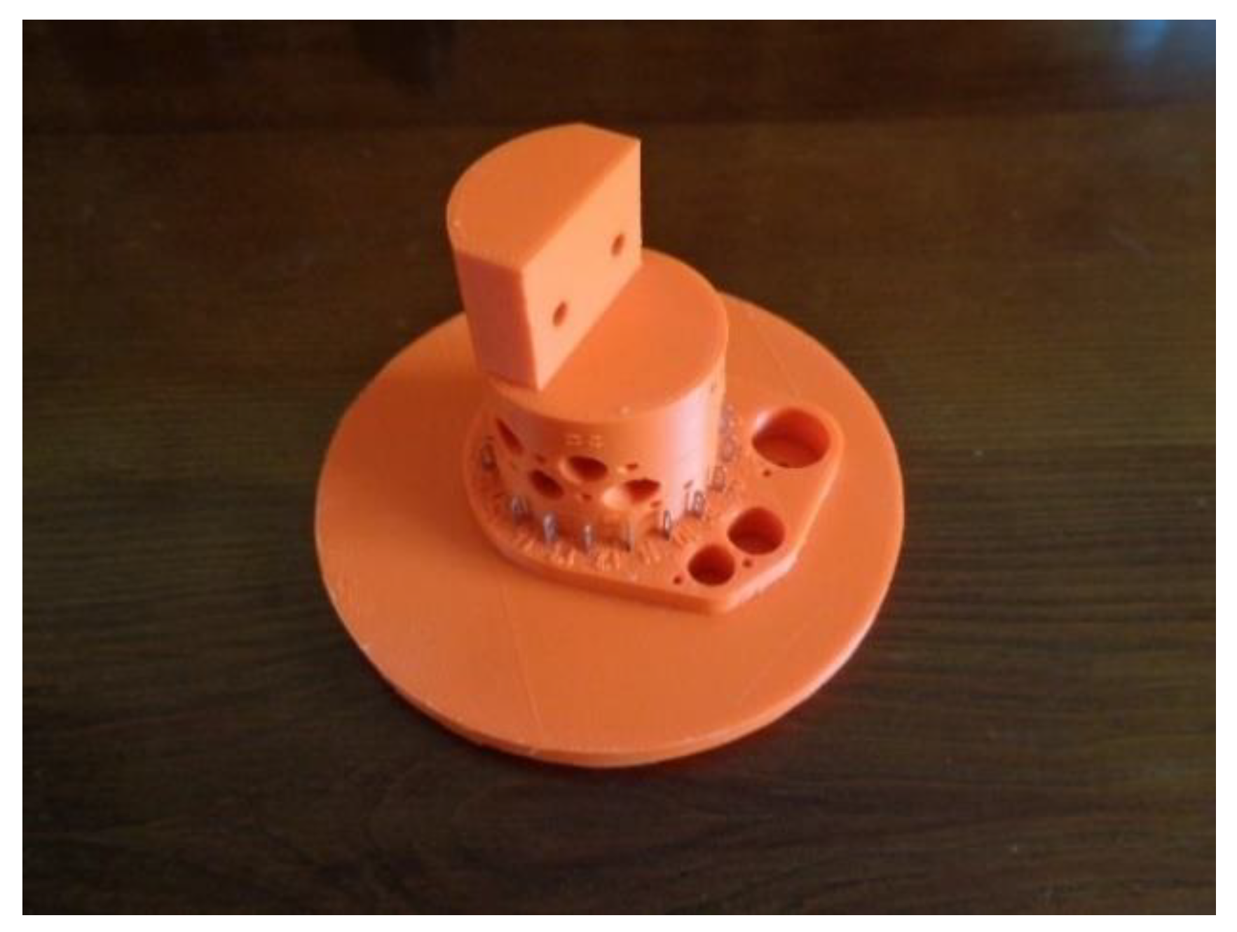
Figure 2.
Frequency dependence of normalized relative permittivity: τ—time constant of the relaxation process, εS—relative permittivity for low frequencies with respect to the relaxation frequency, ε∞—relative permittivity for high frequencies with respect to the relaxation frequency.
Figure 2.
Frequency dependence of normalized relative permittivity: τ—time constant of the relaxation process, εS—relative permittivity for low frequencies with respect to the relaxation frequency, ε∞—relative permittivity for high frequencies with respect to the relaxation frequency.
Figure 3.
Frequency dependence of the loss factor tgδ: τ—time constant of relaxation process, εS—relative permittivity for low frequencies with respect to the relaxation frequency, ε∞—relative permittivity for high frequencies with respect to the relaxation frequency.
Figure 3.
Frequency dependence of the loss factor tgδ: τ—time constant of relaxation process, εS—relative permittivity for low frequencies with respect to the relaxation frequency, ε∞—relative permittivity for high frequencies with respect to the relaxation frequency.

Figure 4.
Dimensions of samples with detail of sample thickness (thickness 2.5 mm).

Figure 5.
Testing workspace equipped by Agilent E4991A RF impedance/material analyzer.
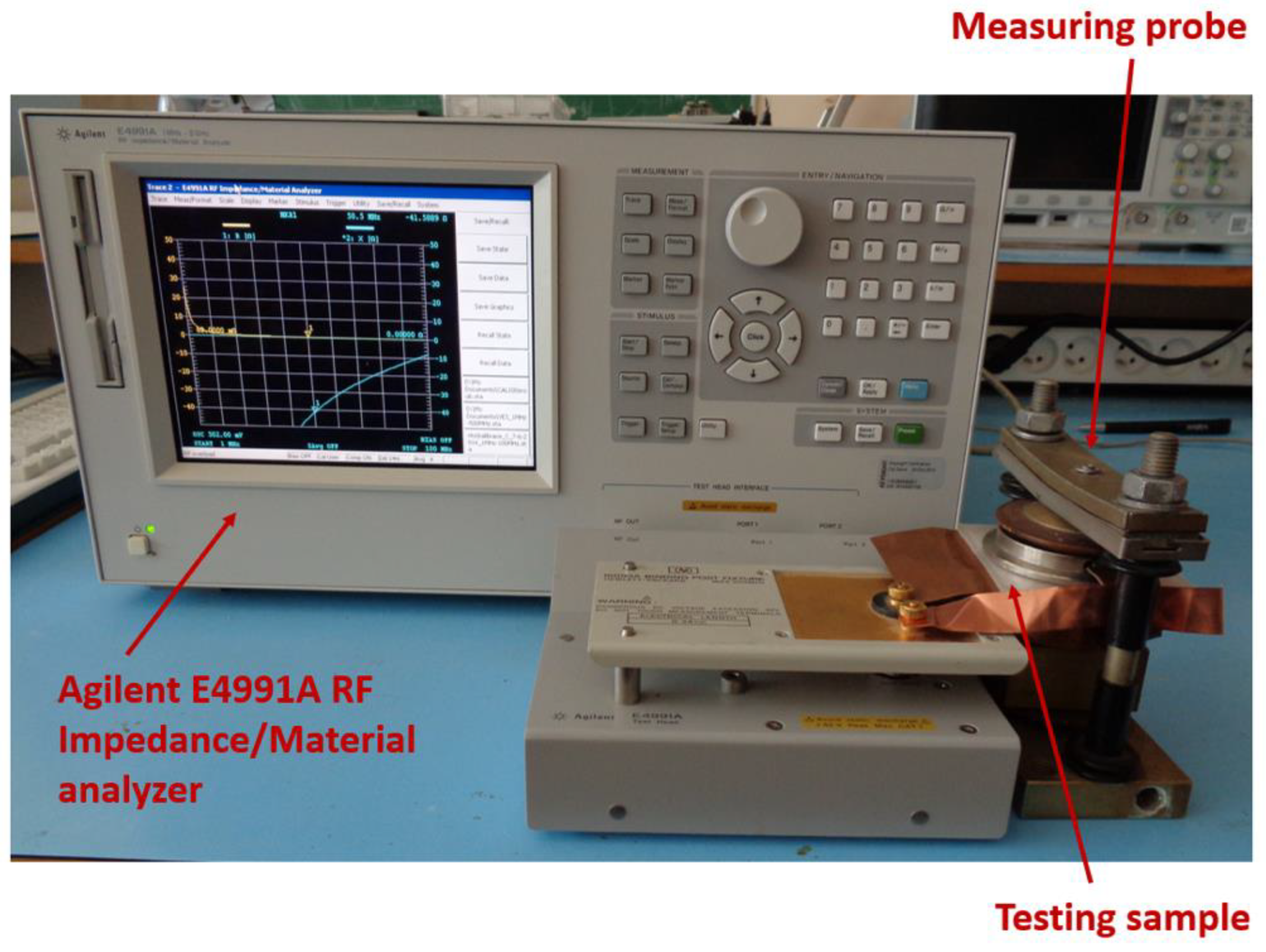
Figure 6.
Block diagram of measuring.
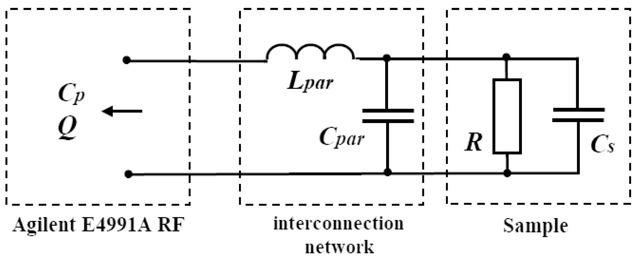
Figure 7.
Frequency dependence of relative permittivity (εr) of the colorless materials (PLA, ABS, PETG, and ASA).
Figure 7.
Frequency dependence of relative permittivity (εr) of the colorless materials (PLA, ABS, PETG, and ASA).

Figure 8.
Frequency dependence of relative permittivity (εr) of the PLA materials (PLA, PLA-Silver, and PLA-Metallic green).
Figure 8.
Frequency dependence of relative permittivity (εr) of the PLA materials (PLA, PLA-Silver, and PLA-Metallic green).
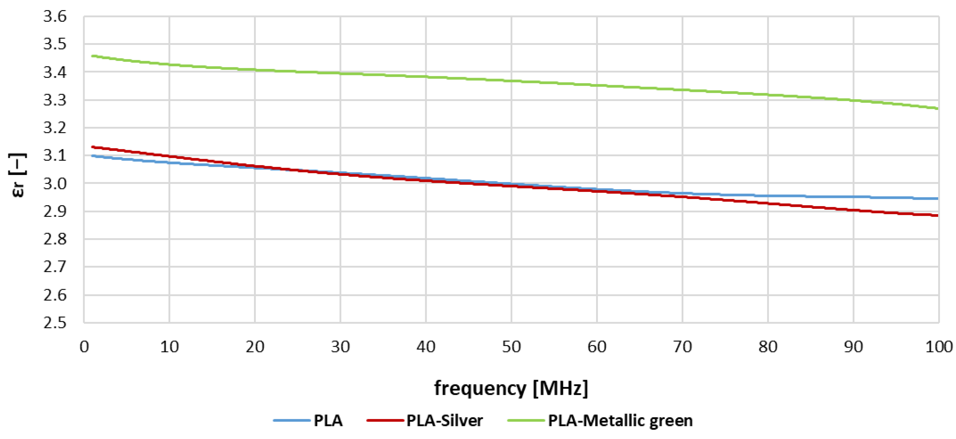
Figure 9.
Frequency dependence of the loss factor (tgδ) of the colorless materials (PLA, ABS, PETG, and ASA).
Figure 9.
Frequency dependence of the loss factor (tgδ) of the colorless materials (PLA, ABS, PETG, and ASA).
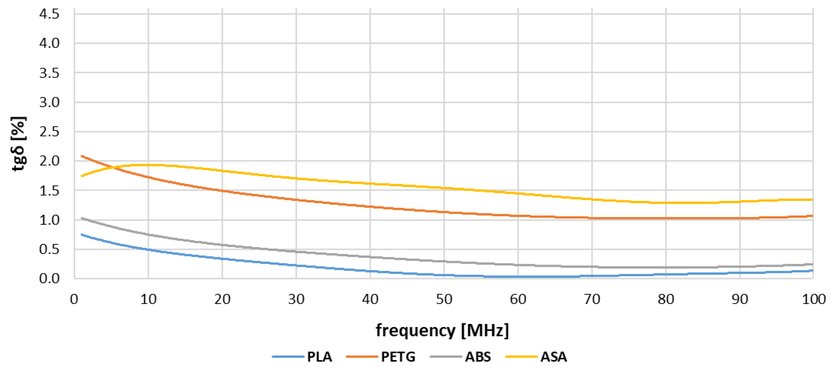
Figure 10.
Frequency dependence of the loss factor (tgδ) of the PLA materials (PLA, PLA-Silver, and PLA-Metallic green).
Figure 10.
Frequency dependence of the loss factor (tgδ) of the PLA materials (PLA, PLA-Silver, and PLA-Metallic green).
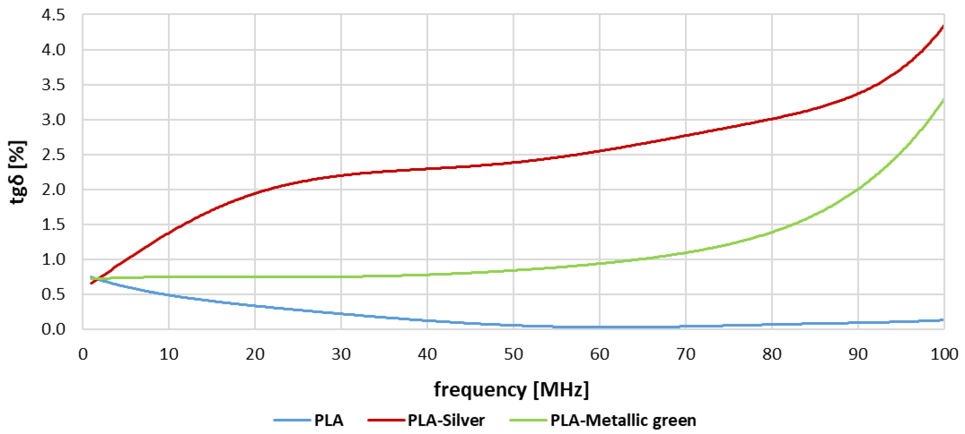
Figure 11.
Images of break surfaces of ABS, ASA, PETG, and PLA (colorless) taken with a microscope: (A) ABS—break surface, (B) ABS—grinded break surface, (C) ASA—break surface, (D) ASA—grinded break surface, (E) PETG—break surface, (F) PETG—grinded break surface, (G) PLA (colorless)—break surface, (H) PLA (colorless)—grinded break surface.


Table 1.
Samples’ properties and printing settings.
| Sample Identification | Material | Color | Printing Temperature [°C] 1st Layer/Subsequent Layers | Filament Manufacturer | Filament Diameter | |
|---|---|---|---|---|---|---|
| Hot end | Bed | |||||
| PLA | PLA | colorless | 215/210 | 60/60 | FilamentPM | 1.75 mm |
| PLA-Silver | silver | |||||
| PLA-Metallic green | metallic green | |||||
| PET-G | PET-G | colorless | 230/240 | 90/90 | ||
| ABS | ABS | 255/255 | 110/110 | |||
| ASA | ASA | 260/260 | 110/110 | |||
Table 2.
Statistical evaluation of the measured data of the relative permittivity (εr).
| Sample Identification | 1–100 MHz | |
|---|---|---|
| εr | ||
| aver. [-] 1 | st. dev. [-] 2 | |
| PLA | 3.00 | 0.05 |
| PLA-Silver | 2.99 | 0.07 |
| PLA-Metallic green | 3.36 | 0.05 |
| PETG | 3.30 | 0.05 |
| ABS | 2.95 | 0.04 |
| ASA | 3.19 | 0.06 |
1 aver. [-] means average value of the relative permittivity. 2 st.dev. [-] means standard deviation of the relative permittivity.
Table 3.
Statistical evaluation of the measured data of the loss factor (tgδ).
| Sample Identification | 1–19.9 MHz | 20–59.9 MHz | 60–100 MHz | |||
|---|---|---|---|---|---|---|
| tgδ | tgδ | tgδ | ||||
| aver. [%] 1 | st. dev. [%] 2 | aver. [%] 1 | st. dev. [%] 2 | aver. [%] 1 | st. dev. [%] 2 | |
| PLA | 0.51 | 0.12 | 0.15 | 0.09 | 0.07 | 0.03 |
| PLA-Silver | 1.38 | 0.43 | 2.28 | 0.15 | 3.13 | 0.45 |
| PLA-Metallic green | 0.75 | 0.08 | 0.80 | 0.07 | 1.63 | 0.65 |
| PETG | 1.74 | 0.17 | 1.24 | 0.12 | 1.04 | 0.03 |
| ABS | 0.77 | 0.13 | 0.38 | 0.10 | 0.21 | 0.02 |
| ASA | 1.88 | 0.05 | 1.62 | 0.11 | 1.34 | 0.06 |
1 aver. [%] means average value of the loss factor. 2 st.dev. [%] means standard deviation of the loss factor.
Publisher’s Note: MDPI stays neutral with regard to jurisdictional claims in published maps and institutional affiliations. |
© 2022 by the authors. Licensee MDPI, Basel, Switzerland. This article is an open access article distributed under the terms and conditions of the Creative Commons Attribution (CC BY) license (https://creativecommons.org/licenses/by/4.0/).
Share and Cite
MDPI and ACS Style
Picha, T.; Papezova, S.; Picha, S. Evaluation of Relative Permittivity and Loss Factor of 3D Printing Materials for Use in RF Electronic Applications. Processes 2022, 10, 1881. https://doi.org/10.3390/pr10091881
AMA Style
Picha T, Papezova S, Picha S. Evaluation of Relative Permittivity and Loss Factor of 3D Printing Materials for Use in RF Electronic Applications. Processes. 2022; 10(9):1881. https://doi.org/10.3390/pr10091881
Chicago/Turabian StylePicha, Tomas, Stanislava Papezova, and Stepan Picha. 2022. "Evaluation of Relative Permittivity and Loss Factor of 3D Printing Materials for Use in RF Electronic Applications" Processes 10, no. 9: 1881. https://doi.org/10.3390/pr10091881
Note that from the first issue of 2016, this journal uses article numbers instead of page numbers. See further details here.