Resistance-Capacitance Gas Sensor Based on Fractal Geometry
by
 , , ,
, , ,
Taicong Yang
1, 
Fengchun Tian
1,*,
James A. Covington
2,* ,
,
Feng Xu
1,
Yi Xu
3,
Anyan Jiang
1,
Junhui Qian
1,
Ran Liu
1,
Zichen Wang
4 and
Yangfan Huang
1 1
College of Communication Engineering, Chongqing University, 174 Sha Pingba, Chongqing 400044, China
2
School of Engineering, University of Warwick, Coventry CV4 7AL, UK
3
College of Optoelectronic Engineering, Chongqing University, 174 Sha Pingba, Chongqing 400044, China
4
Department of Mechanical Engineering, Carnegie Mellon University, Pittsburgh, PA 15213, USA
*
Authors to whom correspondence should be addressed.
Chemosensors 2019, 7(3), 31; https://doi.org/10.3390/chemosensors7030031
Submission received: 25 April 2019
/
Revised: 4 July 2019
/
Accepted: 8 July 2019
/
Published: 15 July 2019
(This article belongs to the Special Issue Advanced Electronic Noses and Chemical Detection Systems)
Abstract
:An important component of any chemiresistive gas sensor is the way in which the resistance of the sensing film is interrogated. The geometrical structure of an electrode can enhance the performance of a gas-sensing device and in particular the performance of sensing films with large surface areas, such as carbon nanotubes. In this study, we investigated the influence of geometrical structure on the performance of gas sensors, combining the characteristics of carbon nanotubes with a novel gas sensor electrode structure based on fractal geometry. The fabricated sensors were tested with exposure to nitric oxide, measuring both the sensor resistance and capacitance (RC) of the sensor responses. Experimental results showed that the sensors with fractal electrode structures had a superior performance over sensors with traditional geometrical structures. Moreover, the RC characteristics of these fractal sensors could be further improved by using different test frequencies that could aid in the identification and quantification of a target gas.

1. Introduction
Electronic noses (e-nose) are odor-recognizing instruments that consist of an array of gas sensors and pattern recognition algorithm. These do not attempt to identify individual chemicals but analyze the sample as a whole, allowing it to chemically sense complex odors that might be challenging when using other techniques. These instruments can be made cost-effective, tailored to a specific application and, where critical, can be of a non-invasive/non-destructive nature. They have been used in a broad range of applications, including medical diagnostics, food manufacture, industrial production, agriculture, and aerospace [1,2,3]. The gas sensor within the e-nose is one of the most critical components for sensing odors, which is a bottleneck for the sensitivity, precision, and response time of these instruments.
When the gas/odor molecule comes into contact with the sensitive material of the sensor, the gas molecules react chemically. Then the sensor converts the chemical signal into a form than can be detected as an electrical signal. Though there are a range of different gas/odor sensors, there are only a few companies which sell chemiresistive sensors that employ a spectrum of detection approaches. This is because many chemiresistive gas sensors do not respond well at low concentrations and have slow response times. Therefore, improving its sensitivity and speeding up the sensor response have become major research focuses [4,5]. A key factor affecting the performance of the sensor is the means of interrogating the sensing material. The influence of a specific surface area on sensitivity, is much greater than that of the material itself [6]. Therefore, increasing a specific surface area [7] and improving the structure of sensor are beneficial to improving the sensitivity of a sensor [8]. However, most studies had adopted traditional Euclidean geometry for sensor shape, with simple electrode structures that do not interrogate all of the sensing film and are typically formed of two parallel electrodes [9,10]. Later designs and the majority of MEMS (micro-electro-mechanical-systems) gas sensors that employ micro-hot plates, operated interdigitated fingers to try and increase the volume of the sensing film interrogated and reduce the measured resistance of the sensors [11]. However, with optimization, further improvements in the sensing film interrogation (and potentially sensitivity) could be achieved through more sophisticated electrode structures.
The term “fractal” was first proposed in 1975 by Benoit Mondelbrot. He was both a researcher at the Physics Department of the IBM Research Center (United States) and a Professor of Mathematics at Harvard University. For more than 30 years fractal theory has influenced various disciplines and have been applied in biology, geophysics, physics, chemistry, astronomy, materials science, and other fields. Many traditional scientific problems have been solved by the introduction of fractal theory. As a new concept and method, fractal is being applied and explored in many fields. The well-known American physicist Wheeler said: Who is not familiar with fractals in the future, who cannot be called a scientific cultural man [12].
Here, we report on the design of a new gas sensor structure based on fractal geometry. This sensor has a dual capacitance and resistance read out that are based on fractal geometry. The basic circuit model for this sensor has also been analyzed. Since carbon nanotubes (CNTs) are good gas sensing materials with a fast response-time, good repeatability, are able work at room temperature, have stable physical and chemical properties, and are easy to process in sensor manufacturing [13,14,15,16,17,18], we chose it to be the sensing material in our experiment, to verify the effectiveness of our sensor structure.
2. Fractal Electrode Design
In the field of geometry, fractal breaks the barrier of traditional Euclidean geometry. When it comes to a dimension, we always intuitively think of a line or a curve as a typical one-dimensional object and a plane as a typical two-dimensional object. Studies by Giuseppe Peano (1858–1932) [19] and David Hilbert (1862–1943) [20] have shown that a line segment can also be two-dimensional and can fill the entire plane; as illustrated in Figure 1.
This Hilbert curve, which is based on fractal geometry theory, provides new ideas for the design and manufacture of high performance gas sensors, due to its special structure and dimensions, compared to conventional Euclidean geometry. For capacitive gas sensors, the special fractal dimension provides a theoretical basis for the manufacture of ultra-large capacitors [21]. On the one hand, electric field lines between the two plates of the capacitor (shown in Figure 2a), represent the charge density and as the insulating layer in the middle of the parallel plate of Euclidean capacitor is narrow, the insulating layer is easily broken down when the electric field is strong, therefore, microelectronic measurement cannot be performed well. On the other hand, there also exists electric field penetration in the lateral space between the same side plates (shown in Figure 2b). If the parallel plates are paired laterally, they will store more energy and will produce a bigger capacitance.
Here, the capacitor plate was designed on a fractal structure, as shown in Figure 3. With this design, the special interlocking edge can withstand a larger electric field and generate a larger capacitance. Whilst the flux of the transverse electric field depends on the edge length of the plate, the design of the fractal plate can greatly increase the length of the plate under the same area, thereby resulting in the increase of the electric field strength and capacitance. The area occupied by the capacitor plates under different fractal orders control is the same, as the number of fractal orders gets larger, the ratio of plate length to the occupied area gets bigger, as shown in Figure 4 [21]. Hirad Samavati and his coworkers showed that with a horizontal spacing of 0.6 μm, a physical (not simulated) fabricated fractal plate with boundary dimension of about 1.6 has over twice the capacitance of a Euclidean capacitor of the same area. Simulations show that an increase of the boundary dimension of 1.80 would give a capacitance five times that of the Euclidean capacitor [21]. As the capacitance increases, changes in gas concentration can result in larger sensor responses, which in turn increases sensor sensitivity.
The parasitic capacitance of the sensor refers to the parasitic/stray capacitance between the plate and the substrate. It not only changes the capacitance value of the sensor, but also causes the sensor characteristics to be unstable, which can cause serious interference as the sensor itself has a small capacitance and the parasitic capacitance is extremely unstable. Especially when gas concentration rapidly changes, the influence of parasitic capacitance is large and cannot be ignored. The irregularity and randomness of the fractal capacitor electrode will help to reduce the influence of electric field strength and parasitic resonance and improve the stability of capacitive response [22].
3. Methods
3.1. Fractal Electrode Manufacture
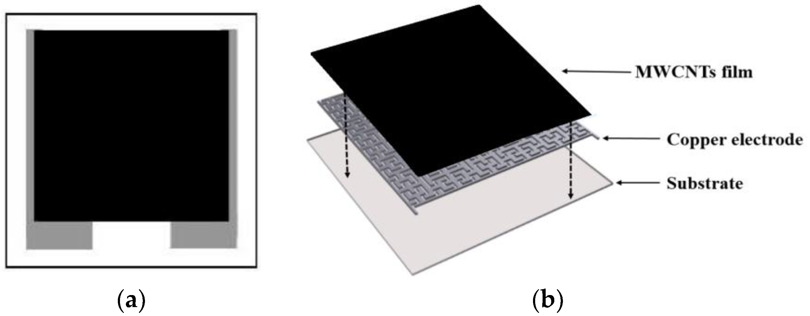
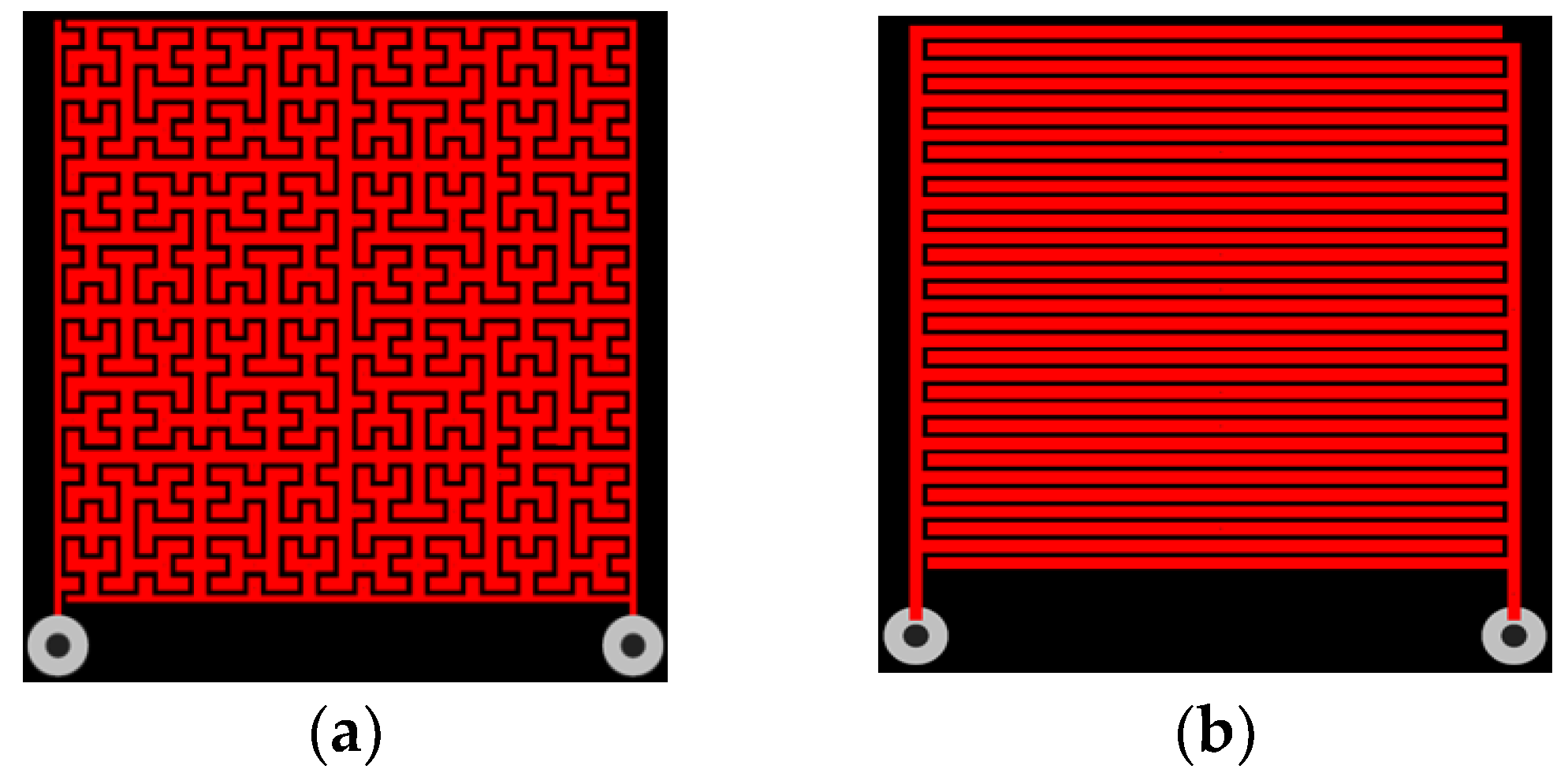
For comparison, both a traditional interdigitated electrode gas sensor and a fractal electrode gas sensor were designed simultaneously. Since conventional processing methods cannot satisfy the requirements of finger pitch and finger width of electrodes as required here (in the order of micrometers), microelectromechanical system (MEMS) processing was used to fabricate the sensor electrode. A copper clad plate was selected as substrate, which is not only insulated from the outside, but also has good adhesion to the electrodes and was convenient for dicing in mass production. The copper layer, with a specified thickness, was first electroplated onto the substrate, then etched into the electrode structure by a chemical reaction method. Finally, a thin layer of gold was deposited onto the surface of the electrode by a gold deposition process (pre-treatment, nickel deposition, gold deposition and post-treatment) to increase conductivity and prevent oxidation. The structure of each layer of the sensor is shown in Figure 5 [23]. The aspect ratio and effective areas of the fractal electrode and the interdigital electrode was 1:1. The electrode structure is shown in Figure 6, wherein the width of the plate is 400 μm, the pitch is 200 μm, and the thickness is 30 μm.
3.2. Carbon Nano Tube Coatings
To investigate the novel fractal electrode structure, we selected carboxylated multi-walled carbon nanotubes, produced by Chengdu Organic Chemicals Co., Ltd. (Chengdu, China China), Chinese Academy of Sciences, as the basic building material. This was selected as our group were experienced with depositing such films. It was prepared by catalytic cracking of natural gas through a nickel catalyst to obtain multi-walled carbon nanotubes, which were then prepared by oxidation of KMnO4 in H2SO4 solution. The main performance parameters are shown in Table 1 [24].
We adopted a combination of a drop coating and a spin coating method to prepare a translucent conductive carbon nanotube film under optimized process parameters. CNTs were first dispersed is a combination of a dispersant (TNWDIS, Carbon nanotube water dispersant, Chengdu Organic Chemicals Co., Ltd., Chinese Academy of Sciences) and deionized water, which was followed by an ultrasonic treatment. This was proceeded by a centrifuged treatment to remove undispersed particles. The electrode plates were cleaned in ethanol and washer in deionized water before deposition. Then a small amount of dispersed CNTs were dropped onto the electrodes whilst it was spun to form a control layer thickness. The resistance of the film was continuously measured to ensure each coating was of a similar thickness.
3.3. Sensor Measurement
To measure the response of the gas sensor, it was connected in series with fixed resistor, as shown in Figure 7. Here an AC (alternating current) sine wave signal generated by VirtualBench virtual instrument (National Instrument, USA) was used as the input signal and the voltage V1 across the sensor was detected by data acquisition card (DAQ, ART Technology, China). The impedance characteristics of the sensor was proportional to the input the voltage V1 sensor. Thus, if we define the impedance of sensor to be Z, and the voltage of the signal source be U, we have:
After absorbing gases, the impedance of the sensor changes, wherein the voltage change across the sensor, in the circuit, was measured and corresponding gas concentration was obtained by calculation. Under test, the sensors were exposed to 3 min of dry clean air, followed by an injection of the target gas (nitric oxide in this case) for a further 3 min. Different concentrations of NO gas were used in the tests from 2 to 10 ppm. The air chamber was a 325 ml stainless steel box coated with Teflon. Sensors were welded on a printed circuit board (PCB) and placed upside down in the box. All sensors operated at room temperature. A mass flow controller (MFC) was used to control gas flow rate. The test system is shown in Figure 8.
The sensor response is defined as:
where V represent sensor response at current concentration, V0 represent sensor response at 0 ppm of stimulus.
4. Results and Discussion
4.1. Morphology
The SEM (scanning electron microscopy) image of the MWNTs (Multi-walled carbon nanotubes) film obtained is shown in Figure 9. Image at the top left is enlarged to a scale of 500 μm, which shows that the carbon nanotubes were uniformly deposited in gaps between the fractal electrodes. The image at the right was enlarged to a scale of 20 μm, from which a stacked pattern of multi-walled carbon nanotubes and spaces between nanotubes can be seen. The detected gas was capable of being adsorbed in these spaces, resulting in physical or chemical changes, thereby changing the electrical conductivity or dielectric constant of the carbon nanotubes as a medium.
In order to further detect the thickness between the sensor electrode and the film, a Veeco Dekak 150 surface probe profilometer manufactured by Bruker Veeco was used to test the surface thickness and roughness of the sensor film. The test result indicated that the deposited MWCNT film had a thickness of between 24–27 μm.
4.2. Gas Sensing Characteristic
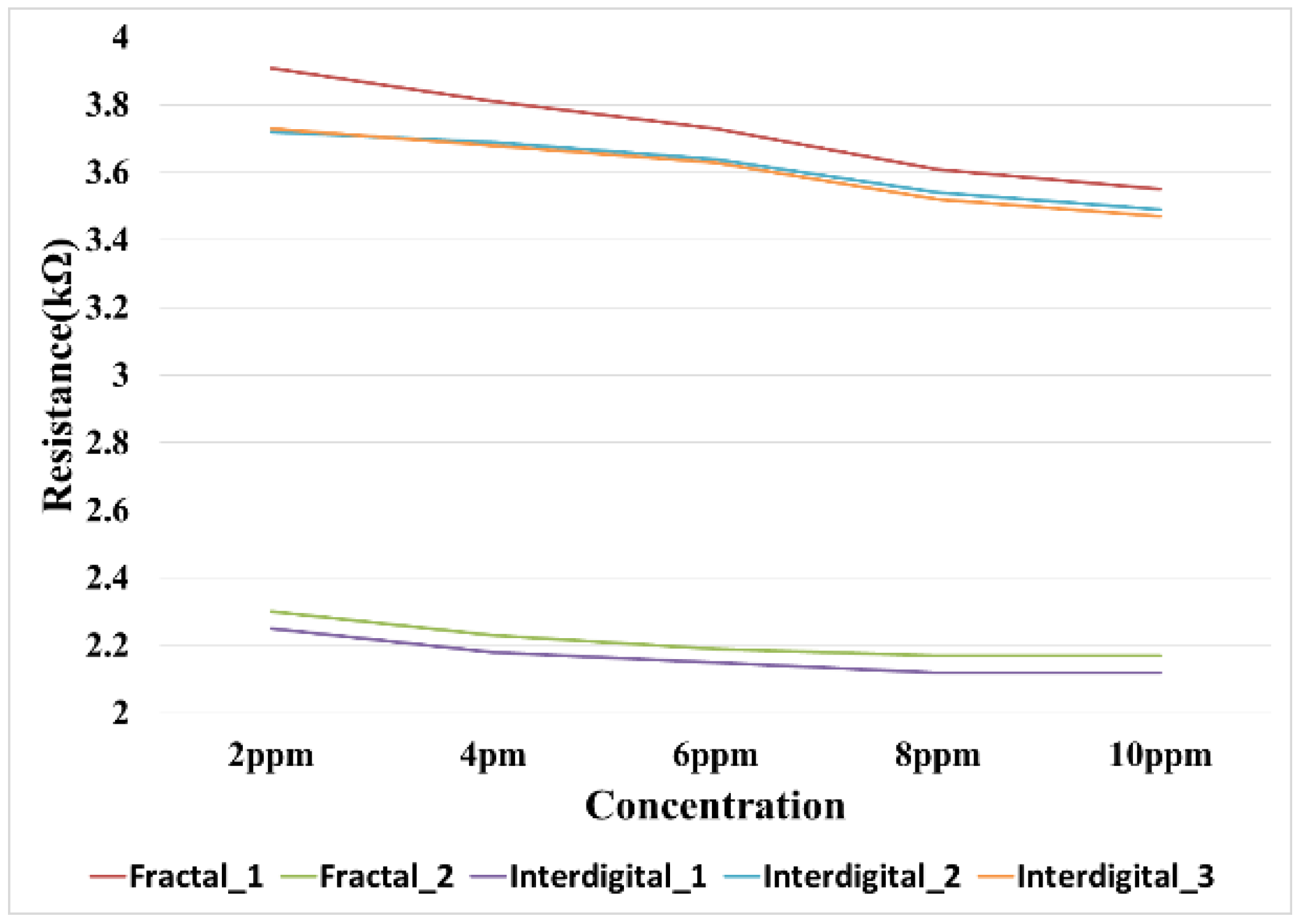
In order to verify the repeatability of the sensor, we manufactured two sensors with fractal electrodes and three with interdigital electrodes. To test the basic functionality of the sensor (before AC measurements), we measured the resistance across the sensor using a simple multimeter (VICTOR, China) and exposed the sensor to 2–10 ppm of NO in 2 ppm steps. The obtained resistances are shown in Figure 10. As can be seen the resistance of all the sensors changed in a similar way, as the gas concentration increased. However, their initial resistance values (resistance of sensor under clean air) were different, which is due to the discrepancy of the MWCNTs film in the coating process.
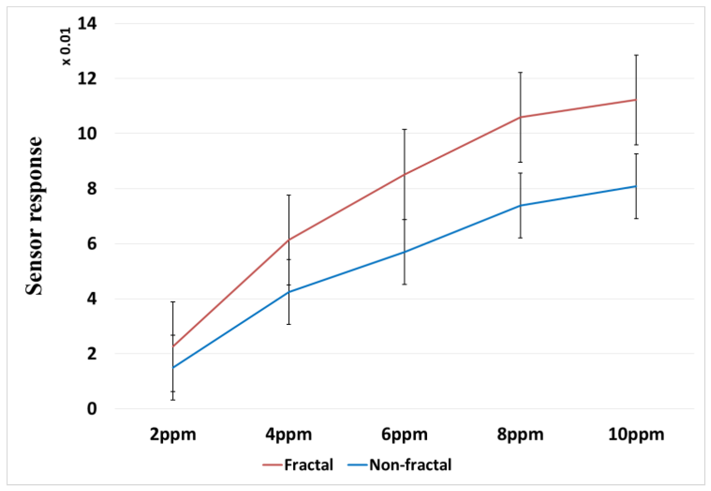
The change in sensitivity of the sensor with NO concentration is shown in Figure 11 below. Here we see the gas response following a traditional power law model.
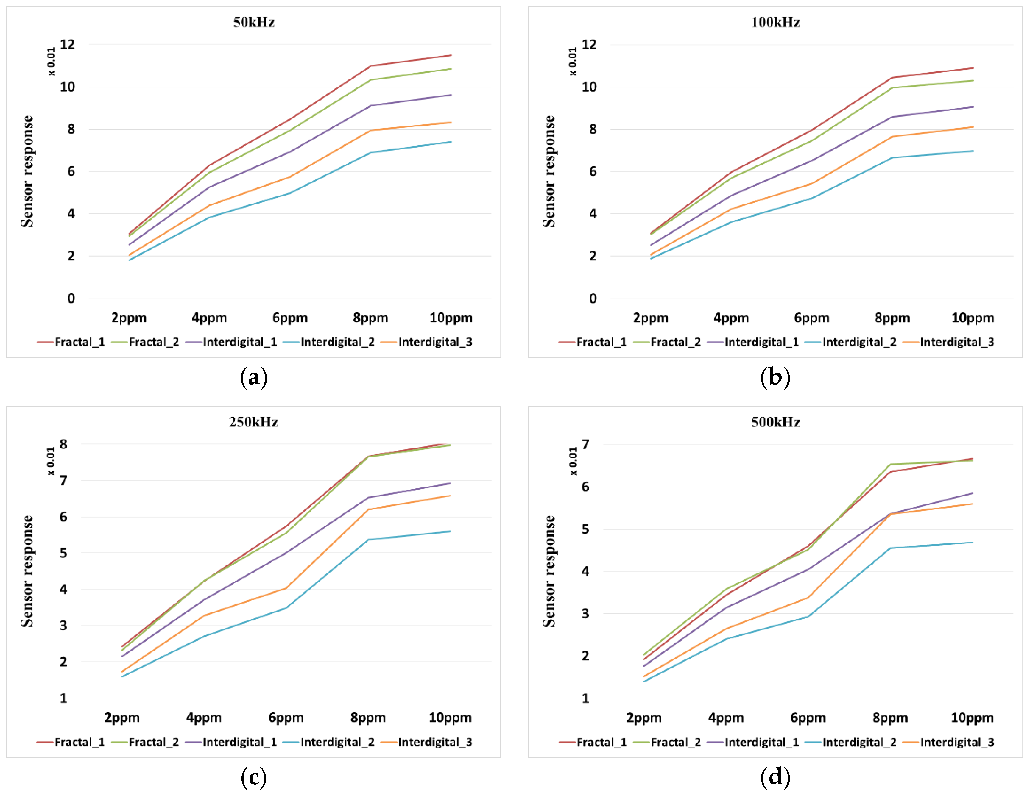
From the initial DC measurements, we were able to confirm that our sensors responded to NO across the required concentration range. Thus, we then considered the impedance of the sensors at four different frequencies (50, 100, 250 and 500 kHz). These were chosen to give a broad spectrum of different impendence values. The sensors were then tested to the same NO concentrations used earlier. The results of these measurements are shown in Figure 12.
As it can be seen from Figure 12, the response amplitude of the fractal electrode sensor was greater than of the interdigital electrode sensor under the same conditions. Thus, it shows that the fractal electrode gas sensor outperformed, in terms of sensitivity, those formed from traditional electrode geometries. Evaluating only the fractal sensors, we then considered the sensitivity and a function of frequency over the NO gas range defined earlier. The results of this are shown in Figure 13 below.
This figure shows that the higher the NO concentration, the greater the difference of sensor response at different frequencies. Moreover, the response amplitude was large at low frequencies, while the linearity of the response curve was not so good. These characteristics need more investigation in subsequent experiments. Depending on the concentration of the gas being measured, the frequency of signal source can be adjusted to optimize the response of sensor, which helps to extend the range of concentration detection. At the same time, for different types of gases to be tested, adjusting the sensor response at different frequencies may improve features among different types of gases, which helps the sensor to distinguish gas species.
5. Conclusions
In this paper, the influence of the shape structure of a sensor on its gas-sensitive characteristics was studied. The fractal theory was introduced into the structure design of resistance and capacitance (RC)-based gas sensors. The structure of the film on the surface of the sensor was examined by physical methods such as scanning electron microscopy and a surface probe profilometer. With NO as test gas, the effectiveness of the sensor was proved by experiments. It is showed that the design method can effectively improve the sensitivity of gas sensor and provide a new method for the development of high performance gas sensors.
In our experiments, the sensors showed poor linearity. In the future, nanomaterials such as graphene or high molecular polymer may be considered as replacements. At the same time, electrodes of the sensor can be further miniaturized by means of a microelectromechanical system. Finally, in the future, the selectivity of the sensor can be further verified by detecting multiple gases.
Author Contributions
Conceptualization, F.T. and J.A.C.; data curation, T.Y., F.X.; formal analysis, F.T., T.Y.; funding acquisition, J.A.C., R.L.; investigation, A.J., Y.H.; methodology, T.Y., F.T., Y.X., J.Q.; project administration, F.T.; resources, Y.X., J.Q., R.L.; software, Y.H., T.Y.; supervision, F.T.; validation, F.X., R.L.; visualization, Z.W., R.L., J.Q.; writing–original draft preparation, T.Y.; writing—review and editing, J.A.C., Z.W.
Funding
This research was funded by the Common Crucial Technique Innovation Project of Chongqing Key Industries (cstc 2016zdcy-ztzx007-03), the National International Science and Technology Cooperation Project (2014DFA31560), and the Chongqing Research Program of Basic Research and Frontier Technology (No. cstc2016jcyjA0103).
Conflicts of Interest
The authors declare no conflicts of interest.
References
- Li, S.; Wang, W.; Liang, F.; Zhang, W.X. Heavy metal removal using nanoscale zero-valent iron (nZVI): Theory and application. J. Hazard. Mater. 2016, 322, 163–171. [Google Scholar] [CrossRef] [PubMed]
- Chen, X. Method for Improving Detection Accuracy of Electronic Nose System. Master’s Thesis, Chongqing University, Chongqing, China, 2016. [Google Scholar]
- Zhang, W. Research on Key Technologies of Gas Identification Based on Sensor Array Transient Response. Ph.D. Thesis, National University of Defense Technology, Changsha, China, 2013. [Google Scholar]
- Schroeder, V.; Savagatrup, S.; He, M.; Lin, S.; Swager, T.M. Carbon Nanotube Chemical Sensors. Chem. Rev. 2019, 119, 1599–1663. [Google Scholar] [CrossRef] [PubMed]
- Ishihara, S.; Labuta, J.; Nakanishi, T.; Tanaka, T.; Kataura, H. Amperometric Detection of Sub-ppm Formaldehyde Using Single-Walled Carbon Nanotubes and Hydroxylamines: A Referenced Chemiresistive System. ACS Sens. 2017, 2, 1405–1409. [Google Scholar] [CrossRef] [PubMed]
- Wang, X. Fabrication of Porous Metal Oxide Semiconductors and Analysis of Their Properties. Ph.D. Thesis, Shandong University, Jinan, China, 2014. [Google Scholar]
- Gillet, M.; Aguir, K.; Bendahan, M.; Mennini, P. Grain size effect in sputtered tungsten trioxide thin films on the sensitivity to ozone. Thin Solid Films 2005, 484, 358–363. [Google Scholar] [CrossRef]
- Xiao, C. Study on the One-Dimensional Structure Design of Nanomaterials and Their Gas Sensing Properties. Master’s. Thesis, Jilin University, Changchun, China, 2015. [Google Scholar]
- Bo, L. Study on Structure Improvement of Microstructured Si-based SnO2 Gas Sensor. Master’s Thesis, Dalian University of Technology, Dalian, China, 2010. [Google Scholar]
- Zhang, Q.; Guan, Z.-S. Gas Sensors of Electric Resistance Semiconductors. Instrum. Tech. Sens. 2006, 7, 6–9. [Google Scholar]
- Ma, X. Study on Design and Characteristics of Micro-Structure Gas Sensor Based on Silicon Substrate. Master’s Thesis, Jilin University, Changchun, China, 2013. [Google Scholar]
- Lin, X. Philosophical Random Walk in Fractals; Capital Normal University Press: Beijing, China, 1999. [Google Scholar]
- Iijima, S. Helical microtubules of graphitic carbon. Nature 1991, 354, 56–58. [Google Scholar] [CrossRef]
- Zhou, C.; Kong, J.; Dai, H. Electrical measurements of individual semiconducting single-walled carbon nanotubes of various diameters. Appl. Phys. Lett. 2000, 76, 1597–1599. [Google Scholar] [CrossRef]
- Hannon, A.; Lu, Y.; Li, J.; Meyyappan, M. Room temperature carbon nanotube based sensor for carbon monoxide detection. J. Sens. Sens. Syst. 2014, 3, 349–354. [Google Scholar] [CrossRef]
- Kong, J.; Franklin, N.R.; Zhou, C.; Chapline, M.G.; Peng, S.; Cho, K.; Dai, H. Nanotube molecular wires as chemical sensors. Science 2000, 287, 622–625. [Google Scholar] [CrossRef] [PubMed]
- Li, J.; Lu, Y.; Ye, Q.; Cinke, M.; Han, J.; Meyyappan, M. Carbon Nanotube Sensors for Gas and Organic Vapor Detection. Nano Lett. 2003, 3, 929–933. [Google Scholar] [CrossRef]
- Hoa, N.D.; Quy, N.V.; Cho, Y.; Kim, D. An ammonia gas sensor based on non-catalytically synthesized carbon nanotubes on an anodic aluminum oxide template. Sens. Actuators B Chem. 2007, 127, 447–454. [Google Scholar] [CrossRef]
- Peano, G. Sur une courbe, qui remplit toute une aire plane. Math. Ann. 1970, 36, 157–160. [Google Scholar] [CrossRef]
- Hilbert, D. Über die stetige Abbildung einer Linie auf ein Flächenstück. Math. Ann. 1891, 38, 459–460. [Google Scholar] [CrossRef]
- Frame, M.; Urry, A. Fractal Worlds: Grown, Built, and Imagined; Yale University Press: New Haven, CT, USA, 2016. [Google Scholar]
- Xu, W.; Zhuang, M.; Wang, D. Fractal Planar Capacitors Based on Interdigital Structures. J. Jimei Univ. Nat. Sci. 2010, 15, 389–393. [Google Scholar]
- Deng, H. Research of the MWNTs Benzene Series Vapor Sensor. Master’s Thesis, Harbin Institute of Technology, Harbin, China, 2010. [Google Scholar]
- Chengdu Organic Chemicals Co., Ltd. Chinese Academy of Sciences. Multi-Walled Carbon Nanotube Material Technical Data [EB/OL]. Available online: http://meizhenqu.l58a.bolead.com/view.php?prt=3,29,50,81&id=114 (accessed on 6 May 2019).
Figure 1.
Space-filling curve explored by Hilbert (First six steps/orders shown).

Figure 2.
Illustration of the electrical field between capacitor plates.

Figure 3.
Schematic of a fractal capacitor.

Figure 4.
Ratio of plate length versus area under different fractal orders.

Figure 5.
Illustration of sensor structure. (a) Top view; (b) side view.

Figure 6.
Structure diagram of sensor plate. (a) Fractal electrode; (b) ordinary Euclidean electrode (interdigital electrode).
Figure 6.
Structure diagram of sensor plate. (a) Fractal electrode; (b) ordinary Euclidean electrode (interdigital electrode).

Figure 7.
Experimental circuit.

Figure 8.
Gas sensing test system.

Figure 9.
SEM images of multi-walled carbon nanotube films at different magnifications (scale bars, left: 1 mm; right: 20 μm).
Figure 9.
SEM images of multi-walled carbon nanotube films at different magnifications (scale bars, left: 1 mm; right: 20 μm).

Figure 10.
Resistance versus concentration curves of the five sensors.

Figure 11.
Curve of sensor responses to NO with standard error bars at concentration gradient.

Figure 12.
Comparison of sensor responses between the two structures. (a) Response at 50 kHz; (b) response at 100 kHz; (c) response at 250 kHz; (d) response at 500 kHz.
Figure 12.
Comparison of sensor responses between the two structures. (a) Response at 50 kHz; (b) response at 100 kHz; (c) response at 250 kHz; (d) response at 500 kHz.

Figure 13.
Response of the fractal sensor to NO gases at different frequencies.


Table 1.
Performance parameters of carboxylated multi-walled carbon nanotubes.
| Characteristic | Unit | MWCNTs | Characterization Method |
|---|---|---|---|
| Outer Diameter | nm | 20–30 | HRTEM (high resolution transmission electron microscope), Raman |
| Purity | wt% | >98 | TGA (thermal gravimetric analyzer) & TEM (transmission electron microscope) |
| Length | μm | 10–30 | TEM |
| Special Surface Area | m2/g | >110 | BET (Brunauer, Emmett, Teller) Specific Surface Area Detection Method |
| ASH | wt% | <1.5 | TGA |
| Electric Conductivity | s/cm | >100 | - |
| Tap Density | g/cm3 | 0.28 | - |
| -COOH Content | wt% | 1.23 | XPS (X-ray photoelectron spectroscopy) & Titration |
© 2019 by the authors. Licensee MDPI, Basel, Switzerland. This article is an open access article distributed under the terms and conditions of the Creative Commons Attribution (CC BY) license (http://creativecommons.org/licenses/by/4.0/).
Share and Cite
MDPI and ACS Style
Yang, T.; Tian, F.; Covington, J.A.; Xu, F.; Xu, Y.; Jiang, A.; Qian, J.; Liu, R.; Wang, Z.; Huang, Y. Resistance-Capacitance Gas Sensor Based on Fractal Geometry. Chemosensors 2019, 7, 31. https://doi.org/10.3390/chemosensors7030031
AMA Style
Yang T, Tian F, Covington JA, Xu F, Xu Y, Jiang A, Qian J, Liu R, Wang Z, Huang Y. Resistance-Capacitance Gas Sensor Based on Fractal Geometry. Chemosensors. 2019; 7(3):31. https://doi.org/10.3390/chemosensors7030031
Chicago/Turabian StyleYang, Taicong, Fengchun Tian, James A. Covington, Feng Xu, Yi Xu, Anyan Jiang, Junhui Qian, Ran Liu, Zichen Wang, and Yangfan Huang. 2019. "Resistance-Capacitance Gas Sensor Based on Fractal Geometry" Chemosensors 7, no. 3: 31. https://doi.org/10.3390/chemosensors7030031
Note that from the first issue of 2016, this journal uses article numbers instead of page numbers. See further details here.