Review

Chemical Vapour Deposition of Gas Sensitive Metal Oxides

1
SIX Research Centre, Brno University of Technology, Technická 10, Brno, CZ-61600, Czech Republic
2
Department of Chemistry, University College London, 20 Gordon Street, London, WC1H 0AJ, UK
3
Material Science and Nanotechnology Lab, Department of Physics, GC University Lahore, Pakistan
*
Author to whom correspondence should be addressed.
Chemosensors 2016, 4(1), 4; https://doi.org/10.3390/chemosensors4010004
Submission received: 17 November 2015 / Revised: 26 January 2016 / Accepted: 5 February 2016 / Published: 1 March 2016
(This article belongs to the Special Issue Chemical Vapor Sensing)

Abstract

:
This article presents a review of recent research efforts and developments for the fabrication of metal-oxide gas sensors using chemical vapour deposition (CVD), presenting its potential advantages as a materials synthesis technique for gas sensors along with a discussion of their sensing performance. Thin films typically have poorer gas sensing performance compared to traditional screen printed equivalents, attributed to reduced porosity, but the ability to integrate materials directly with the sensor platform provides important process benefits compared to competing synthetic techniques. We conclude that these advantages are likely to drive increased interest in the use of CVD for gas sensor materials over the next decade, whilst the ability to manipulate deposition conditions to alter microstructure can help mitigate the potentially reduced performance in thin films, hence the current prospects for use of CVD in this field look excellent.

Graphical Abstract

1. Introduction

Gas detection, and determining the composition of gas mixtures, is necessary in many different fields, for example environmental monitoring, vehicle and industrial emission control and household security. Most studies have focused on the detection of H2, CO2, CO, O2, O3 or NH3, because of their toxicity, their relation with atmospheric composition or the fact that they can be found at high levels in some environments. Detection of organic vapors such as methanol, ethanol, isopropanol, benzene and amines are also of great interest [1]. Metal oxides were some of the first materials used in chemoresistive gas sensors and are still the most widely used gas sensing materials. Numerous metal oxide semiconductor materials, including both single (e.g., ZnO, SnO2, WO3, TiO2 and Fe2O3) and multi-component (BiFeO3, MgAl2O4, SrTiO3, and Sr1- yCayFeO3-x) oxides, have been reported for use as the active layer [2,3]. The mechanism for gas detection in these materials is based on reactions that occur at the sensor surface, resulting in a change in the concentration of adsorbed oxygen. Oxygen ions adsorb onto the material’s surface, removing electrons from the bulk and creating a potential barrier that limits electron movement and conductivity. When reactive gases combine with this oxygen the height of the barrier is altered, changing conductivity. This change in conductivity is directly related to the composition of the gaseous environment allowing a quantitative determination of the gases present (under certain conditions) [4]. Metal oxide semiconductor sensors have proved to be sensitive to a large range of gases and studies have focused on understanding the relationship between sensor response and materials processing and chemistry, e.g., dopant level, synthesis and annealing temperature. These parameters can have a profound effect on the materials chemistry and structure, which in turn dramatically affect the gas sensing properties of the sensor device [2]. Currently the potential of metal oxide semiconductor sensors has not been fully realised, with other types of sensors (e.g., electrochemical or those based on optical or photo-ionisation principles) still favored for many industrial applications. However, new materials and techniques continue to be developed to improve the abilities and properties of metal oxide gas sensors, and with recent advances in understanding of materials chemistry and synthetic techniques their intrinsically favourable properties, coupled with their relative low cost and potential for miniaturization and portability, should mean they become ever more important tools in environmental monitoring.
Development of synthetic methods for producing materials for use in metal oxide gas sensors has been a major focus in the field and many routes have been investigated including hydrothermal [5], sol-gel [6], solid-state chemical reaction [7], thermal evaporation [8], vapor-phase transport [9], RF sputtering [10] and molecular beam epitaxy [11]. Two common preparative routes are solid-state and sol-gel; solid-state reactions allow for relatively simple synthesis but for complex materials can lead to poor chemical homogeneity, whilst sol-gel reactions provide very good homogeneity and small particle size dispersion but the process can be difficult to control reproducibly. An alternative synthesis technique is chemical vapour deposition (CVD), which is a process for the deposition of films of various materials via chemical reactions of gaseous reactants in an activated environment (e.g., temperature, light or plasma). In general, a CVD system consists of three main components:
  • Precursor supply system
  • CVD reactor
  • Exhaust system.
The role of the precursor supply system is to generate precursors in the vapour phase and deliver them to the reactor, normally with the help of carrier gas, where the CVD reaction takes place. Typically, liquid precursors are used in order to generate sufficient vapour pressure when heated to intermediate temperature (<200 °C) with mixing of multiple precursor streams used to produce complex mixtures. Variants on this system such as liquid injection- and aerosol assisted-(AA)CVD [12] are typically used to introduce low volatility/solid precursors, with precursor evaporation only occurring inside the CVD reactor, although they also afford great opportunities in synthesizing doped or ternary/quaternary materials due to the relative ease of controlling stoichiometry through the precursor solution.
The reactor is where external energy is added to the system, in the form of heat, light or plasma, to initiate the deposition reaction(s). Deposition involves two principal types of reactions, homogenous and heterogeneous; homogeneous reactions occur exclusively in the gas phase whilst heterogeneous reactions occur between gas phase species and a solid substrate (although frequently involving an initial gas phase reaction resulting in the formation of reactive intermediate species). In the case of homogeneous reaction the precursor/intermediate species undergo further gas phase decomposition resulting in the formation of a powder and by-products. This powder is typically non-adherent and these reactions are undesirable in CVD (although in pyrolysis reactions the powder may be the target and collected via a powder capture system), whilst the by-products are removed from the reaction chamber through the exhaust system. In the case of heterogeneous reactions diffusion of the precursor/intermediate species occurs at an interfacial gas/solid boundary layer, forming nucleation sites on the solid substrate. Subsequent nucleation processes take place on the surface of substrate resulting in the deposition of solid material, and manipulation of the reaction conditions can be used to promote the formation of either planar films or nanostructures [13]. It is also worth noting that the nature of the heterogeneous reactions means that the materials are atomically mixed, and under well-controlled conditions are homogeneous in composition across the deposition area. Hence CVD offers several potential advantages over other synthesis processes for the preparation of gas sensing materials and sensors, which include:
  • A single step for gas sensor processing which combines both materials synthesis and integration of the material with the sensor platform.
  • Production of atomically mixed homogenous materials, including complex stoichiometries, with good reproducibility.
  • Ability to influence crystal structure and surface morphology.
This article presents a review of recent research efforts and developments for the fabrication of metal-oxide gas sensors using chemical vapour deposition (CVD), presenting its potential advantages as a materials synthesis technique for gas sensors along with a discussion of their sensing performance. In considering the literature we have compiled tables of sensing data, however we note that these are only a qualitative comparison as the response of metal oxide semiconductors in general is dependent not only on the material properties but also on the conditions used to test these materials towards the analytes.

2. Gas Sensing Materials

2.1. Tungsten Oxide

Tungsten oxide, WO3, is a wide-bandgap n-type semiconductor, with bandgaps reported in the range of approximately 2.6–3.2 eV dependent on crystallinity and oxygen deficiency. WO3 crystals are generally formed by corner and edge sharing of WO6 octahedra, with various crystal phases dependent on temperature; monoclinic II (ε-WO3, < −43 °C) → triclinic (δ-WO3, −43 ° C to 17 °C) → monoclinic I (γ-WO3, 17 °C to 330 °C) → orthorhombic (β-WO3, 330 ° C to 740 °C) → tetragonal (α-WO3, > 740 °C). Tungsten oxide can also possess non-stoichiometric properties because its rhenium oxide-like lattice can withstand a considerable amount of oxygen deficiency. Some of the better known non-stoichiometric tungsten oxides are W20O58, W18O49 and W24O68 [14].
Vapour deposited WO3 and WOx have both been used for gas sensing. These materials are typically monoclinic or tetragonal phases with a variety of morphologies reported including films, particles and low dimensional structures, with the formation of nanostructures (NS) demonstrated below 600 °C for AACVD [15] and at 800 °C for hot filament CVD. The starting materials reported in the production of gas sensitive tungsten oxide include metallic W [16,17], WO3 (powder, pellet) [18,19], WCl6 [20], W(OCl4) [21], W(CO)6 [22,23,24], or complexes such as [W(OPh)6] [25,26], [NH4][W12O39], [NH4]10H2[W2O7]6 or [nBu4N]2[W10O32] [27]. Most commonly planar films of vapour deposited tungsten oxide have been employed and integrated directly into ceramic- [20,21,26,27], silicon- [16,22,23,25] or polymer-based [28] gas sensing devices. The localized CVD of tungsten oxide nanostructures on Si-based microhotplates (Figure 1) via heating provided from the sensor platform itself, rather than from the reactor chamber, has also been demonstrated as a viable method for the fabrication of gas sensors based on tungsten oxide [23], which provides interesting new possibilities for sensor processing.
As with other metal oxides, tungsten oxide deposited via CVD has been used in resistive mode, with demonstrated sensitivity to NO2 [16,21,26], N2O [17], C2H5OH [20,27], CO [23,25], NH3 [18], H2 [22], humidity [19] and aromatic compounds such as benzene [29] and toluene [30] (Table 1). The relative sensor response (R) to ppm concentrations (C) of CO, C2H5OH and NO2 (Table 1) are plotted in Figure 2. This relative value (i.e., Response/Concentration) was used as a quantitative factor to compare the sensitivity of the most common CVD-deposited tungsten oxide morphologies reported in the literature, although it is worth noting that strictly sensitivity is defined as the slope of the calibration curve (calibration curves were not available in most of the reports summarized in Table 1). It is apparent from Figure 2 that tungsten oxide has a notable sensitivity to NO2 and this characteristic is generally observed for tungsten oxide making it a good candidate to selectively detect NO2 in the presence of gases such as C2H5OH, CH4, CO, NH3, H2, C6H6 and H2S [21,24].
The properties of CVD have been used to enhance the performance of thin film tungsten oxide-based resistive sensors in several ways. For instance, the sensing properties to ethanol were improved by a change in microstructure that occurred by controlling film thickness in the range 6700 nm to 3600 nm. These changes produced a reduction in the baseline resistance of the sensors, with resistance decreasing with decreasing film thickness, with an attendant modification of the activation energy of conductance [20]. We note a similar study has demonstrated improved sensor performance in thicker films (30,000 nm) compared to thinner films (15,000 nm) [27], but it is likely that these results are influenced by the properties of the electrodes, specifically the electrode thickness, which need to have a similar thickness to that of the thin film sensor material in order to achieve optimum sensor performance [31]. For NP tungsten oxide, CVD has been used to control the size of NPs to improve sensor performance, with particles with sizes below 100 nm having better sensing properties to NO2 regardless of processing parameters such as the oxygen pressure during CVD or the subsequent annealing temperature. This was attributed to the depletion layer extending throughout the material in small particles hence providing a larger conductivity change than for large particles that which are depleted only at the surface [16]. In addition, by manipulating CVD conditions to favour formation of networked nanowire mats rather than NPs the sensitivity of tungsten oxide to N2O was improved by an order of magnitude compared to NP films (Figure 3). This was related to the higher surface-to-volume ratio of NS compared to NPs, although this study also highlights the need to use highly networked nanowires as opposed to (quasi) aligned nanowires for optimum gas sensing performance, as these behave similarly to single nanowire or parallel nanowire arrays [17]. Similar observations were also reported for gas microsensors based on tungsten oxide nanoparticles and nanowires grown via AACVD (Figure 3) [32].
CVD has also been demonstrated to simplify sensor processing by providing direct integration of tungsten oxide sensor materials with the sensor platform. This has been demonstrated particularly for aerosol assisted CVD, which has shown the selective deposition of networked or quasi-aligned tungsten oxide NS on ceramic- [33], silicon- [32] and polymer-based platforms [28].

2.2. Zinc Oxide

Zinc oxide (ZnO) is a II-VI semiconductor with a wide direct band gap (3.37 eV), large exciton binding energy (60 meV), spontaneous polarization and piezoelectric constants which make it an attractive material for electronic, optoelectronic, energy generator and photocatalytic applications [34]. This material has been widely used for gas detection since the early 1960s, and it is still among the most reported metal oxide materials used for gas sensing. Most of the interesting functionalities of ZnO originate from its wurtzite crystal structure, which can be described as a number of alternating planes composed of tetrahedrally coordinated O2− and Zn2+ ions, stacked along the c-axis. This crystal does not possess inversion symmetry, having a large spontaneous polarization along the [0001] crystalline direction [34,35].
Metallic Zn [36,37,38,39,40,41,42,43] or diethylzinc (Et2Zn) [44,45,46,47], both with O2 as carrier (reactive) gas, have been used as precursors for the formation of ZnO via CVD, although other simple precursors such as zinc nitrate (Zn(NO3)2) [48] and organometallic complexes (e.g., Zn(II) ketoiminate) [49,50], have also been reported. ZnO films or NPs have been typically achieved at deposition temperatures between 350 and 450 °C, whereas NS of this material have been reported at deposition temperatures exceeding 450°C, either with or without the use of gold (catalytic) seeds to encourage NS formation. Similarly to tungsten oxide, CVD has been used to facilitate processing of sensors with the deposited zinc oxide often integrated directly onto planar ceramic- or silicon-based gas sensing devices, with the exception of structures in the form of wires which apparently have been exclusively used as single structures integrated into the device after a post-transfer process (i.e., single wire sensors) (Table 2).
Chemical vapour deposited ZnO has shown sensitivity to gases such as CO [37,41,44,46,53], H2 [38,46,50], C2H5OH [36,48], CH2O [40,43], NO2 [42,49], O3 [39] and O2 [45,47], working in resistive mode, although a few papers also report the use of ZnO in optical sensing [36,39,40,45,53]. The multifunctionality of ZnO has also allowed for the operation of sensors in an optical-resistive mode, in which adsorption of the gaseous molecules is induced via the use of UV light, which has been shown to favour the room temperature detection of O3 [39] and CH2O [40].
A comparison of the sensor response as a function of the gas concentrations in ppm (see Section 2.1 for details) for various CVD-deposited ZnO morphologies (Figure 4) suggests that ZnO NS provide improved sensor responses compared to thin films or particle-like films, which is consistent with the enhanced sensing properties attributed to high surface-to-volume-ratio materials. Whilst single wire sensors based on ZnO have shown good response at room temperature, ZnO films comprised of NS such as flakes, rods, or belts grouped as mats, films or agglomerates may ultimately be more advantageous due to easier integration with sensor devices, whilst still possessing greater responses compared to particle-like planar films.
The ability to influence morphology in CVD deposited material has been exploited in a number of studies to improve the gas sensing performance of zinc oxide thin films, for instance by altering reaction conditions wurtzite structure films textured along the [001] direction were prepared with differing morphology. Optimal conditions for CO sensing were found when using columnar-like ZnO grains 130 nm thick, as opposed to grains growing laterally to the substrate sized 100, 110, and 160 nm [44].
Similarly improved sensor response to H2 was recorded for single ZnO wires 100 nm in diameter as opposed to wires with diameters of 200 nm or 600 nm which showed lower responses (less than 10%) [38]. These results were attributed to the higher concentration of structural defects when the diameter of ZnO wires are decreased, and hence by targeting wires with smaller diameters sensor performance can be optimized. In addition, hexagonal ZnO wires with curved sides demonstrated superior ethanol sensing performance than similar wires with straight sides (Figure 5), which was attributed to higher surface-to-volume ratio of the curved side wires [36].
A further demonstration of the use of CVD to manipulate morphology to improve sensor performance was obtained for hollow microspheres with nanorods grown on their outer surface formed in-situ during CVD reaction, which were found to possess more oxygen vacancies and surface sites compared to non-hierarchical structures due to structure-determined residual stress that promoted the adsorption of oxygen and electron trapping [43].

2.3. Tin Oxide

Tin oxide is an intrinsic n-type wide-bandgap (3.6–4.0 eV) semiconductor with applications in transparent conducting electrodes, antireflective coatings and gas sensors. The dual valence of tin, with tin preferably attaining oxidation states of +2 or +4, facilitates the variation of the surface oxygen composition and in turn the gas sensing properties of this material [54,55]. SnO2 in its thick film form is one of the most used materials in current commercial resistive gas sensors, and is one of the most studied materials for gas sensing in the literature. Despite this the literature related to chemical vapour deposited SnO2 for gas sensing is less reported than for other metal oxides.
Similarly to zinc and tungsten oxides, SnO2 has been synthetized in the form of planar films, nanoparticles, nanowires and nanorods, with a strong dependence of the microstructure on the deposition temperature (Table 3), with films and particles reported at deposition temperatures below 400 °C and nanostructured SnO2 obtained at temperatures exceeding 700 °C. The most common precursors for the synthesis of SnO2 via CVD include metallic tin [56,57,58], salts (SnCl2 and SnCl4) [59,60,61,62], [Sn(OtBu)4] [55,63], and other less common precursors such as Sn(NO3)4 [64] and the complexes [(CH3(CH2)3CH(C2H5)CO2)2Sn] and [Sn(18-crown-6)Cl4] [65], with O2 often used as a reactive carrier gas. SnO2 films have often been tested without being integrated into traditional gas sensing devices whereas SnO2 in the form of NPs and NS have been directly integrated with planar ceramic-platforms. In common with tungsten oxide the localized CVD of SnO2 nanoparticles on Si-based microhotplates using the platforms microheaters has been shown to be a viable method for the integration of the sensing metal oxide with the sensor platform [64], whilst SnO2 single nanowire sensors are typically integrated by means of a post-transfer process.
In general SnO2 films deposited via CVD show sensitivity to NO2 [57,58,59,65,66], CO [56,61], C2H5OH [55,68], H2 [60,62,69], H2S [63] and CH3OH [64]. The relative sensor response (see Section 2.1 for details) in Figure 6 indicates similar performance for planar films and particles with a notable difference in sensors based on nanowires which show a high relative response to NO2, although we note this could be related to the particular microtrenched transducing platform used or the use of Au catalyst seeds for the formation of the nanowires [58].
Laser-induced CVD (L-CVD) SnO2 films with a grain-like (20 nm) surface showed enhanced sensing properties to NO2 compared to SnO2 films grown via an alternative rheotaxial growth and thermal oxidation (RGTO) method, with the magnitude of response doubled and the response time reduced. This was attributed to the smaller grains produced via L-CVD which were considered to improve gas diffusion through grains [66,67]. Similar observations were also noticed for SnO2 grown via AACVD, indicating that grains with smaller size elongated in one direction increase the sensor response [65]. The positive influence of small grain-like SnO2 surfaces for sensing reductive gases as H2 compared to compact films was also noticed, and this was attributed to the higher degree of reduction to Sn2+ or Sn° species in grain-like SnO2 surfaces, likely at the outermost surface layer of the grains where oxygen vacancies can be stabilized [60].
Atomic layer deposition (ALD), a technique which is related to CVD but allows atomic level control of film thickness, has also been used to examine the influence of SnO2 film thickness on sensor performance. The response to CO was found to increase when increasing SnOx ALD film thickness from 1.6 nm to 2.6 nm, whereas it decreased on further increasing film thickness from 2.6 nm to 5.9 nm [61]. The results were interpreted in terms of the Debye length and resistance for the films. The Debye length was comparable with the film thickness of 2.6 nm corresponding to the maximum responsivity for CO gas sensing. For film thicknesses >2.6 nm, the decrease in response was explained by a larger fraction of the film with thickness greater than the Debye length that was not affected by the O2 and CO chemisorption. For film thicknesses <2.6 nm, the response decrease was attributed to the increasing resistance of the SnOx ALD film. Similar observations were found for single nanowire sensors with diameter 40 nm, close to the depletion zone depth (13.4 nm) calculated for NO2 adsorbed on SnO2, which had higher response to NO2 compared to wires with larger diameters (between 62 and 117 nm) [57]. This is similar to the results found previously for ZnO nanowires [38], although the rationale provided is different (increased defect density for ZnO and Debye length for SnO2). Thinner nanowires also showed an improved detection limit to NO2 (Figure 7).

2.4. Complex Oxides

The p-type semiconductor titanium-doped chromium oxide (CTO) Cr2-xTixO3+y (0≤x≤0.4) shows very good selectivity and sensitivity towards NH3 and H2S [70,71], with several techniques having been used to synthesize CTO gas sensing material including sol-gel [72,73,74,75,76], solid-state [77,78,79], solution [80,81] and CVD [82,83]. The synthesis of CTO powders, prepared via solid-state or sol-gel, and screen-printed onto an alumina sensor platform are the most widely used techniques but CTO has also been deposited using atmospheric pressure CVD (APCVD) using [CrO2Cl2] and [TiCl4] or [Ti(Oipr)4] as metal precursors [83,84]. For APCVD deposited material the gas response against 80 pm of ethanol increased with reducing film thickness (Table 4), with thinner films also having higher ideal operating temperature, increasing from 500 to 575 °C on passing from 1500 to 500 nm film thickness. Comparison to 1500 nm thick screen-printed CTO sensors, using powder with an identical composition formed via solid-state synthesis, showed the screen-printed sensors had a better R/R0 response towards ethanol (ca. 3-4) than an equivalent APCVD sensor (1.5), although film adhesion was better for the CVD material than the screen-printed one which was fragile and readily delaminated. The difference in sensitivity was attributed to microstructure, with the lower response against ethanol due to the high density/lack of microporosity in the microstructure. Subsequently electrostatic spray assisted vapour deposition (ESACVD) was used to manipulate microporosity when depositing Cr1.8T0.2O3 onto silicon wafers [85,86]. An increase in film porosity was obtained by adding a low amount of polyvinyl alcohol and ethylene glycol to the precursor solution; Figure 11a,b shows the microstructure of CTO films obtained using 0.05 and 0.005 M respectively of precursor solution without addition of polymer whilst Figure 8c and 11d show the equivalent microstructure with addition of polymer. The sensors prepared with the addition of polymer exhibited an enhancement in the gas response towards 500 ppm of ammonia compared to those prepared without additive which was attributed to the increased porosity (30-40% with polymer compared to 0-20% without).
Cobalt(II,III) oxide, Co3O4, is a magnetic p-type semiconductor most often used as a heterogeneous catalyst, in Li-ion batteries or as a solid-state sensor [80,87,88,89]. CVD has been used to improve the sensor performance by homogenous doping with fluorine, with F-doped Co3O4 successfully grown at temperatures between 200 and 400 °C by plasma enhanced-chemical vapour deposition using single-source precursors, Co(dbm)2 (where dbm = 1,3-Diphenyl-1,3-propanedione) and Co(hfa)2TMEDA (where hfa = 1,1,1,5,5,5-hexafluoro-2,4-pentanedionate and TMEDA = N,N,N’,N’-tetramethylethylenediamine) respectively [90]. Sensors were tested against 100 ppm of acetone at different operating temperatures and whilst undoped films exhibited a higher sensitivity when the operating temperature was 300 or 400 °C, F-doped Co3O4 operating at 200 °C showed the best response of all the tested sensors (Table 4). The addition of fluorine, which is reported to increase the carrier concentrations/mobility of n-type oxide semiconductors [91,92], unexpectedly produced a higher current response in the p-type Co3O4 at an operating temperature of 200 °C. The presence of fluorine was thought to increase the number of holes (h+), the main p-type semiconductor charge carriers, by saturating dangling bonds at the surface of Co3O4 which otherwise would have trapped h+ carriers and hence reduced conductivity [93].
In2O3 is a widely used material in transparent conductors, in display panels and solar cell windows, in optical-antistatic coatings and it has also been used in gas sensing, with the typically low conductivity of In2O3 improved by doping it with zinc, titanium or tantalum [94,95]. CVD has been used to deposit mat-like Zn-doped In2O3 nanowires (NWs), at substrate temperatures between 400 and 550 °C, with the deposited Zn-In2O3 nanowires being 10–30 μm long with diameters between 50 and 300 nm (Figure 9). ZnO and In2O3 with graphite powder were used as sources.
Gas response to CO was enhanced by addition of zinc as a dopant, with Ra/Rg increasing from 1.2 to 2.5 (Table 4). The response and recovery times were also dramatically improved (to 20 and 10 seconds respectively) with sensors based on undoped In2O3 not saturating within the period of test (500 seconds). Zinc-doped indium oxide proved to be selective against CO, being relatively more sensitive to CO than to NO2 or NO. In2O3 has also been doped with tantalum or titanium via AACVD at 450°C using InMe3 (where Me = methyl) and M(NMe2)n (where M = Ti, n = 4; M = Ta, n = 5) as precursors [95]. Undoped indium oxide films were comprised of nanoparticles ~ 100 nm in diameter, with tantalum doping reducing particle size to ~80 nm but titanium doping increasing particle size to ~150 ± 10 nm (Figure 10).
Ta-In2O3 showed a much higher response to ethanol than either Ti-doped (~six times greater) or undoped (~sixteen times greater) In2O3 (Table 4), with the enhanced sensitivity ascribed to the decreased grain size and hence increased surface area. The response of Ta-In2O3 towards ethanol was particularly enhanced relative to the increase in sensitivity towards NO2, NH3, CO or butane where the greatest enhancement compared to an undoped sensor was double (Figure 11), suggesting there is also a chemical enhancement for ethanol sensing over and above the increase due to surface area. These results are in contrast to those obtained using Zn as the dopant which displayed particular enhancement towards CO (over NO2) [94], indicating the potential to provide selectivity in In2O3 via use of different of dopant atoms.

3. Conclusions

Chemical vapour deposition has been used for synthesis of a wide variety of gas sensitive metal oxides. Planar thin films typically have poorer gas sensing performance compared to traditional screen printed equivalent, attributed to reduced porosity, but the ability to manipulate deposition conditions to alter microstructure, and/or promote formation of nanostructured materials, can mitigate reduced sensitivity. CVD is a highly promising technique for new materials synthesis due to its ability to homogenously form the complex doped and ternary/quaternary compositions which are likely to be at the heart of future advances in the field. However the real benefit of CVD is realised when considering lower power microsensor platforms, either alumina, silicon or polymer, where the ability to reproducibly integrate materials directly with the sensor platform provides an important process benefit compared to competing synthetic techniques. This advantage is likely to drive increased interest in the use of CVD for gas sensor materials over the next decade, and hence the current prospects for use of CVD in this field look excellent.

Acknowledgments

S.V. is supported by the SoMoPro II Programme, co-financed by the European Union and the South-Moravian Region, via Grant 4SGA8678. F.dM. is supported by UCL through its Impact Studentship Programme.

Conflicts of Interest

The authors declare no conflict of interest.

References

  1. Yamazoe, N. Toward innovations of gas sensor technology. Sens. Actuators B: Chem. 2005, 108, 2–14. [Google Scholar] [CrossRef]
  2. Korotcenkov, G. Metal oxides for solid-state gas sensors: What determines our choice? Mater. Sci. Eng. B 2007, 139, 1–23. [Google Scholar] [CrossRef]
  3. Eranna, G.; Joshi, B.C.; Runthala, D.P.; Gupta, R.P. Oxide Materials for Development of Integrated Gas Sensors—A Comprehensive Review. Crit. Rev. Solid State Mater. Sci. 2004, 29, 111–188. [Google Scholar] [CrossRef]
  4. Barsan, N.; Weimar, U. Conduction Model of Metal Oxide Gas Sensors. J. Electroceramics 2001, 7, 143–167. [Google Scholar] [CrossRef]
  5. Wang, H.; Liang, J.; Fan, H.; Xi, B.; Zhang, M.; Xiong, S.; Zhu, Y.; Qian, Y. Synthesis and gas sensitivities of SnO2 nanorods and hollow microspheres. J. Solid State Chem. 2008, 181, 122–129. [Google Scholar] [CrossRef]
  6. Siciliano, P. Preparation, characterisation and applications of thin films for gas sensors prepared by cheap chemical method. Sens. Actuators B: Chem. 2000, 70, 153–164. [Google Scholar] [CrossRef]
  7. Zhi-Peng, S.; Lang, L.; Li, Z.; Dian-Zeng, J. Rapid synthesis of ZnO nano-rods by one-step, room-temperature, solid-state reaction and their gas-sensing properties. Nanotechnology 2006, 17, 2266. [Google Scholar]
  8. Dai, Z.R.; Pan, Z.W.; Wang, Z.L. Novel Nanostructures of Functional Oxides Synthesized by Thermal Evaporation. Adv. Funct. Mater. 2003, 13, 9–24. [Google Scholar] [CrossRef]
  9. Zhu, Z.; Chen, T.-L.; Gu, Y.; Warren, J.; Osgood, R.M. Zinc Oxide Nanowires Grown by Vapor-Phase Transport Using Selected Metal Catalysts:  A Comparative Study. Chem. Mater. 2005, 17, 4227–4234. [Google Scholar] [CrossRef]
  10. Choopun, S.; Hongsith, N.; Mangkorntong, P.; Mangkorntong, N. Zinc oxide nanobelts by RF sputtering for ethanol sensor. Phys. E: Low-Dimens. Syst. Nanostructures 2007, 39, 53–56. [Google Scholar] [CrossRef]
  11. Heo, Y.W.; Varadarajan, V.; Kaufman, M.; Kim, K.; Norton, D.P.; Ren, F.; Fleming, P.H. Site-specific growth of Zno nanorods using catalysis-driven molecular-beam epitaxy. Appl. Phys. Lett. 2002, 81, 3046–3048. [Google Scholar] [CrossRef]
  12. Marchand, P.; Hassan, I.A.; Parkin, I.P.; Carmalt, C.J. Aerosol-assisted delivery of precursors for chemical vapour deposition: Expanding the scope of CVD for materials fabrication. Dalton Trans. 2013, 42, 9406–9422. [Google Scholar] [CrossRef] [PubMed]
  13. Ling, M.; Blackman, C. Growth mechanism of planar or nanorod structured tungsten oxide thin films deposited via aerosol assisted chemical vapour deposition (AACVD). Phys. Status Solidi C 2015, 12, 869–877. [Google Scholar] [CrossRef]
  14. Zheng, H.; Ou, J.Z.; Strano, M.S.; Kaner, R.B.; Mitchell, A.; Kalantar-zadeh, K. Nanostructured Tungsten Oxide—Properties, Synthesis, and Applications. Adv. Funct. Mater. 2011, 21, 2175–2196. [Google Scholar] [CrossRef]
  15. Annanouch, F.E.; Vallejos, S.; Stoycheva, T.; Blackman, C.; Llobet, E. Aerosol assisted chemical vapour deposition of gas-sensitive nanomaterials. Thin Solid Films 2013, 548, 703–709. [Google Scholar] [CrossRef]
  16. Meng, D.; Yamazaki, T.; Shen, Y.; Liu, Z.; Kikuta, T. Preparation of WO3 nanoparticles and application to NO2 sensor. Appl. Surface Sci. 2009, 256, 1050–1053. [Google Scholar] [CrossRef]
  17. Deb, B.; Desai, S.; Sumanasekera, G.U.; Sunkara, M.K. Gas sensing behaviour of mat-like networked tungsten oxide nanowire thin films. Nanotechnology 2007, 18, 285501. [Google Scholar] [CrossRef]
  18. Tesfamichael, T. Electron Beam Evaporation of Tungsten Oxide Films for Gas Sensors. Sens. J. IEEE 2010, 10, 1796–1802. [Google Scholar] [CrossRef] [Green Version]
  19. Zhang, J.; Zhang, W.; Yang, Z.; Yu, Z.; Zhang, X.; Chang, T.C.; Javey, A. Vertically aligned tungsten oxide nanorod film with enhanced performance in photoluminescence humidity sensing. Sens. Actuators B: Chem. 2014, 202, 708–713. [Google Scholar] [CrossRef]
  20. Ashraf, S.; Blackman, C.S.; Naisbitt, S.C.; Parkin, I.P. The gas-sensing properties of WO 3− x thin films deposited via the atmospheric pressure chemical vapour deposition (APCVD) of WCl 6 with ethanol. Meas. Sci. Technol. 2008, 19, 025203. [Google Scholar] [CrossRef]
  21. Tong, M.; Dai, G.; Wu, Y.; He, X.; Gao, D. WO3 thin film prepared by PECVD technique and its gas sensing properties to NO2. J. Mater. Sci. 2001, 36, 2535–2538. [Google Scholar] [CrossRef]
  22. Davazoglou, D.; Georgouleas, K. Low Pressure Chemically Vapor Deposited  WO 3 Thin Films for Integrated Gas Sensor Applications. J. Electrochem. Soc. 1998, 145, 1346–1350. [Google Scholar] [CrossRef]
  23. Annanouch, F.E.; Gràcia, I.; Figueras, E.; Llobet, E.; Cané, C.; Vallejos, S. Localized aerosol-assisted CVD of nanomaterials for the fabrication of monolithic gas sensor microarrays. Sens. Actuators B: Chem. 2015, 216, 374–383. [Google Scholar] [CrossRef]
  24. Annanouch, F.E.; Haddi, Z.; Vallejos, S.; Umek, P.; Guttmann, P.; Bittencourt, C.; Llobet, E. Aerosol-Assisted CVD-Grown WO3 Nanoneedles Decorated with Copper Oxide Nanoparticles for the Selective and Humidity-Resilient Detection of H2S. ACS Appl. Mater. Interfaces 2015, 7, 6842–6851. [Google Scholar] [CrossRef] [PubMed]
  25. Vallejos, S.; Umek, P.; Stoycheva, T.; Annanouch, F.; Llobet, E.; Correig, X.; De Marco, P.; Bittencourt, C.; Blackman, C. Single-Step Deposition of Au- and Pt-Nanoparticle-Functionalized Tungsten Oxide Nanoneedles Synthesized Via Aerosol-Assisted CVD, and Used for Fabrication of Selective Gas Microsensor Arrays. Adv. Funct. Mater. 2013, 23, 1313–1322. [Google Scholar] [CrossRef]
  26. Naik, A.J.T.; Bowman, C.; Panjwani, N.; Warwick, M.E.A.; Binions, R. Electric field assisted aerosol assisted chemical vapour deposition of nanostructured metal oxide thin films. Thin Solid Films 2013, 544, 452–456. [Google Scholar] [CrossRef]
  27. Ashraf, S.; Blackman, C.S.; Palgrave, R.G.; Parkin, I.P. Aerosol-assisted chemical vapour deposition of WO3 thin films using polyoxometallate precursors and their gas sensing properties. J. Mater. Chem. 2007, 17, 1063–1070. [Google Scholar] [CrossRef]
  28. Vallejos, S.; Gràcia, I.; Figueras, E.; Sánchez, J.; Mas, R.; Beldarrain, O.; Cané, C. Microfabrication of flexible gas sensing devices based on nanostructured semiconducting metal oxides. Sens. Actuators A: Phys. 2014, 219, 88–93. [Google Scholar] [CrossRef]
  29. Vallejos, S.; Stoycheva, T.; Llobet, E.; Correig, X.; Umek, P.; Gracia, I.; Blackman, C. Benzene detection on nanostructured tungsten oxide MEMS based gas sensors. In Proceedings of the 2012 12th IEEE Conference on the Nanotechnology (IEEE-NANO), Birmingham, UK, 20–23 August 2012; pp. 1–5.
  30. Vallejos, S.; Gràcia, I.; Figueras, E.; Cané, C. Nanoscale Heterostructures Based on Fe2O3@WO3-x Nanoneedles and Their Direct Integration into Flexible Transducing Platforms for Toluene Sensing. ACS Appl. Mater. Interfaces 2015, 7, 18638–18649. [Google Scholar] [CrossRef] [PubMed]
  31. Boulmani, R.; Bendahan, M.; Lambert-Mauriat, C.; Gillet, M.; Aguir, K. Correlation between rf-sputtering parameters and WO3 sensor response towards ozone. Sens. Actuators B: Chem. 2007, 125, 622–627. [Google Scholar] [CrossRef]
  32. Stoycheva, T.; Annanouch, F.E.; Gràcia, I.; Llobet, E.; Blackman, C.; Correig, X.; Vallejos, S. Micromachined gas sensors based on tungsten oxide nanoneedles directly integrated via aerosol assisted CVD. Sens. Actuators B: Chem. 2014, 198, 210–218. [Google Scholar] [CrossRef]
  33. Stoycheva, T.; Vallejos, S.; Blackman, C.; Moniz, S.J.A.; Calderer, J.; Correig, X. Important considerations for effective gas sensors based on metal oxide nanoneedles films. Sens. Actuators B: Chem. 2012, 161, 406–413. [Google Scholar] [CrossRef]
  34. Kozuka, Y.; Tsukazaki, A.; Kawasaki, M. Challenges and opportunities of ZnO-related single crystalline heterostructures. Appl. Phys. Rev. 2014, 1, 011303. [Google Scholar] [CrossRef]
  35. Wang, Z.L. Nanostructures of zinc oxide. Mater. Today 2004, 7, 26–33. [Google Scholar] [CrossRef]
  36. Zou, A.L.; Hu, L.Z.; Qiu, Y.; Cao, G.Y.; Yu, J.J.; Wang, L.N.; Zhang, H.Q.; Yin, B.; Xu, L.L. High performance of 1-D ZnO microwire with curve-side hexagon as ethanol gas sensor. J. Mater. Sci. Mater. Electron. 2015, 26, 4908–4912. [Google Scholar] [CrossRef]
  37. Hung, S.C.; Woon, W.Y.; Lan, S.M.; Ren, F.; Pearton, S.J. Characteristics of carbon monoxide sensors made by polar and nonpolar zinc oxide nanowires gated AlGaN/GaN high electron mobility transistor. Appl. Phys. Lett. 2013, 103, 083506. [Google Scholar] [CrossRef]
  38. Lupan, O.; Ursaki, V.V.; Chai, G.; Chow, L.; Emelchenko, G.A.; Tiginyanu, I.M.; Gruzintsev, A.N.; Redkin, A.N. Selective hydrogen gas nanosensor using individual ZnO nanowire with fast response at room temperature. Sens. Actuators B: Chem. 2010, 144, 56–66. [Google Scholar] [CrossRef]
  39. Chien, F.S.-S.; Wang, C.-R.; Chan, Y.-L.; Lin, H.-L.; Chen, M.-H.; Wu, R.-J. Fast-response ozone sensor with ZnO nanorods grown by chemical vapor deposition. Sens. Actuators B: Chem. 2010, 144, 120–125. [Google Scholar] [CrossRef]
  40. Han, N.; Hu, P.; Zuo, A.; Zhang, D.; Tian, Y.; Chen, Y. Photoluminescence investigation on the gas sensing property of ZnO nanorods prepared by plasma-enhanced CVD method. Sens. Actuators B: Chem. 2010, 145, 114–119. [Google Scholar] [CrossRef]
  41. Zhang, H.-D.; Long, Y.-Z.; Li, Z.-J.; Sun, B. Fabrication of comb-like ZnO nanostructures for room-temperature CO gas sensing application. Vacuum 2014, 101, 113–117. [Google Scholar] [CrossRef]
  42. Pan, X.; Liu, X.; Bermak, A.; Fan, Z. Self-Gating Effect Induced Large Performance Improvement of ZnO Nanocomb Gas Sensors. ACS Nano 2013, 7, 9318–9324. [Google Scholar] [CrossRef] [PubMed]
  43. Zhang, D.; Wu, X.; Han, N.; Chen, Y. Chemical vapor deposition preparation of nanostructured ZnO particles and their gas-sensing properties. J. Nanopart Res. 2013, 15, 1–10. [Google Scholar] [CrossRef]
  44. Pati, S.; Banerji, P.; Majumder, S.B. MOCVD grown ZnO thin film gas sensors: Influence of microstructure. Sens. Actuators A: Phys. 2014, 213, 52–58. [Google Scholar] [CrossRef]
  45. Sanchez-Valencia, J.R.; Alcaire, M.; Romero-Gómez, P.; Macias-Montero, M.; Aparicio, F.J.; Borras, A.; Gonzalez-Elipe, A.R.; Barranco, A. Oxygen Optical Sensing in Gas and Liquids with Nanostructured ZnO Thin Films Based on Exciton Emission Detection. J. Phys. Chem. C 2014, 118, 9852–9859. [Google Scholar] [CrossRef]
  46. Pati, S.; Maity, A.; Banerji, P.; Majumder, S.B. Qualitative and quantitative differentiation of gases using ZnO thin film gas sensors and pattern recognition analysis. Analyst 2014, 139, 1796–1800. [Google Scholar] [CrossRef] [PubMed]
  47. Park, J.Y.; Choi, S.-W.; Kim, S.S. Fabrication of a Highly Sensitive Chemical Sensor Based on ZnO Nanorod Arrays. Nanoscale Res. Lett. 2010, 5, 353–359. [Google Scholar] [CrossRef] [PubMed]
  48. Liu, Y.; Dong, J.; Hesketh, P.J.; Liu, M. Synthesis and gas sensing properties of ZnO single crystal flakes. J. Mater. Chem. 2005, 15, 2316–2320. [Google Scholar] [CrossRef]
  49. Barreca, D.; Bekermann, D.; Comini, E.; Devi, A.; Fischer, R.A.; Gasparotto, A.; Maccato, C.; Sada, C.; Sberveglieri, G.; Tondello, E. Urchin-like ZnO nanorod arrays for gas sensing applications. CrystEngComm 2010, 12, 3419–3421. [Google Scholar] [CrossRef]
  50. Barreca, D.; Bekermann, D.; Comini, E.; Devi, A.; Fischer, R.A.; Gasparotto, A.; Maccato, C.; Sberveglieri, G.; Tondello, E. 1D ZnO nano-assemblies by Plasma-CVD as chemical sensors for flammable and toxic gases. Sens. Actuators B: Chem. 2010, 149, 1–7. [Google Scholar] [CrossRef]
  51. Hussain, M.; Mazhara, M.; Hussainb, T.; Khan, N.A. High efficiency ZnO nano sensor, fabrication and characterization. JICS 2010, 7, S59–S69. [Google Scholar] [CrossRef]
  52. Roy, S.; Basu, S. Improved zinc oxide film for gas sensor applications. Bull. Mater. Sci. 2002, 25, 513–515. [Google Scholar] [CrossRef]
  53. Kiasari, N.M.; Soltanian, S.; Gholamkhass, B.; Servati, P. Environmental Gas and Light Sensing Using ZnO Nanowires. IEEE Trans. Nanotechnol. 2014, 13, 368–374. [Google Scholar] [CrossRef]
  54. Batzill, M.; Diebold, U. The surface and materials science of tin oxide. Prog. Surface Sci. 2005, 79, 47–154. [Google Scholar] [CrossRef]
  55. Mathur, S.; Ganesan, R.; Grobelsek, I.; Shen, H.; Ruegamer, T.; Barth, S. Plasma-Assisted Modulation of Morphology and Composition in Tin Oxide Nanostructures for Sensing Applications. Adv. Eng. Mater. 2007, 9, 658–663. [Google Scholar] [CrossRef]
  56. Trung, D.D.; Hoa, N.D.; Tong, P.V.; Duy, N.V.; Dao, T.D.; Chung, H.V.; Nagao, T.; Hieu, N.V. Effective decoration of Pd nanoparticles on the surface of SnO2 nanowires for enhancement of CO gas-sensing performance. J. Hazard. Mater. 2014, 265, 124–132. [Google Scholar] [CrossRef] [PubMed]
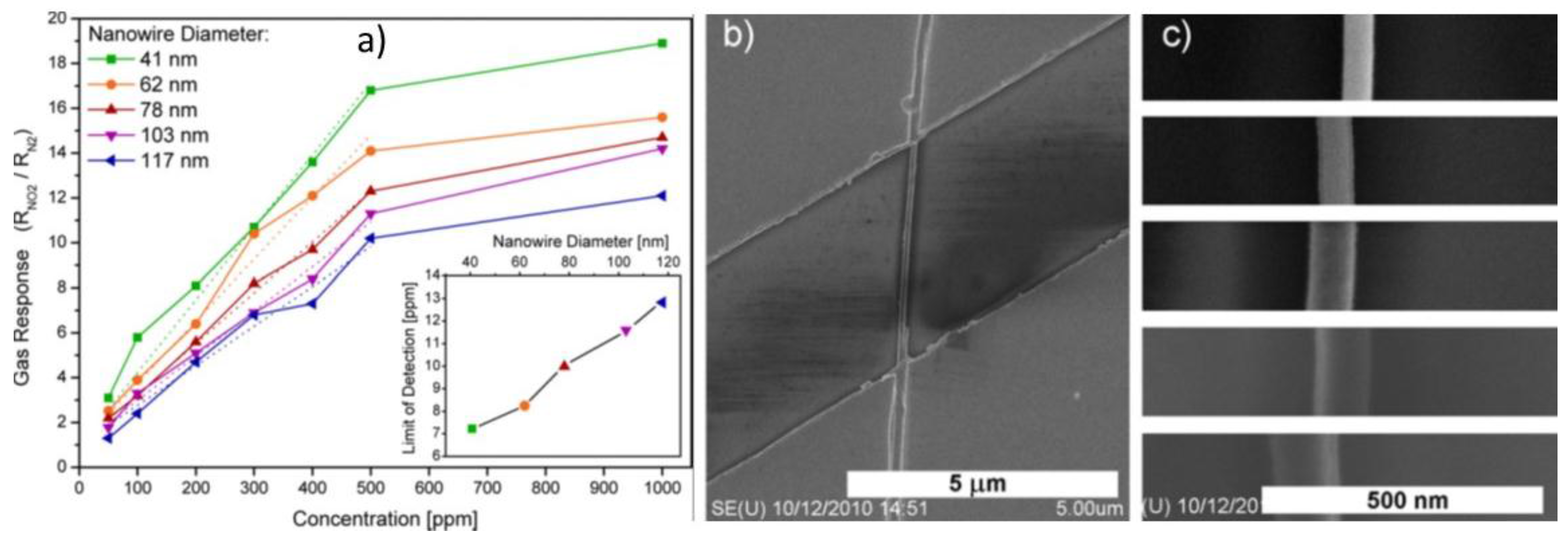
  57. Tonezzer, M.; Hieu, N.V. Size-dependent response of single-nanowire gas sensors. Sens. Actuators B: Chem. 2012, 163, 146–152. [Google Scholar] [CrossRef]
  58. Jung, T.-H.; Kwon, S.-I.; Park, J.-H.; Lim, D.-G.; Choi, Y.-J.; Park, J.-G. SnO2 nanowires bridged across trenched electrodes and their gas-sensing characteristics. Appl. Phys. A 2008, 91, 707–710. [Google Scholar] [CrossRef]
  59. Bolotov, V.V.; Roslikov, V.E.; Roslikova, E.A.; Ivlev, K.E.; Knyazev, E.V.; Davletkildeev, N. A Formation of two-layer composite-on-insulator structures based on porous silicon and SnO x. Study of their electrical and gas-sensing properties. Semiconductors 2014, 48, 397–401. [Google Scholar] [CrossRef]
  60. Jiménez, V.M.; Espinós, J.P.; González-Elipe, A.R. Effect of texture and annealing treatments in SnO2 and Pd/SnO2 gas sensor materials. Sens. Actuators B: Chem. 1999, 61, 23–32. [Google Scholar] [CrossRef]
  61. Du, X.; George, S.M. Thickness dependence of sensor response for CO gas sensing by tin oxide films grown using atomic layer deposition. Sens. Actuators B: Chem. 2008, 135, 152–160. [Google Scholar] [CrossRef]
  62. Ansari, S.G.; Gosavi, S.W.; Gangal, S.A.; Karekar, R.N.; Aiyer, R.C. Characterization of SnO2-based H2 gas sensors fabricated by different deposition techniques. J. Mater. Sci.: Mater. Electron. 1997, 8, 23–27. [Google Scholar]
  63. Brown, J.R.; Haycock, P.W.; Smith, L.M.; Jones, A.C.; Williams, E.W. Response behaviour of tin oxide thin film gas sensors grown by MOCVD. Sens. Actuators B: Chem. 2000, 63, 109–114. [Google Scholar] [CrossRef]
  64. Benkstein, K.; Martinez, C.; Li, G.; Meier, D.; Montgomery, C.; Semancik, S. Integration of nanostructured materials with MEMS microhotplate platforms to enhance chemical sensor performance. J. Nanopart Res. 2006, 8, 809–822. [Google Scholar] [CrossRef]
  65. Stoycheva, T.T.; Vallejos, S.; Pavelko, R.G.; Popov, V.S.; Sevastyanov, V.G.; Correig, X. Aerosol-Assisted CVD of SnO2 Thin Films for Gas-Sensor Applications. Chem. Vapor Depos. 2011, 17, 247–252. [Google Scholar] [CrossRef]
  66. Kwoka, M.; Ottaviano, L.; Szuber, J. Comparative analysis of physico-chemical and gas sensing characteristics of two different forms of SnO2 films. Appl. Surface Sci. 2015, 326, 27–31. [Google Scholar] [CrossRef]
  67. Larciprete, R.; Borsella, E.; De Padova, P.; Perfetti, P.; Faglia, G.; Sberveglieri, G. Organotin films deposited by laser-induced CVD as active layers in chemical gas sensors. Thin Solid Films 1998, 323, 291–295. [Google Scholar] [CrossRef]
  68. Liu, Y.; Koep, E.; Liu, M. A Highly Sensitive and Fast-Responding SnO2 Sensor Fabricated by Combustion Chemical Vapor Deposition. Chem. Mater. 2005, 17, 3997–4000. [Google Scholar] [CrossRef]
  69. Hui, H.; Lee, Y.C.; Tan, O.K.; Zhou, W.; Peng, N.; Zhang, Q. High sensitivity SnO 2 single-nanorod sensors for the detection of H 2 gas at low temperature. Nanotechnology 2009, 20, 115501. [Google Scholar]
  70. Moseley, P.T.; Williams, D.E. A selective ammonia sensor. Sens. Actuators B: Chem. 1990, 1, 113–115. [Google Scholar] [CrossRef]
  71. Dawson, D.H.; Henshaw, G.S.; Williams, D.E. Description and characterization of a hydrogen sulfide gas sensor based on Cr2-yTiyO3+x. Sens. Actuators B: Chem. 1995, 26, 76–80. [Google Scholar] [CrossRef]
  72. Pokhrel, S.; Li, X.; Huo, L.; Zhao, H.; Cheng, X. Investigation and characterization of radio frequency sputtered Cr1.8Ti0.2O3−δ thin films derived by citrate, sol–gel and solid state routes. Thin Solid Films 2007, 515, 7053–7058. [Google Scholar] [CrossRef]
  73. Pokhrel, S.; Huo, L.; Zhao, H.; Gao, S. Sol–gel derived polycrystalline Cr1.8Ti0.2O3 thick films for alcohols sensing application. Sens. Actuators B: Chem. 2007, 120, 560–567. [Google Scholar] [CrossRef]
  74. Nartowski, A.M.; Atkinson, A. Sol-Gel Synthesis of Sub-Micron Titanium-Doped Chromia Powders for Gas Sensing. J. Sol-Gel. Sci. Technol. 2003, 26, 793–797. [Google Scholar] [CrossRef]
  75. Neri, G.; Bonavita, A.; Rizzo, G.; Galvagno, S. Low temperature sol-gel synthesis and humidity sensing properties of Cr2−xTixO3. J. Eur. Ceramic Soc. 2004, 24, 1435–1438. [Google Scholar] [CrossRef]
  76. Chabanis, G.; Parkin, I.P.; Williams, D.E. Microspheres of the gas sensor material Cr2-xTixO3 prepared by the sol-emulsion-gel route. J. Mater. Chem. 2001, 11, 1651–1655. [Google Scholar] [CrossRef]
  77. Niemeyer, D.; Williams, D.E.; Smith, P.; Pratt, K.F.E.; Slater, B.; Catlow, C.R.A.; Stoneham, A.M. Experimental and computational study of the gas-sensor behaviour and surface chemistry of the solid-solution Cr2-xTixO3 (x ≤0.5). J. Mater. Chem. 2002, 12, 667–675. [Google Scholar] [CrossRef]
  78. Peter, C.; Kneer, J.; Schmitt, K.; Eberhardt, A.; Wöllenstein, J. Preparation, material analysis, and morphology of Cr2-xTi xO3+z for gas sensors. Phys. Status Solidi (A) Appl. Mater. Sci. 2013, 210, 403–407. [Google Scholar] [CrossRef]
  79. Jayaraman, V.; Gnanasekar, K.I.; Prabhu, E.; Gnanasekaran, T.; Periaswami, G. Preparation and characterisation of Cr2−xTixO3+δ and its sensor properties. Sens. Actuators B: Chem. 1999, 55, 175–179. [Google Scholar] [CrossRef]
  80. Li, C.C.; Yin, X.M.; Wang, T.H.; Zeng, H.C. Morphogenesis of Highly Uniform CoCO3 Submicrometer Crystals and Their Conversion to Mesoporous Co3O4 for Gas-Sensing Applications. Chem. Mater. 2009, 21, 4984–4992. [Google Scholar] [CrossRef]
  81. Pokhrel, S.; Ming, Y.; Huo, L.; Zhao, H.; Gao, S. Cr2-xTixO3 (x ≤ 0.5) as CH3COCH3 sensitive resistors. Sens. Actuators, B: Chem. 2007, 125, 550–555. [Google Scholar] [CrossRef]
  82. Conde-Gallardo, A.; Cruz-Orea, A.; Zelaya-Angel, O.; Bartolo-Pèrez, P. Electrical and optical properties of Cr2-xTixO 3 thin films. J. Phys. D: Appl. Phys. 2008, 41, 1–6. [Google Scholar] [CrossRef]
  83. Shaw, G.A.; Parkin, I.P.; Williams, D.E. Atmospheric pressure chemical vapour deposition of Cr2-xTixO3 (CTO) thin films ([less-than-or-equal]3 [small micro]m) on to gas sensing substrates. J. Mater. Chem. 2003, 13, 2957–2962. [Google Scholar] [CrossRef]
  84. Shaw, G.A.; Pratt, K.F.E.; Parkin, I.P.; Williams, D.E. Gas sensing properties of thin film (≤3 μm) Cr2−xTixO3 (CTO) prepared by atmospheric pressure chemical vapour deposition (APCVD), compared with that prepared by thick film screen-printing. Sens. Actuators B: Chem. 2005, 104, 151–162. [Google Scholar] [CrossRef]
  85. Du, J.; Wu, Y.; Choy, K.-L. Controlled synthesis of gas sensing Cr2−xTixO3 films by electrostatic spray assisted vapour deposition and their structural characterisation. Thin Solid Films 2006, 497, 42–47. [Google Scholar] [CrossRef]
  86. Du, J.; Wu, Y.; Choy, K.-L.; Shipway, P.H. Structure, properties and gas sensing behavior of Cr2 − xTixO3 films fabricated by electrostatic spray assisted vapour deposition. Thin Solid Films 2010, 519, 1293–1299. [Google Scholar] [CrossRef]
  87. Li, W.Y.; Xu, L.N.; Chen, J. Co3O4 Nanomaterials in Lithium-Ion Batteries and Gas Sensors. Adv. Funct. Mater. 2005, 15, 851–857. [Google Scholar] [CrossRef]
  88. Choi, K.-I.; Kim, H.-R.; Kim, K.-M.; Liu, D.; Cao, G.; Lee, J.-H. C2H5OH sensing characteristics of various Co3O4 nanostructures prepared by solvothermal reaction. Sens. Actuators B: Chem. 2010, 146, 183–189. [Google Scholar] [CrossRef]
  89. Jagadeesh, R.V.; Junge, H.; Pohl, M.-M.; Radnik, J.; Brückner, A.; Beller, M. Selective Oxidation of Alcohols to Esters Using Heterogeneous Co3O4–N@C Catalysts under Mild Conditions. J. Am. Chem. Soc. 2013, 135, 10776–10782. [Google Scholar] [CrossRef] [PubMed]
  90. Barreca, D.; Bekermann, D.; Comini, E.; Devi, A.; Fischer, R.A.; Gasparotto, A.; Gavagnin, M.; Maccato, C.; Sada, C.; Sberveglieri, G.; et al. Plasma enhanced-CVD of undoped and fluorine-doped Co3O4 nanosystems for novel gas sensors. Sens. Actuators B: Chem. 2011, 160, 79–86. [Google Scholar] [CrossRef]
  91. Ghosh, P.K.; Das, S.; Kundoo, S.; Chattopadhyay, K.K. Effect of Fluorine Doping on Semiconductor to Metal-Like Transition and Optical Properties of Cadmium Oxide Thin Films Deposited by Sol–Gel Process. J. Sol-Gel. Sci. Technol. 2005, 34, 173–179. [Google Scholar] [CrossRef]
  92. Jinling, Y.; Jingkui, L.; Duo, J.; Shi, Y.; Weihua, T.; Guanghui, R. The influence of fluorine on the structures and properties of Pr2-xSrxCuO4-y (X = 0.0, 0.4, 1.0). J. Phys.: Condens. Matter 1997, 9, 1249. [Google Scholar]
  93. Liu, B.; Gu, M.; Liu, X.; Huang, S.; Ni, C. First-principles study of fluorine-doped zinc oxide. Appl. Phys. Lett. 2010, 97, 122101. [Google Scholar] [CrossRef]
  94. Singh, N.; Yan, C.; Lee, P.S. Room temperature CO gas sensing using Zn-doped In2O3 single nanowire field effect transistors. Sens. Actuators B: Chem. 2010, 150, 19–24. [Google Scholar] [CrossRef]
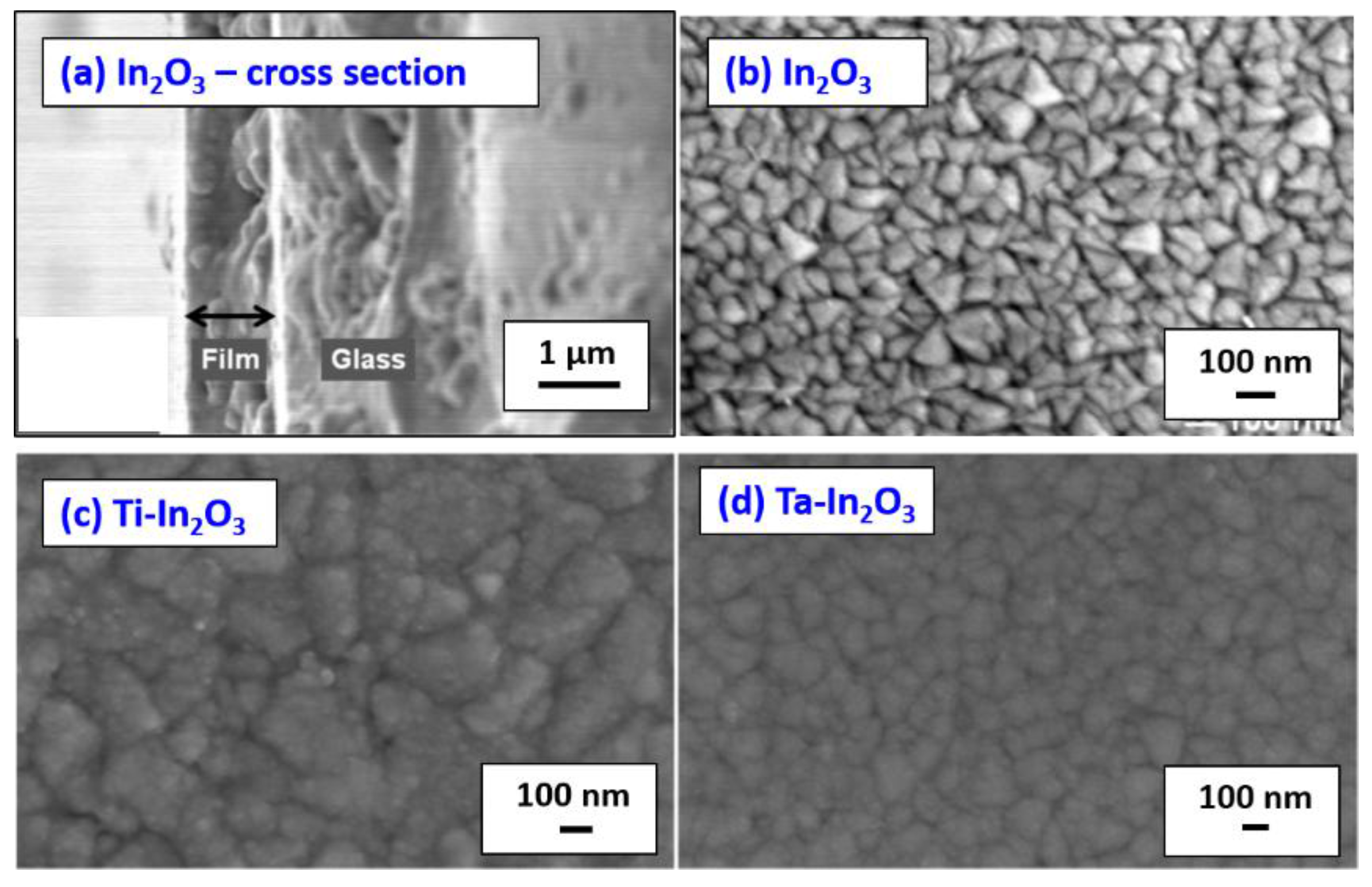
  95. Bloor, L.G.; Manzi, J.; Binions, R.; Parkin, I.P.; Pugh, D.; Afonja, A.; Blackman, C.S.; Sathasivam, S.; Carmalt, C.J. Tantalum and Titanium doped In2O3 Thin Films by Aerosol-Assisted Chemical Vapor Deposition and their Gas Sensing Properties. Chem. Mater. 2012, 24, 2864–2871. [Google Scholar] [CrossRef]
  96. Salehi, A.; Gholizade, M. Gas-sensing properties of indium-doped SnO2 thin films with variations in indium concentration. Sens. Actuators B: Chem. 2003, 89, 173–179. [Google Scholar] [CrossRef]
  97. Salehi, A. Selectivity enhancement of indium-doped SnO2 gas sensors. Thin Solid Films 2002, 416, 260–263. [Google Scholar] [CrossRef]
Figure 1. Scanning electron microscope images of WO3 nanostructures grown at (a) low and (b,c) high magnification grown localized on microhotplates via AACVD. Adapted from [23].
Chemosensors 04 00004 g001
Figure 2. Relative sensor response (R) to ppm concentration (C) of NO2, C2H5OH and CO against operating temperature for different tungsten oxide morphologies (based on the maximum response for the minimum concentration in Table 1 for each morphology/gas combination).
Chemosensors 04 00004 g002
Figure 3. Scanning electron microscope images of (a) nanowire mat (b) NP films. Adapted from [32].
Chemosensors 04 00004 g003
Figure 4. Relative sensor response (R) to ppm concentration (C) of H2, C2H5OH and CO against operating temperature for different zinc oxide morphologies (based on the maximum response for the minimum concentration shown in Table 2 for each morphology/gas combination). Other structures: NR, NB, CL, flakes.
Chemosensors 04 00004 g004
Figure 5. SEM images of a ZnO wire with curved (a) and straight (b) sides. Reprinted from [36] with permission from Springer.
Chemosensors 04 00004 g005
Figure 6. Relative sensor response (R) to ppm concentration (C) of H2, C2H5OH and NO2 against operating temperature for different tin oxide morphologies (based on the maximum response for the minimum concentration shown in Table for each morphology/gas combination). Other structures: NR and plates.
Chemosensors 04 00004 g006
Figure 7. Gas responses of five single nanowire (SNW) sensors to various NO2 concentrations at 250 °C (a), and SEM images of a single nanowire connected to the electrodes (b) and and the NWs with different diameters (c) (from the bottom to the top: 117, 103, 78, 62, and 41 nm). Reprinted from [57] with permission from Elsevier.
Chemosensors 04 00004 g007
Figure 8. SEM photographs of Cr1.8Ti0.2O3 films deposited at 650 -C from the different precursor without additive (a) 0.05 M, (b) 0.005 M, and with additive (c) 0.05 M, (d) 0.005 M. Reprinted from [85] with permission from Elsevier.
Chemosensors 04 00004 g008
Figure 9. SEM images of Zn-In2O3 NWs at (a) low and (b) high magnification. Reprinted from [94] with permission from Elsevier.
Chemosensors 04 00004 g009
Figure 10. SEM images of (a) In2O3 cross section, (b) In2O3, (c) Ti- In2O3 and (d) Ta-In2O3. Reprinted from [95] with permission from American Chemical Society.
Chemosensors 04 00004 g010
Figure 11. Maximum gas response of doped and undoped In2O3 against different gases at optimum operating temperature. Reprinted from [95] with permission from American Chemical Society.
Chemosensors 04 00004 g011
Table 1. Summary of the features and sensing properties reported for chemical vapour deposited tungsten oxide.
Prec.CVD methodTdep °CFormFeatures nmSensor
type
Top °CppmGasRtres
s
Ref.
W(OCl4)PE-film-Ω20010NO248-[21]
WCl6AP625film3600TΩ40020C2H5OH8.5-[20]
W(CO)6LP500NPs140ØΩ>4505000H2***-[22]
WHF-NPs100ØΩ501NO24701-[16]
WO3EB-NPs9Ø
200T
NS*10010NH3--[18]
WCMPLXAA500P1000Ø
30,000T
Ω55020C2H5OH5.1-[27]
WHF800NWs-Ω4501N2O4.41175[17]
W(OPh)6AAEF-NWsΩ2500.8NO2120-[26]
W(CO)6AAL°c580NWs100–400ØΩ37580CO8-[23]
W(OPh)6AA400NWs60–120Ø
7000L
Ω150100CO
 
5-[25]
W(OPh)6AA400NWs60–120Ø
7000L
Ω2001C6H621114[29]
W(CO)6AA500NWs50–100Ø
11000L
Ω3900.4NO2250-[24]
W(CO)6AA390NWs50–100Ø
10,000L
Ω190
220
100
100
C7H8
C2H5OH
3
3.5
450
-
[30]
WO2.9CVD400NRs30–110Ø
1000T
ORT65**H2O2.16
 
-[19]
Prec: precursors, Tdep: temperature of deposition, Top: operating temperature, tres: response time, ppm: parts per millon, R = Ra/Rg (oxidative gas), R = Rg/Ra (reductive gas), CMPLX: [nBu4N]2[W10O32], PE: plasma enhanced, AP: atmospheric pressure, LP: low pressure, HF: Hot Filament, EB: Electron Beam, AA: Aerosol assisted, EF: Electric field, L°c: Localized, O: optical, Ω: resistive, NS: noise spectroscopy, *: gas sensing assisted by Blue-LED, **: % Relative humidity, ***: low response and not stable, NPs: nanoparticles, NWs: nanowires, NRs: nanorods, Ø: diameter, T: film thickness, L: length.
Table 2. Summary of the features and sensing properties reported for chemical vapour deposited zinc oxide.
Prec.CVD
method
Tdep
°C
FormFeatures
nm
Sensor
Type
Top
°C
ppmgasRtres
s
Ref.
Et2ZnMO-Film130FTΩ3001660CO1.6-[44]
Et2ZnPE-Film
 
500 FT
38 CZ
Ω +ORT200000O21.8-[45]
ZnCMPLXAA450Film25CZΩ60500C2H5OH210[51]
Et2ZnMO450NPs-Ω3001000CO1.53-[46]
Zn(OAc)2AA350NPs12CZΩ30010000DMA1.7240[52]
ZnCVD550NWs30000ØΩ+OSNWRT200C2H5OH2-[36]
ZnOCVD-NWs130Ø
4000L
Ω+OSNW2001×106CO4-[53]
ZnCVD-NWs80Ø
3500L
FETSNW-400CO3-[37]
ZnUHV650NWs100ØΩ+OSNWRT100H21.353[38]
Et2ZnMO500NRs100ØΩ300500O23.5-[47]
ZnCVD600NRs-Ω+ORT2.5O3130045[39]
ZnPE-NRs100Ø
2000L
Ω400 CH2O100-[40]
ZnCVD700HS-ΩRT250CO1.8-[41]
ZnVT700HS800TB
150TC
FETSNW2001NO22-[42]
ZnCMPLXPE300HS Ω1000.28O31000-[49]
ZnVT410HS5000ØΩ400205CH2O38-[43]
ZnCMPLXPE300HS Ω4005000H214-[50]
Zn(NO3)2C1100F20000Ω SF400500C2H5OH15.3-[48]
Prec: precursors, Tdep: temperature of deposition, Top: operating temperature, tres: response time, ppm: parts per millon, R = Ra/Rg (oxidative gas), R = Rg/Ra (reductive gas), Et2Zn: Diethylzincm, CMPLX: complex Ω: resistive, O: optical, SNW: single nanowire configuration, SF: single flake, FT: film thickness, Ø: diameter, L: length, CZ: Crystallite size, TC: thickness of the combs, TB: thickness of the NBs, NWs: nanowires, NPs: nanoparticles, NRs: nanorods, HS: hierarchical structures, F: flake, DMA: Dimethylamine.
Table 3. Summary of the features and sensing properties reported for chemical vapour deposited tin oxide.
Prec.CVD
method
Tdep,
°C
FormFeatures,
nm
Sensor
type
Top
°C
ppmgasRtres
s
Ref.
SnCl2.2H2OCVD-Film100TΩ-6NO21.2-[59]
TTBMO350Film50TΩRT5H2S1.1-[63]
SnCl4IBIRTFilm400TΩ500-H2--[60]
SnCl4ALD250Film2.6TΩ300-CO43-[61]
TMHLE-NPs~15ØΩ20020NO277160[66,67]
Sn(NO3)4Loc375NPs-Ω-200CH4O5-[64]
T-crownAA400NPs18–36ØΩ30010NO21.7-[65]
TEHC850NPs1000ØΩ300500C2H5OH107531[68]
SnCl2.2H2OCVD375P-Ω240300H21.03-[62]
SnCVD750NWs-Ω 400CO3.910[56]
SnCVD800NWs41ØΩSNW300500NO2173[57]
DBTAPE-NRs1200L
45Øb-10Ø
ΩSNW250100H213-[69]
SnCVD800NWs
 
60Ø
20,000L
Ω2001NO2908[58]
TTBCVD700Plates30–40TΩ250100C2H5OH1.510[55]
Prec: precursors, Tdep: temperature of deposition, Top: operating temperature, tres: response time, ppm: parts per millon, R=Ra/Rg (oxidative gas), R=Rg/Ra (reductive gas), TTB: Tin(IV)tert-butoxide, TEH: Tin(II)ethylhexanoate, T-crown: Sn(18-crown-6)Cl4, TMH: Tetramethyltin, DBTA: dibutyltin diacetate, LE: laser enhanced, Loc: Localized, PE: plasma enhanced, C: combustion, IBI: ion beam induced, P: particles, NPs: nanoparticles, Ø: diameter, Øb: diameter at the base of nanostructure, T: film thickness, L: length, NWs: nanowires, NRs: nanorods. Ω: resistive, SNW: single nanowire configuration.
Table 4. Summary of the features and sensing properties reported for chemical vapour deposited complex metal oxides.
MaterialPrec.CVD
Method
Tdep
°C
FT
nm
Top
°C
ppmgasRRef.
Co3O4:FCo(dpm)2
Co(hfa)2·TMEDA
PE200
300
400
200100Acetone [90]
Cr2O3:TiCr(acac)3
Ti-butoxide
AA550150-1000 [82]
Cr2O3:TiCrO2Cl2
TiCl4
AP400
475
550
500
1000
1500
40080CH3CH2OH
 
3.1
1.7
1.1
[83,84]
Cr2O3:TiChromium acetate
Ti(acac)2OiPr2
ESAVD650 200
300400500
500NH31.05
1.18
1.22
1.46
[85,86]
In2O3:TaInMe3
Ta(NMe2)5
AA550650500100
0.08
CH3CH2OH
NO2
16.9
3.01
[95]
In2O3:TiInMe3
Ti(NMe2)4
AA550790500100
0.08
CH3CH2OH
NO2
2.62
1.80
[95]
In2O3:ZnZnO
In2O3
CVD400-550 RT1-5CO [94]
SnO2:InSnCl4
InCl3
CVD40020050-2501000H2
Methanol
CO
1.14
1.23
1.20
[96,97]
Prec: precursors, Tdep: temperature of deposition, Top: operating temperature, ppm: parts per millon, R=Ra/Rg (oxidative gas), R=Rg/Ra (reductive gas), FT: film thickness, ES: Electrostatic spray assisted vapour deposition, PE: plasma enhanced, TMA: Trimethylamine, acac: cetylacetone, Me: methyl, TMEDA: tetramethylethylenediamine.

