1. Introduction
Current and future mobile communications need to deal with high data and video traffic which needs to be transmitted within a limited bandwidth, mainly because the user is now more attracted by the social media contents, online gaming, and video streaming, as well as the Internet of Things (IoTs) technology revolution. So, the LTE-Advanced generation (5G) targets can be achieved by using several technologies. Some of these technologies are beam forming, carrier aggregation, massive MIMO, and more complex modulation schemes, where the modulated signal will have a high signal envelope that increases the peak to average power ratio (PAPR). With simple amplifiers, there is inevitably a trade-off between high efficiency and linearity. So, to keep the linearity requirements of any communications standard, the amplifier device has to be backed off from the saturation point (most efficient point) due to high PAPR, into a region where most of the average input signal occurs, because at this region, the efficiency of the amplifier drops sharply. Working in the back-off region of the power amplifier means a significant amount of the DC power will be lost as heat, which means that less efficiency will be achieved [
1]. Modern power amplifiers should be designed to deal with high input PAPR, so that, it should work with a large output power back-off (OBO) with high efficiency. Known techniques for efficiency enhancements include the Doherty power amplifier (DPA), Envelope Elimination and Restoration (EER), Envelope Tracking (ET), Chireix Out-phasing and Linear amplification using Nonlinear Components (LINC). However, the most straightforward technique of obtaining good efficiency and linearity concurrently is the Doherty amplifier, where neither signal processing blocks nor additional controlling circuits are needed [
2,
3,
4,
5,
6,
7,
8].
In this paper,
Section 2 presents the Doherty concepts, after which design steps will be discussed in
Section 3.
Section 4 will show the results obtained for an example of an asymmetrical Doherty power amplifier applicable to a 5G base station, and finally, conclusions will be given.
2. Doherty Concept
In 1936, W. H. Doherty introduced a new combiner [
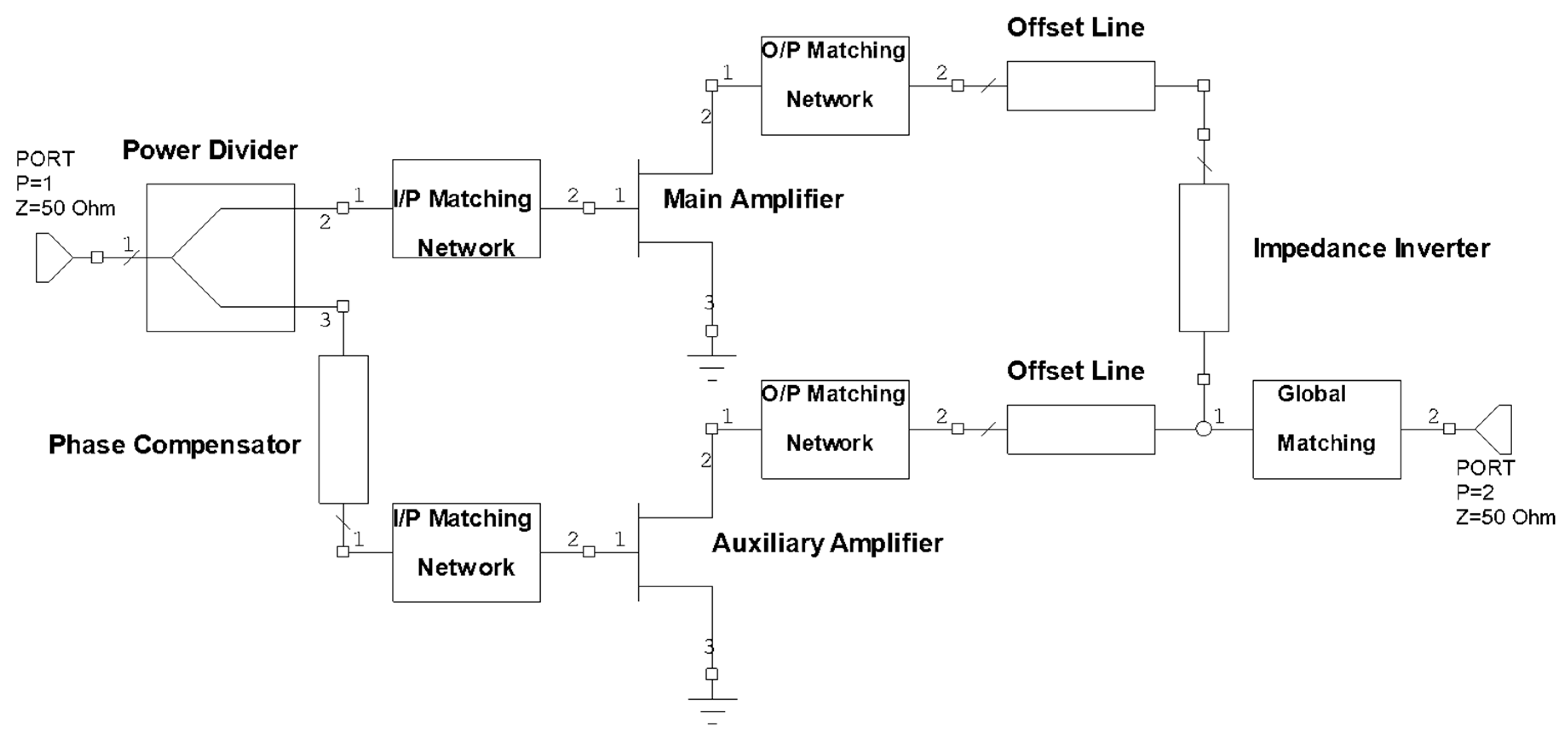
4] which was used in a broadcasting station based on high power tube amplifiers. The output of two amplifiers can be combined to achieve a nearly linear final output power by using λ/4 transmission lines. Two amplifiers, which are the carrier (main) amplifier and the auxiliary (peaking) amplifier, are used in the classical Doherty power amplifier as illustrated in
Figure 1. The main difference between the two amplifiers is their bias condition, where a class AB amplifier is used for the carrier amplifier and a class C amplifier is used for the auxiliary amplifier biasing. At the input side, a power divider is applied to the split input signal between the two amplifiers, where at the back-off input power level, the carrier amplifier should be saturated. Above this level, the auxiliary amplifier injects a current to the load until maximum designed output powers of both amplifiers are reached where the saturation occurs.
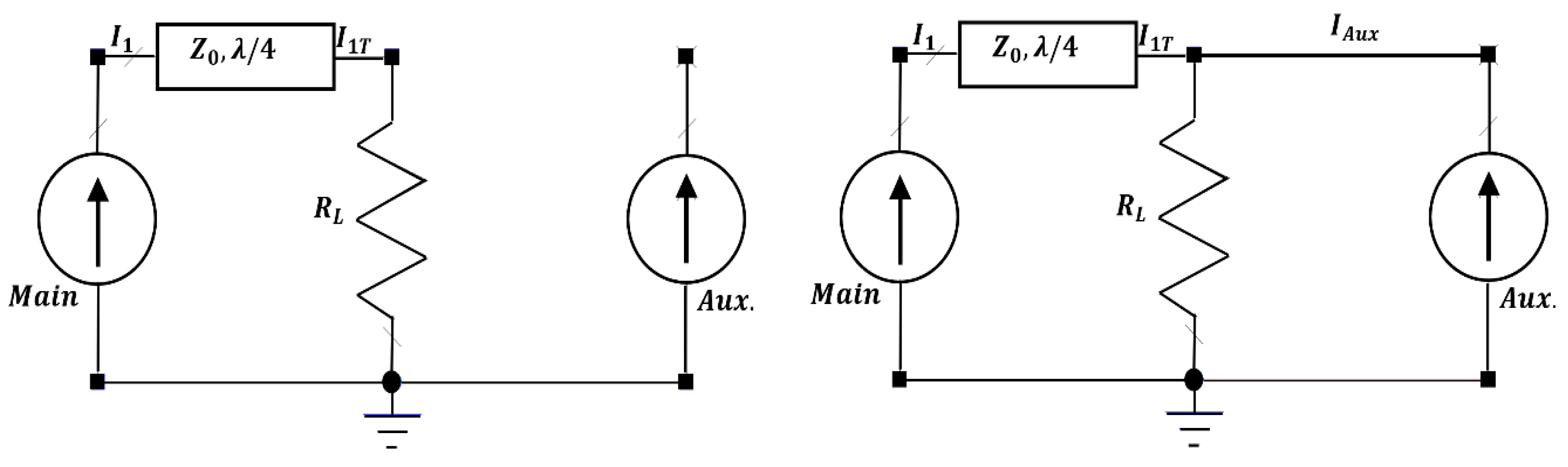
The active load-pull technique is used in the Doherty amplifier [
1]. Three regions of operation can be observed which are: The low input power region, where the auxiliary amplifier is off due to its biasing condition and the input power level is not enough to turn it on, whereas the carrier amplifier is working. In this case, the auxiliary amplifier can be represented as high impedance (ideally open circuit). Hence, a high load impedance will be seen by the carrier amplifier as a result of the λ/4 transmission line effect (Impedance Inverter). In this case, the carrier amplifier will be saturated as illustrated in
Figure 2a. The impedance seen by the carrier amplifier is given by:
where:
The medium input power region, where the auxiliary amplifier turns on and starts acting as an additional current source by contributing more current into the load and where the overall output power will be increased, is shown in
Figure 2b. The apparent load impedance seen by the inverter, at the summing node, will be increased as the auxiliary amplifier current increases. Hence, the carrier amplifier will see less impedance, but it remains almost saturated. In this case, the total output power will be increased as the total current is increasing, as illustrated by these equations:
where:
.
.
.
The third region (the high input power region), where the carrier and auxiliary amplifiers give their maximum output current, and the impedance is seen by both carrier and auxiliary amplifiers, depends on Equations (2) and (3).
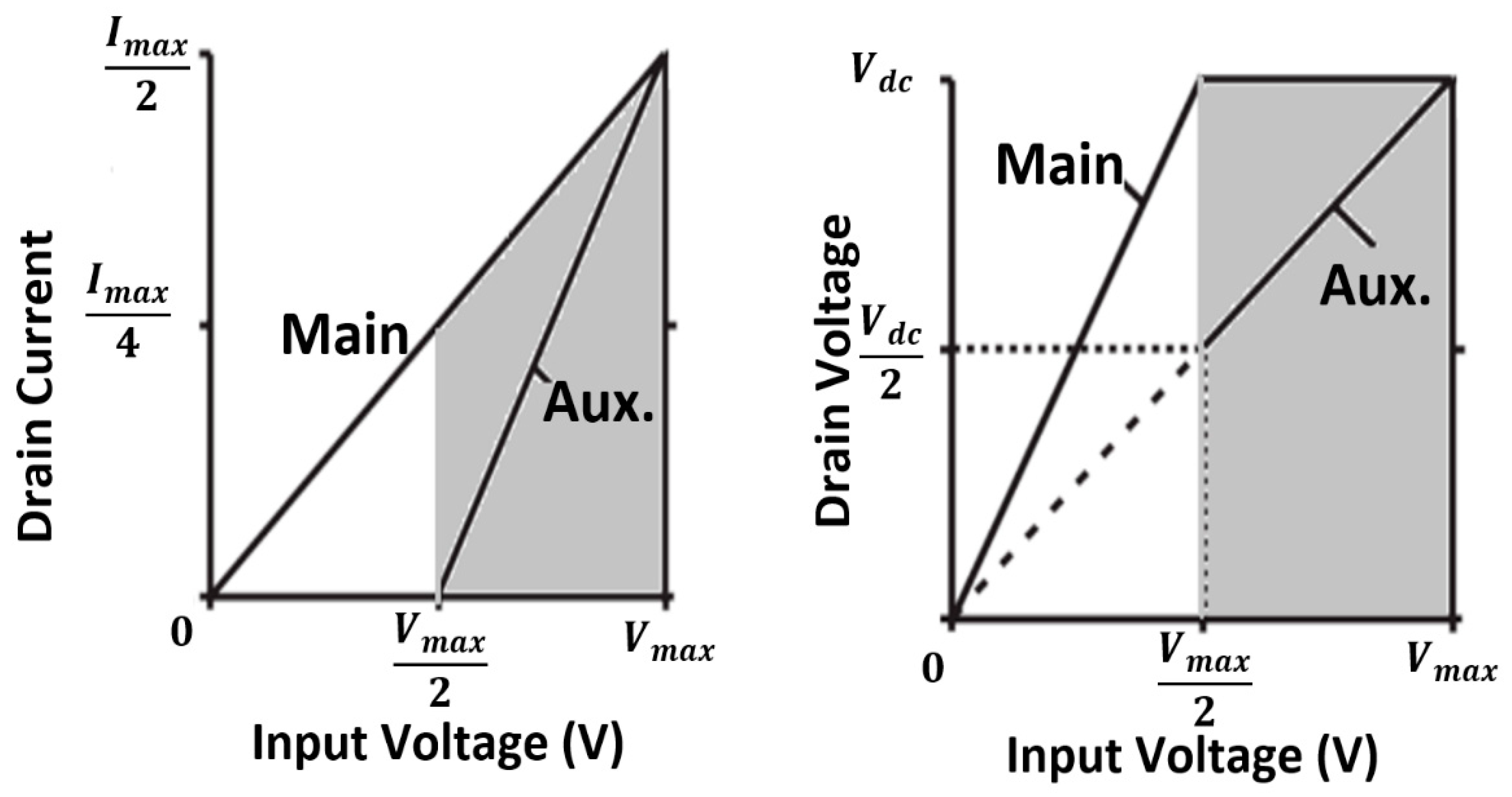
Figure 3 shows the behaviour of the voltage and current of the Doherty amplifier [
1]. It can be observed that after the OBO point, the carrier amplifier output voltage remains constant but its current increases, whereas the auxiliary amplifier is off until near the OBO point where after that, it starts injecting the current.
3. Doherty Amplifier Design
Generally, a power amplifier circuit can be divided into three sub-circuits, which are the stability circuit, input matching, and output matching network. Stability is an important parameter, that should be considered firstly, in designing any power amplifier so that no oscillation can occur. The input matching network is used for controlling the gain flatness over the intended frequency range; whereas the output matching network can be optimized to a trade-off between the maximum output power and the utmost efficiency, where load-pull technique should be applied to determine the optimum impedance. As mentioned above, the biasing conditions of both amplifiers are the main difference in their design.
In terms of the Doherty design, the output back-off of the complete amplifier is controlled by the compressed power ratio (δ) of the auxiliary amplifier to the carrier amplifier. This ratio can affect:
The sum of the peak output powers of both amplifiers gives the maximum achievable power (peak power), whereas the output back-off (average power) can be calculated using the following equation:
where
δ is the power ratio between the maximum achieved power of the auxiliary amplifier to the maximum achieved power of the carrier amplifier.
In the design presented, GaN High Electron Mobility Transistors (HEMTs) were used for both carrier and auxiliary amplifiers, because GaN HEMT devices have smaller capacitance at both the input and output sides, due to their high transition frequency and small periphery. Current GaN HEMTs have high efficiency, good broadband performance, and high breakdown voltage, due to their properties such as wide bandgap, high carrier concentration, and electron saturation velocities. This technology is used in most modern PA designs for higher frequencies because it has given the designers a better ability to design an efficient broadband PA. A minor drawback is that biasing for this technology is more complex, where different voltage polarity should be applied at the gate and drain sides, with the negative gate bias being applied first to prevent high current flow. Here, two GaN power transistors are used for the carrier and the auxiliary amplifiers, their capabilities being 25 W and 45 W, respectively. For this case, the maximum achievable power will be 48 dBm, and according to Equation (4), the maximum back-off that can be achieved is 8.9 dB. In this study, 8 dB power back-off was the target.
The biasing of the auxiliary amplifier should be as class C, where the amount of class C deepness can be controlled by the gate voltage. Hence, this controls the starting point for an auxiliary amplifier for current injection, where the load-modulation occurs, where the input level will be reduced by the amount of class C gate voltage deepness.
In addition, the line offset might be used (depending on the auxiliary output matching impedance characteristics) in the Doherty amplifier between the summing node and the auxiliary amplifier, in order to produce a high impedance toward the auxiliary amplifier when it is off. For this design case, a line offset of 50 Ω characteristic impedance with an electrical length of 40.6° is needed. Moreover, at the input of the auxiliary amplifier, an additional line offset is required to maintain the phase offset between the two amplifiers, due to the difference in the biasing condition.
4. Results
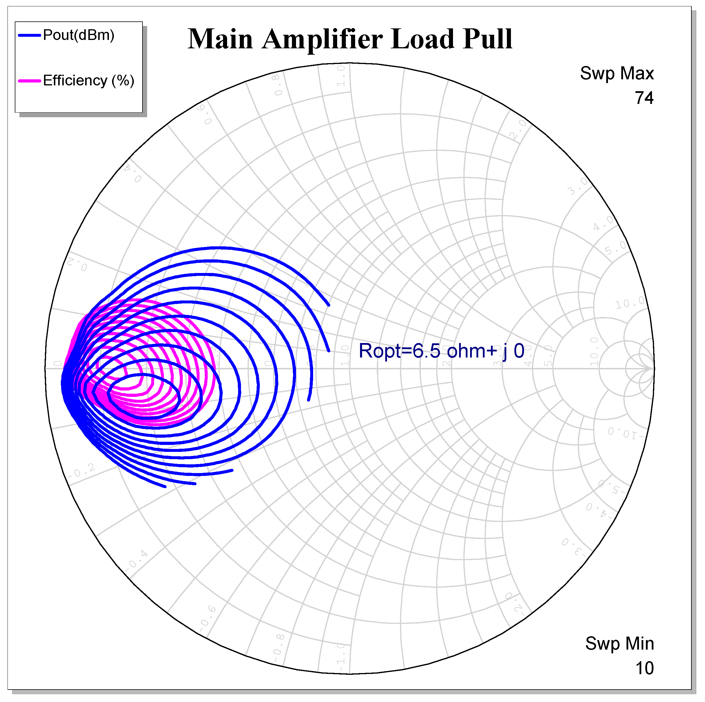
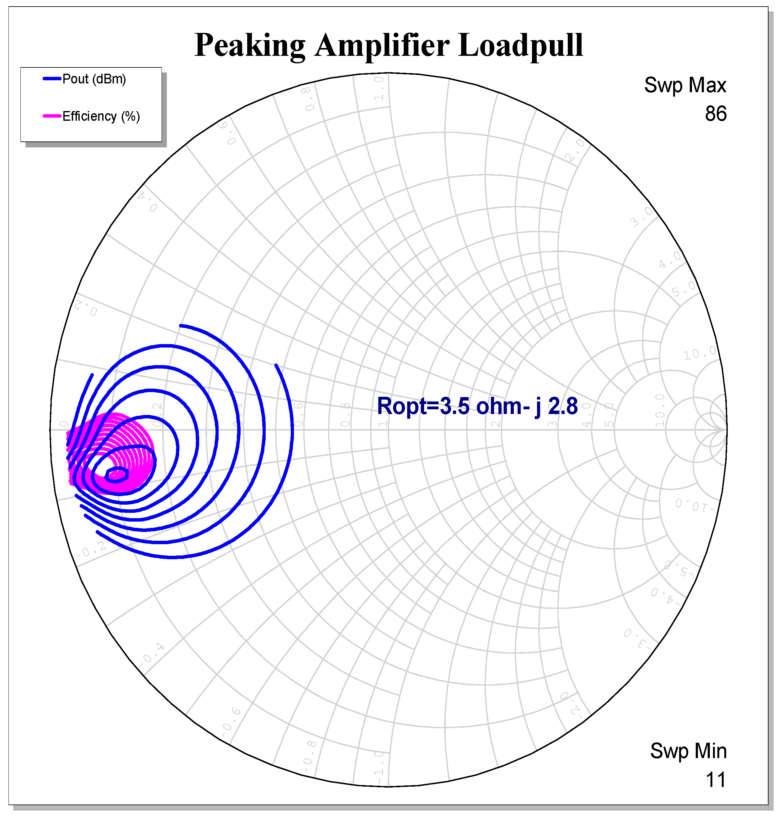
AWR MWO software (AWR Corporation, El Segundo, CA, USA) was used to perform the simulation, where the substrate material used in the design was Rogers RO4350B (Global Headquarters, Chandler, AZ, USA). After stabilizing both amplifiers, the load-pull analysis was performed in order to determine the optimum load impedance that the transistor needs to see, as shown in
Figure 4 and
Figure 5. It can be seen that the main amplifier needs to see a pure resistance of 6.5 Ω to give about 80%, whereas the peaking amplifier needs to see a complex load impedance of 3.5–2.8 Ω.
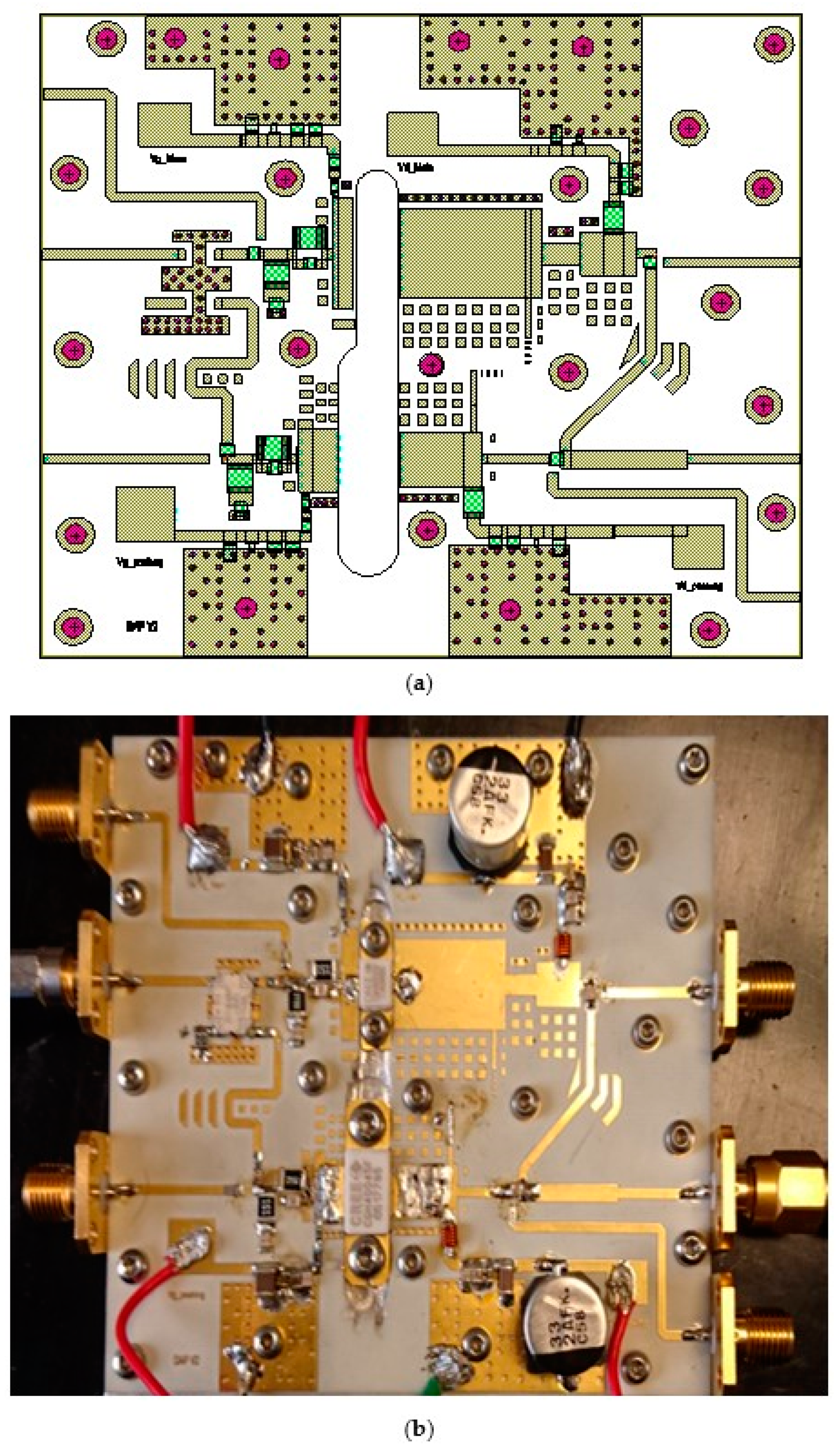
After that, both amplifiers’ circuits were designed and fabricated as shown in
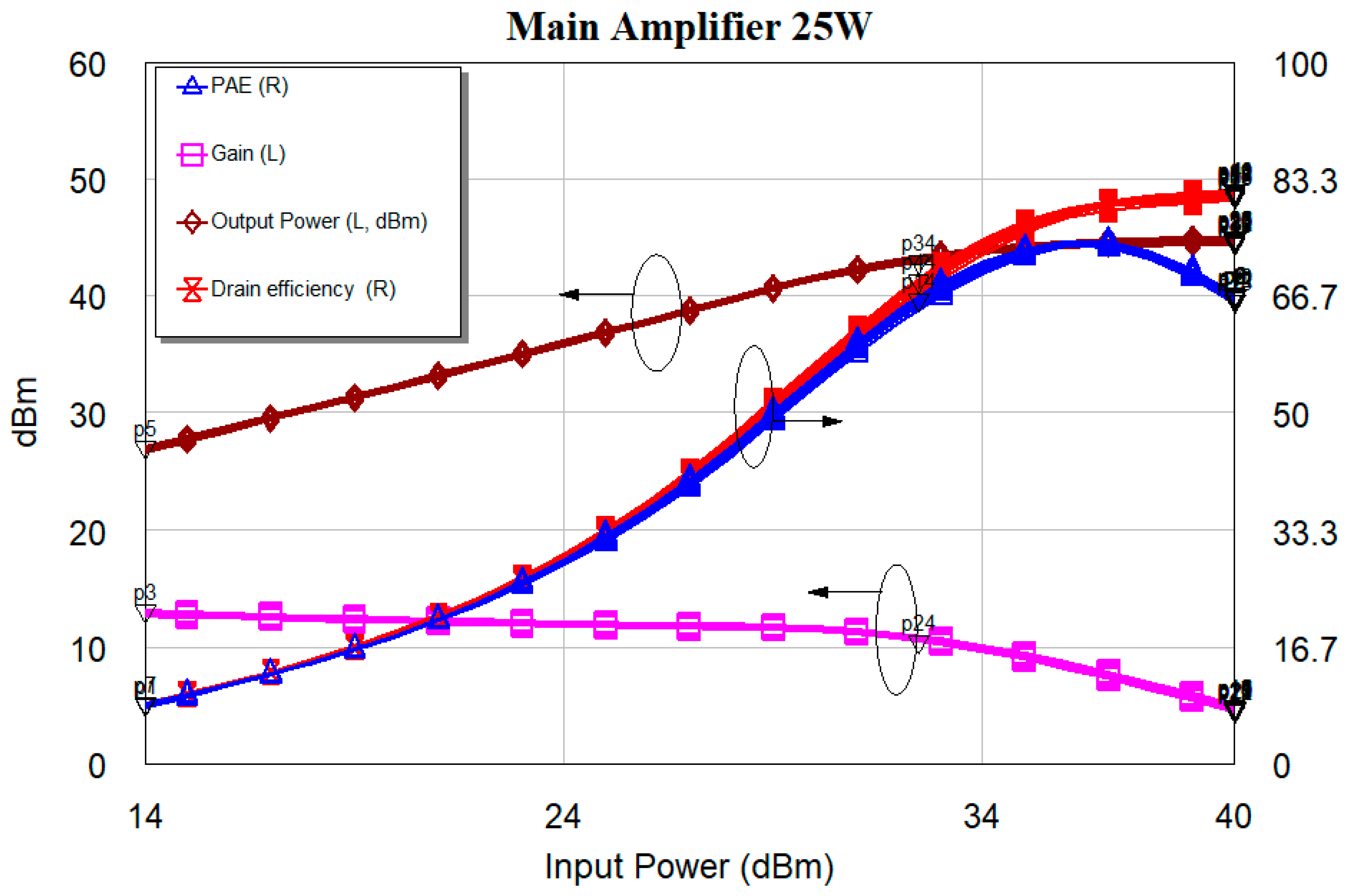
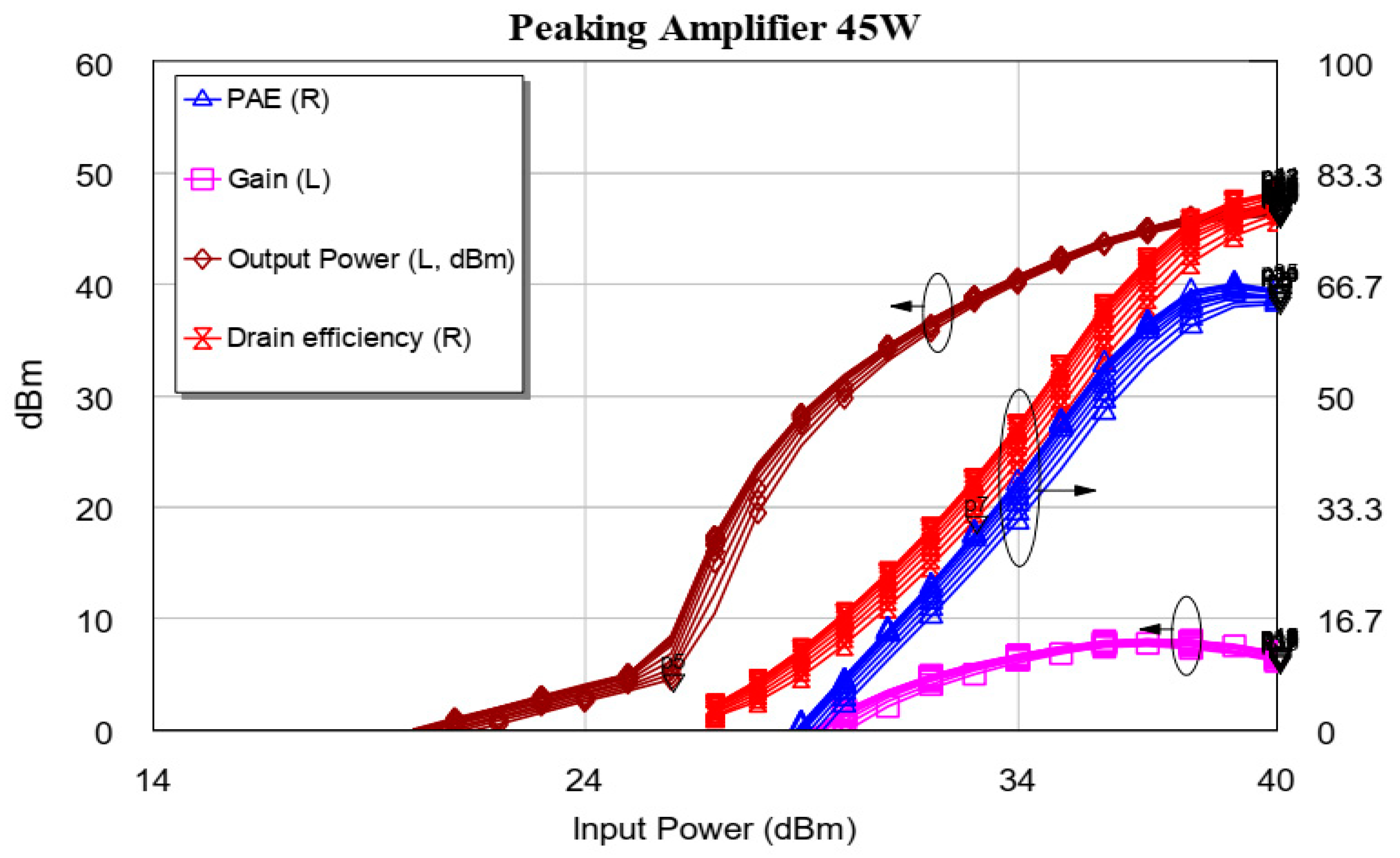
Figure 6. The amplifiers are designed to work in 3.3–3.5 GHz, where the performance of each designed amplifier, in terms of gain, output power, power added efficiency (PAE) and drain efficiency, and are shown in
Figure 7 for the carrier amplifier and
Figure 8 for the auxiliary amplifier. It is cleared at the back-off, and afterward, the auxiliary amplifier starts injecting the current due to biasing condition.
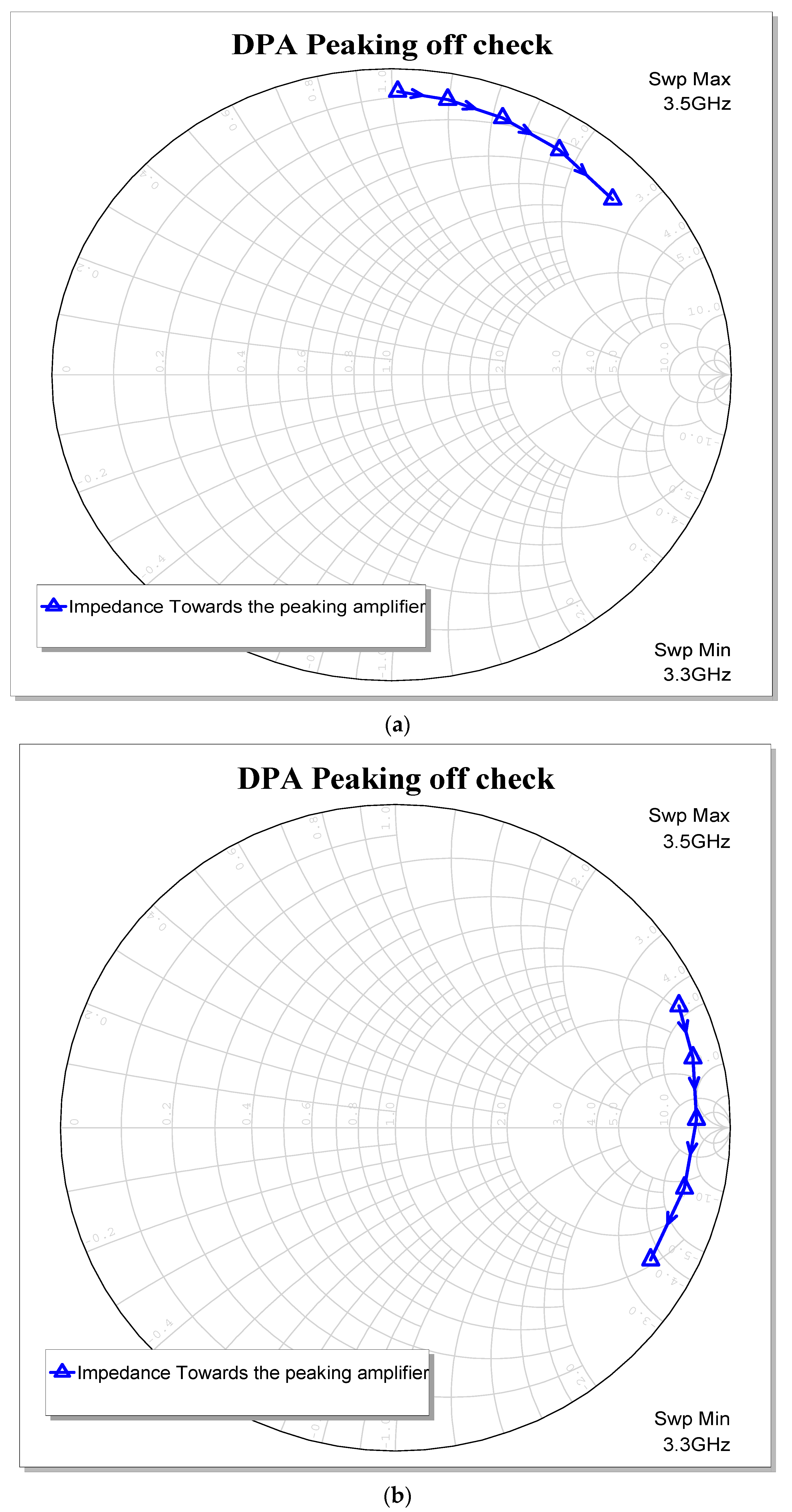
As mentioned previously, there is a need to add a line offset to the output of the auxiliary amplifier.
Figure 9a shows the impedance seen from the summing point toward the auxiliary amplifier when the transistor is off. It can be noticed that after adding the line offset, high impedance has been achieved, as shown in
Figure 9b.
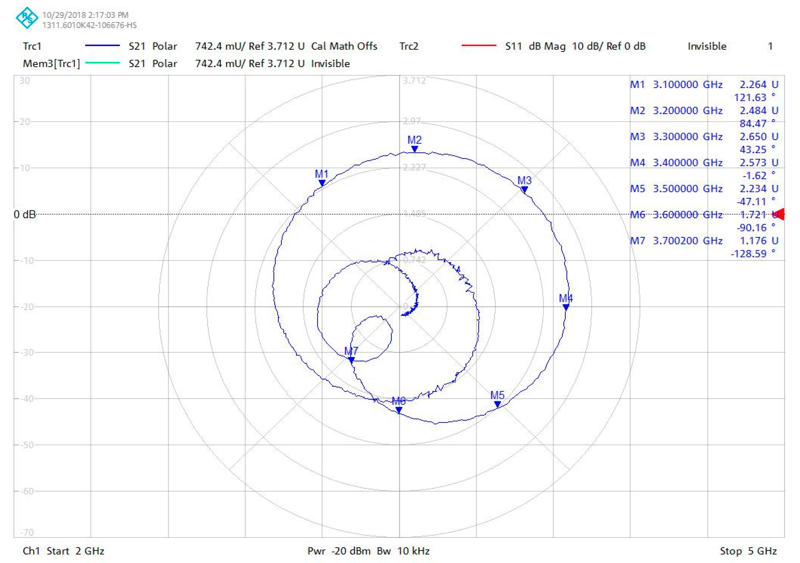
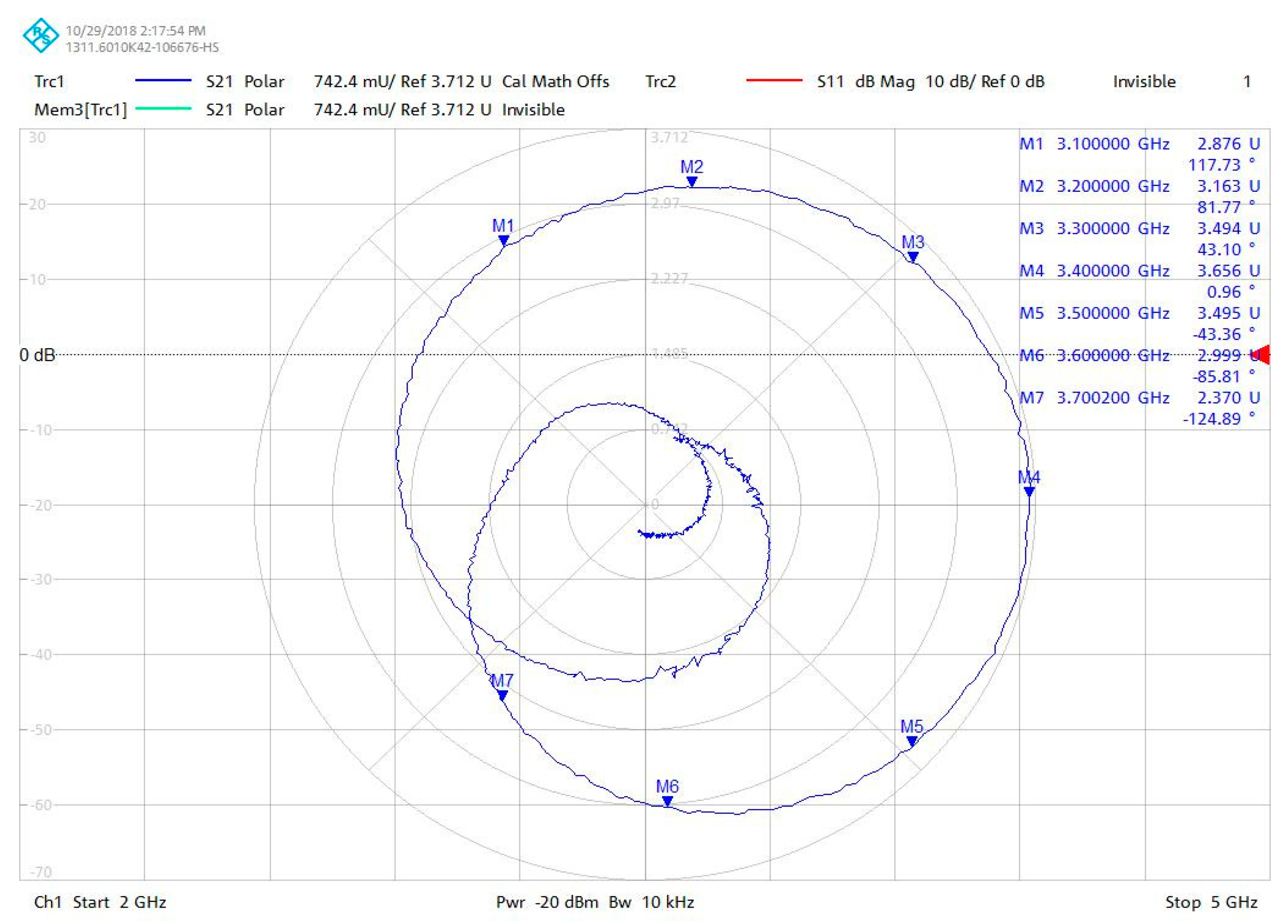
In terms of the small signal measurements, the gain phase measurement was used as a tool for illustrating and tuning the phase difference between the output of the two amplifiers. In the Doherty amplifier, there are two cases: The first is when only the main amplifier is working, and the other is when both amplifiers are working. The output signals of the amplifiers should be in-phase, so that both amplifiers’ currents can be combined to perform the load-modulation at the summing point.
Figure 10 and
Figure 11 show the Doherty amplifier gain phase (S
21) when only the carrier amplifier is working and when both amplifiers are ON. Respectively, it can be noticed that there is a minimal variation in the phase when both amplifiers are ON. This means that the output signals of both amplifiers are in phase. These measurements have been achieved by changing the biasing condition of the peaking amplifier so that the status of the peaking amplifier can be changed from OFF to ON.
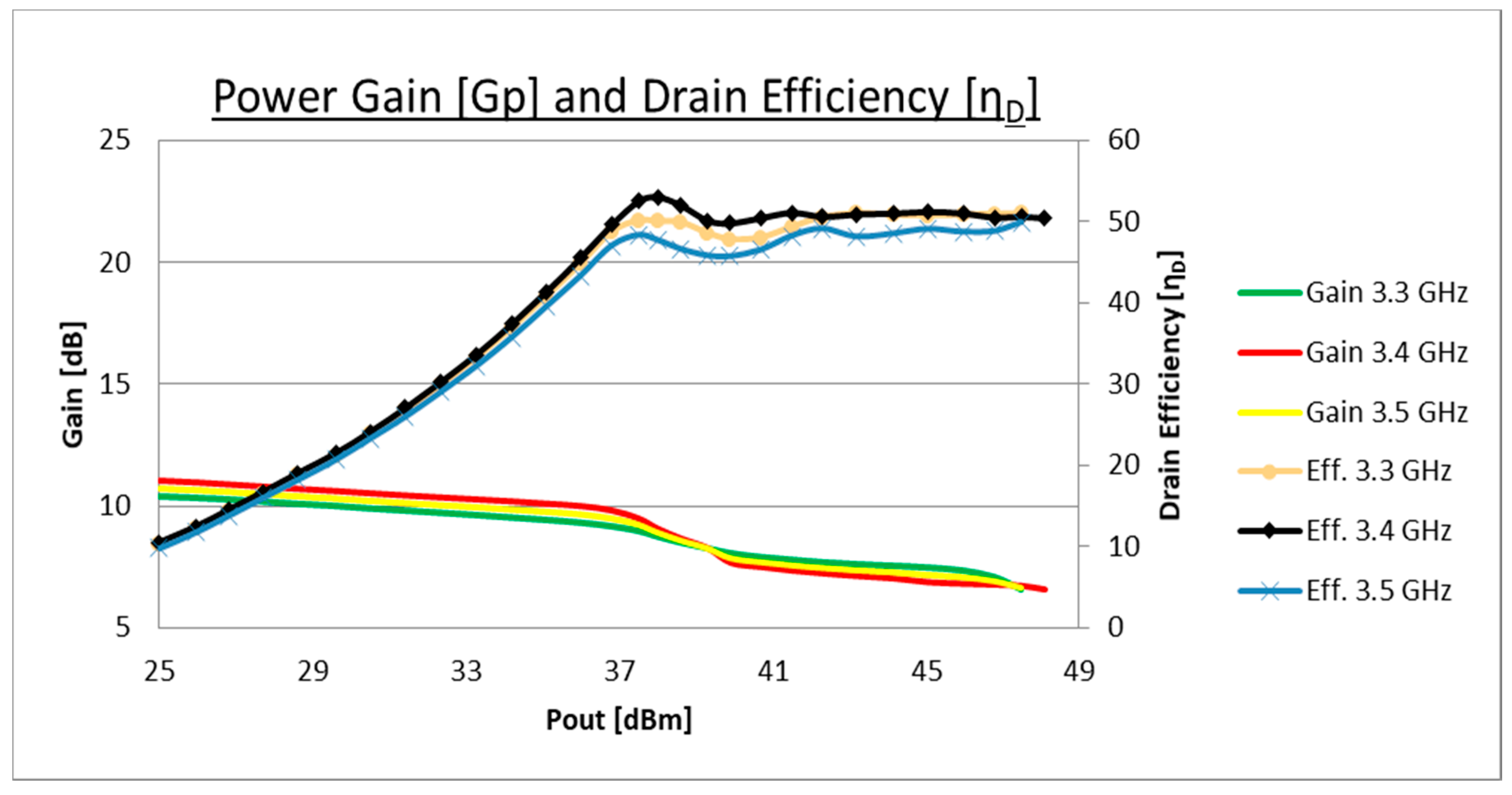
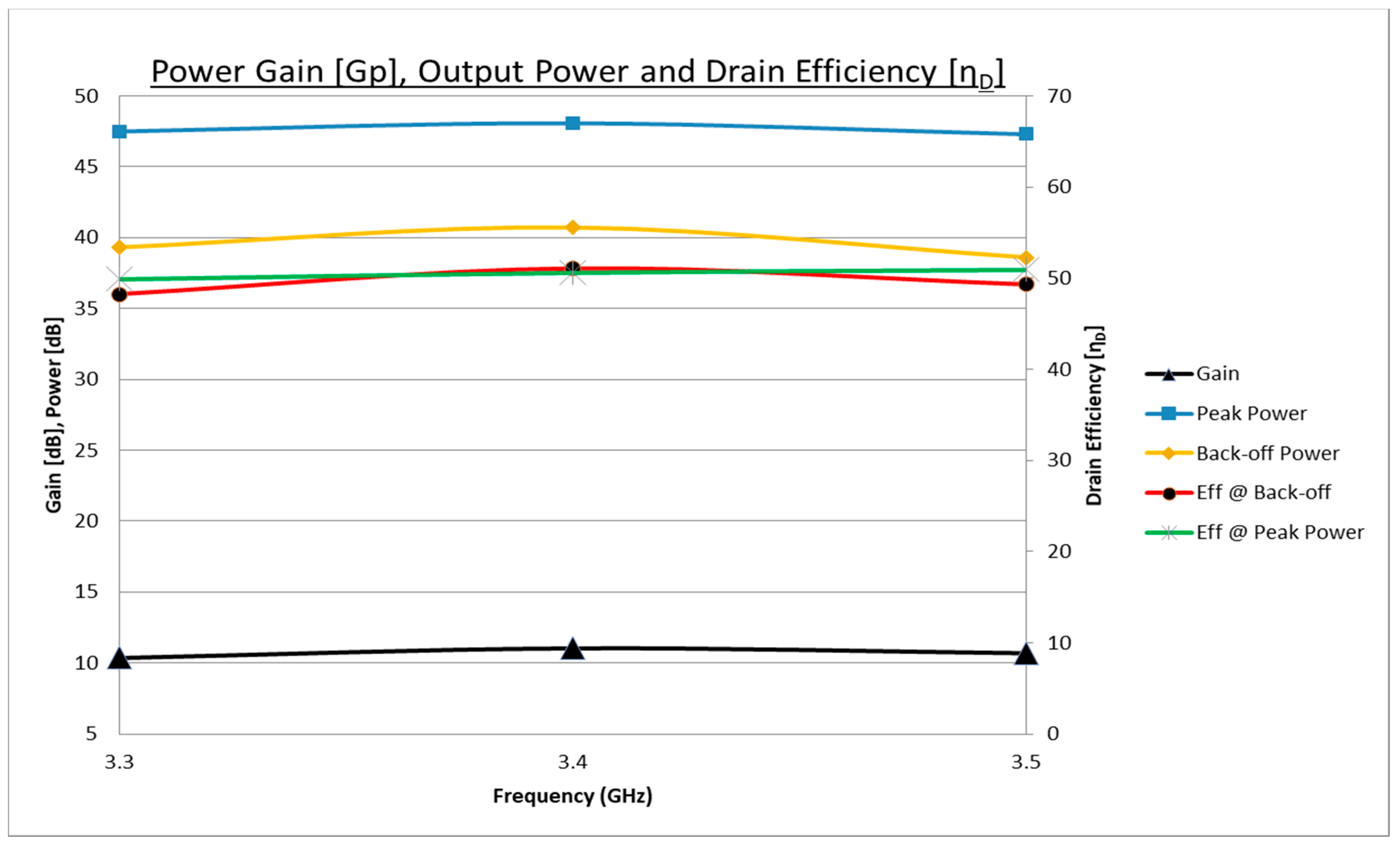
The measured performance of the designed Doherty power amplifier is shown in
Figure 12 and
Figure 13, where the designed amplifier achieved about 8 dB output back-off with an average efficiency of 50% at that region. Hence, it can be noticed that the total output power is increased by the current injected by the auxiliary amplifier. At the same time, the total gain of the Doherty amplifier is lower than the single ended amplifier due to the effect of the input splitter, and the fact that the peaking amplifier is OFF.
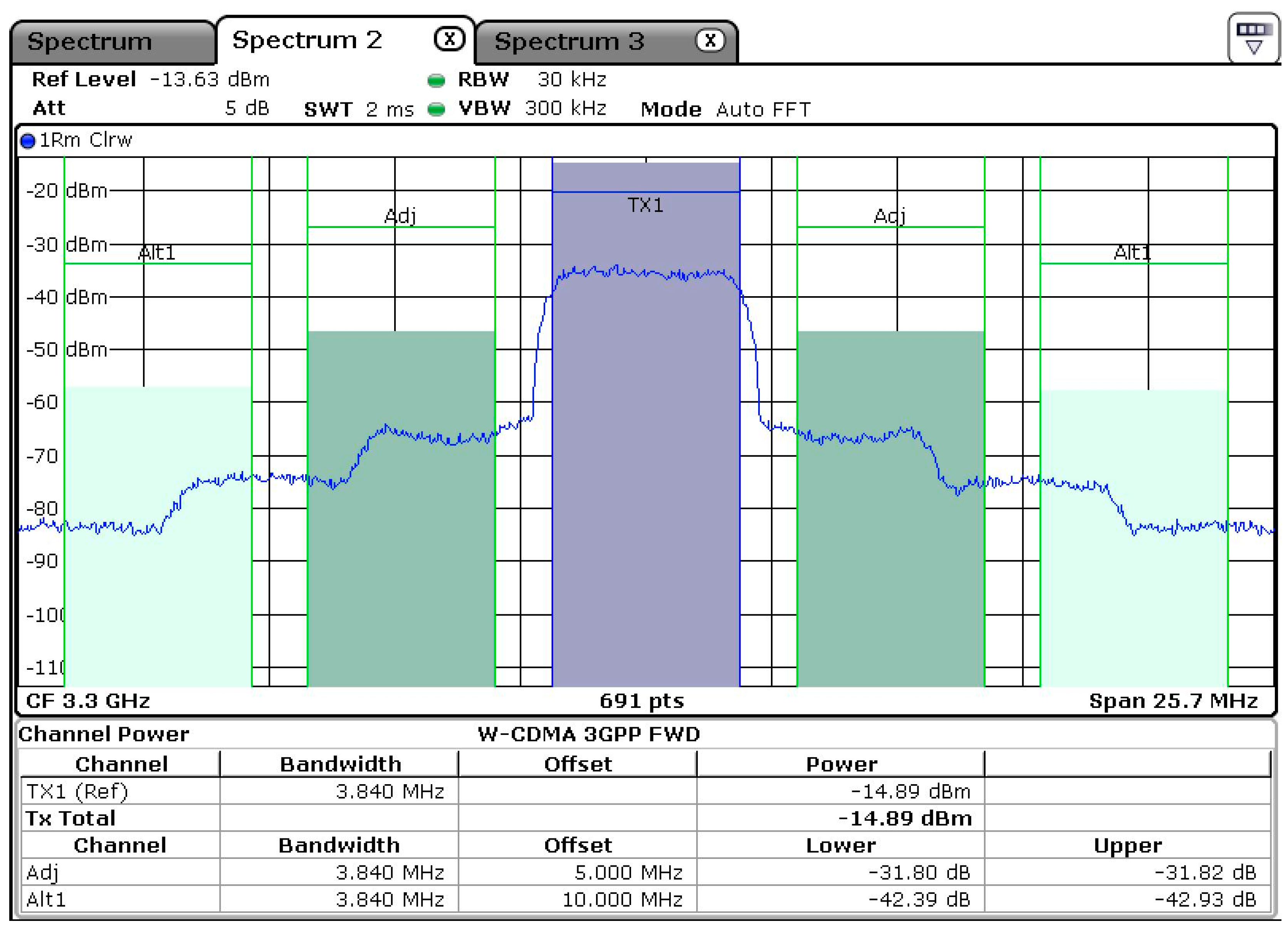
In terms of linearity,
Figure 14 shows the designed Doherty output spectrum when a modulated signal with 8 dB PAPR is applied. The average output of the PA was 40 dBm and the efficiency achieved was 50%. It can be noticed that the Adjacent Channel Power Ratio (ACPR) is 31.8 dB which can be corrected by a pre-distorter in order to satisfy the communications systems specifications. The linearization performance of the pre-distorter depends on the transistor nonlinear parameters such as the AM/PM response and the memory effect. A good indication of reducing the memory effect is the symmetry performance of the adjacent channels. The achieved results, compared with other works over the same frequency band, are presented in
Table 1.
5. Conclusions
The simplest way of providing a good efficiency at the output back-off region is the Doherty power amplifier, which depends on the load modulation at the summing point, where there are no additional circuits required. The simulated and measured performance of the asymmetrical Doherty amplifier was shown; an 8 dB OBO, with 40 dBm average power at 3.3–3.5 GHz was achieved. The Doherty power amplifier suffers from a lower gain due to the off state of the peaking amplifier and the input power splitter which reduces the input power level. The offset lines are needed for compensating the impedances and adjusting the phase difference between the two cells. The gain phase measurement provides a good indication about the power combination between the two amplifiers at the summing point, where the load modulation occurs. The average measured Doherty gain was 10 dB whereas, at the back-off point, the drain efficiency was 50%. Good linearity has been achieved when the designed amplifier was tested with 8 dB PAPR signal, and the average output was 40 dBm, which can be linearized.
Author Contributions
Conceptualization, A.M.A. and M.A.Y.; methodology, A.M.A., N.M. and M.A.Y.; software, A.M.A., R.A.A.-A. and M.A.Y.; validation, A.M.A., R.A.A.-A., N.M. and A.R.; formal analysis, A.M.A., R.A.A.-A., J.N., N.M., N.O.P., Y.I.A.A.-Y. and A.R.; investigation, A.M.A., M.A.Y., R.A.A.-A., J.N., N.M., N.O.P., Y.I.A.A.-Y. and A.R.; resources, A.M.A., M.A.Y., R.A.A.-A., J.N. and Y.I.A.A.-Y.; data curation, A.M.A., M.A.Y. and R.A.A.-A.; writing—original draft preparation, A.M.A., M.A.Y. and R.A.A.-A.; writing—review and editing, A.M.A., M.A.Y., J.N. and R.A.A.-A.; visualization, A.M.A., M.A.Y., R.A.A.-A. and J.N.
Funding
This project has received funding from the European Union’s Horizon 2020 research and innovation programme under grant agreement H2020-MSCA-ITN-2016 SECRET-722424.
Acknowledgments
The authors wish to express their thanks for the support provided by the innovation programme under grant agreement H2020-MSCA-ITN-2016 SECRET-722424.
Conflicts of Interest
The authors declare no conflict of interest.
References
- Cripps, S.C. RF Power Amplifiers for Wireless Communications; Artech House: Norwood, MA, USA, 2006. [Google Scholar]
- Camarchia, V.; Pirola, M.; Quaglia, R.; Jee, S.; Cho, Y.; Kim, B. The Doherty Power Amplifier: Review of Recent Solutions and Trends. IEEE Trans. Microw. Theory Tech. 2015, 63, 559–571. [Google Scholar] [CrossRef] [Green Version]
- Abdulkhaleq, A.M.; Yahya, M.A.; Brunning, J.; Al-Yasir, Y.; Ojaroudi Parchin, N.; Rayit, A.; Abd-Alhameed, R.A.; Noras, J. Load-Modulation Technique for Next Generation Mobile. In Proceedings of the 2nd SECRET Workshop—Secure Network Coding for Reduced Energy next Generation Mobile Small Cells, IEEE 5G World Forum, Dresden, Germany, 30 September–2 October 2019. [Google Scholar]
- Doherty, W.H. A new high-efficiency power amplifier for modulated waves. Bell Syst. Tech. J. 1936, 15, 469–475. [Google Scholar] [CrossRef]
- Abdulkhaleq, A.M.; Yahya, M.A.; Ojaroudi Parchin, N.; Al-Yasir, Y.; Sajedin, M.; Rayit, A.; Elfergani, I.T.E.; Abd-Alhameed, R.A.; Rodriguez, J. 18-W Three-Way Doherty Amplifier for 5G Applications. In Proceedings of the Antennas and Propagation Conference, Birmingham, UK, 11–12 November 2019. [Google Scholar]
- Kim, H.; Seo, C. Improvement of Power Added Efficiency and Linearity in Doherty Amplifier using Dual Bias Control and Photonic Band-Gap Structure. In Proceedings of the 2007 Asia-Pacific Microwave Conference, Bangkok, Thailand, 11–14 December 2007; pp. 1–4. [Google Scholar]
- Abdulkhaleq, A.M.; Al-Yasir, Y.; Ojaroudi Parchin, N.; Brunning, J.; McEwan, N.; Rayit, A.; Abd-Alhameed, R.A.; Noras, J.; Abduljabbar, N. A 70-W Asymmetrical Doherty Power Amplifier for 5G Base Stations. In Proceedings of the Broadband Communications, Networks, and Systems, Cham, Faro, Portugal, 19–20 September 2019; pp. 446–454. [Google Scholar]
- Li, X.; Chen, W.; Zhang, Z.; Feng, Z.; Tang, X.; Mouthaan, K. A Concurrent Dual-Band Doherty pOwer Amplifier. In Proceedings of the 2010 Asia-Pacific Microwave Conference, Yokohama, Japan, 7–10 December 2010; pp. 654–657. [Google Scholar]
- Abdulkhaleq, A.M.; Yahya, M.A.; McEwan, N.; Rayit, A.; Abd-Alhameed, R.A.; Ojaroudi Parchin, N.; Al-Yasir, I.Y.; Noras, J. Recent Developments of Dual-Band Doherty Power Amplifiers for Upcoming Mobile Communications Systems. Electronics 2019, 8, 638. [Google Scholar] [CrossRef]
- Barakat, A.; Thian, M.; Fusco, V.; Bulja, S.; Guan, L. Toward a More Generalized Doherty Power Amplifier Design for Broadband Operation. IEEE Trans. Microw. Theory Tech. 2017, 65, 846–859. [Google Scholar] [CrossRef]
- Rubio, J.M.; Fang, J.; Camarchia, V.; Quaglia, R.; Pirola, M.; Ghione, G. 3–3.6-GHz Wideband GaN Doherty Power Amplifier Exploiting Output Compensation Stages. IEEE Trans. Microw. Theory Tech. 2012, 60, 2543–2548. [Google Scholar] [CrossRef]
- Kosaka, N.; Fujiwara, S.; Okamura, A.; Chomei, K.; Sasaki, Y.; Horiguchi, K.; Katayama, H.; Inoue, A. A High-Efficiency and High-Gain, Plastic Packaged GaN HEMT for 3.5-GHz-band LTE Base Stations. In Proceedings of the IEEE International Symposium on Radio-Frequency Integration Technology (RFIT), Taipei, Taiwan, 24–26 August 2016; pp. 1–3. [Google Scholar]
- Huang, C.; He, S.; Dai, Z.; Pang, J.; Hu, Z.B. A 80W High Gain and Broadband Doherty Power Amplifier for 4/5G Wireless Communication Systems. In Proceedings of the 2016 IEEE MTT-S International Microwave Symposium (IMS), San Francisco, CA, USA, 22–27 May 2016; pp. 1–4. [Google Scholar]
- Xiong, H.; Chen, W.; Chen, L.; Chen, X.; Feng, Z. A High Efficiency Asymmetric Doherty Power Amplifier Using Symmetric Devices for 5G Application. In Proceedings of the 2018 International Conference on Microwave and Millimeter Wave Technology (ICMMT), Chengdu, China, 7–11 May 2018; pp. 1–3. [Google Scholar]
© 2019 by the authors. Licensee MDPI, Basel, Switzerland. This article is an open access article distributed under the terms and conditions of the Creative Commons Attribution (CC BY) license (http://creativecommons.org/licenses/by/4.0/).

 ,
, 


