An Efficient and Low-Power Design of the SM3 Hash Algorithm for IoT

 , ,
, ,
Abstract
1. Introduction
- New overall implementation architecture is proposed, which includes the embedded CPU, AHB-SIC, the SM3 circuit module and other modules. The AHB-SIC is designed to easily convert SM3 modules with the non-standard interface into the standard AHB slave interface. The SM3 circuit module is implemented by the software/hardware co-design method to enhance flexibility and reduce the hardware resource.
- Task scheduling and hardware resource optimization methods are applied in the expansion process to reduce the hardware area and power consumption so as to improve overall performance of SM3 implementation. The task scheduling and critical path optimization techniques are also applied in compression module design to reduce time delay and improve efficiency. The identical controller is shared in both expansion and compression modules to simplify the control circuit and reduce the hardware overheads.
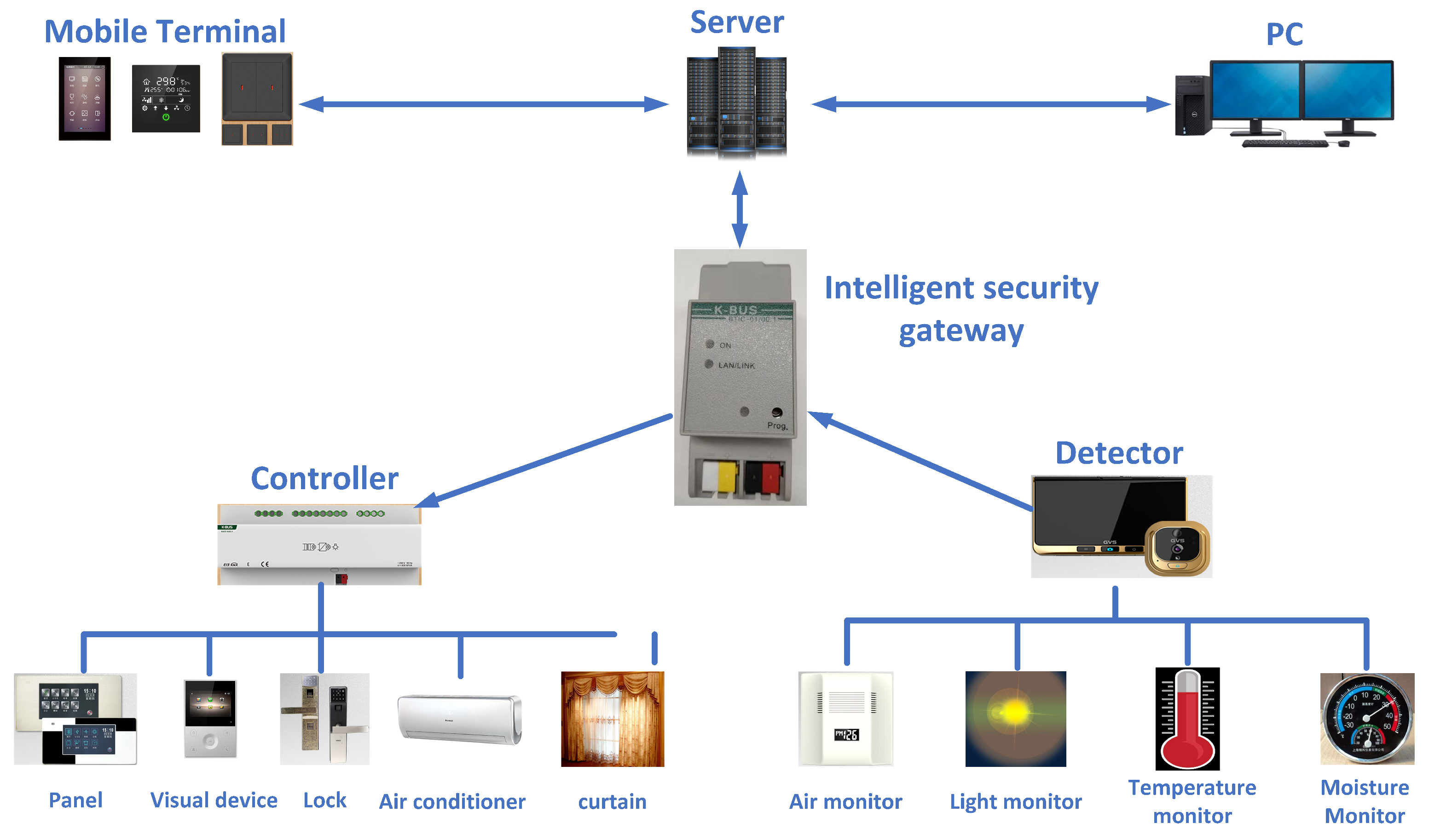
- The proposed architecture is implemented on FPGA and ASIC, and also applied to an intelligent gateway. Combined with the other cryptographic modules, our proposed SM3 module can realize the digital signature and identity authentication to protect the security of user data. This framework can also be integrated into other IoT devices.
2. SM3 Background
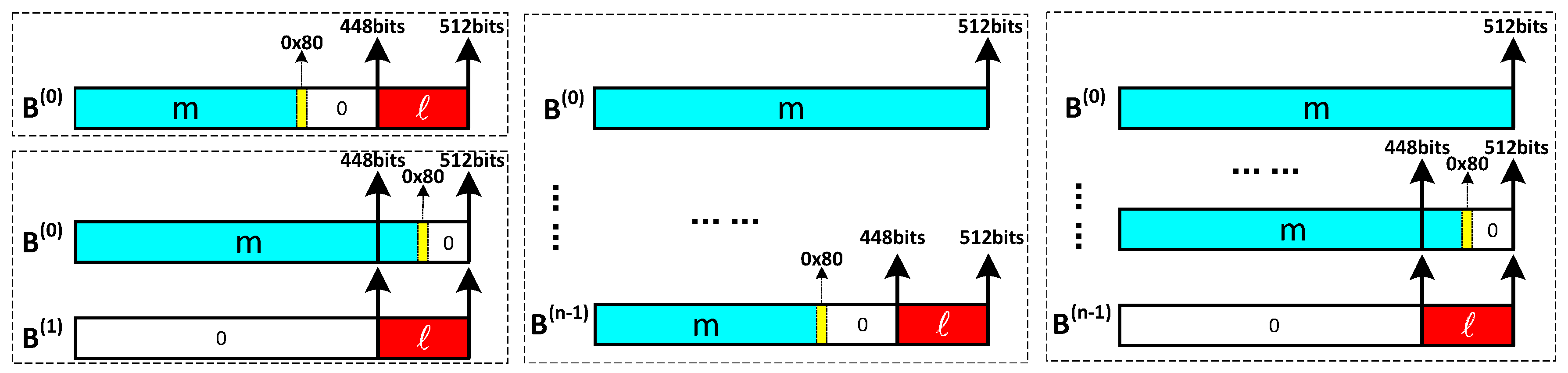
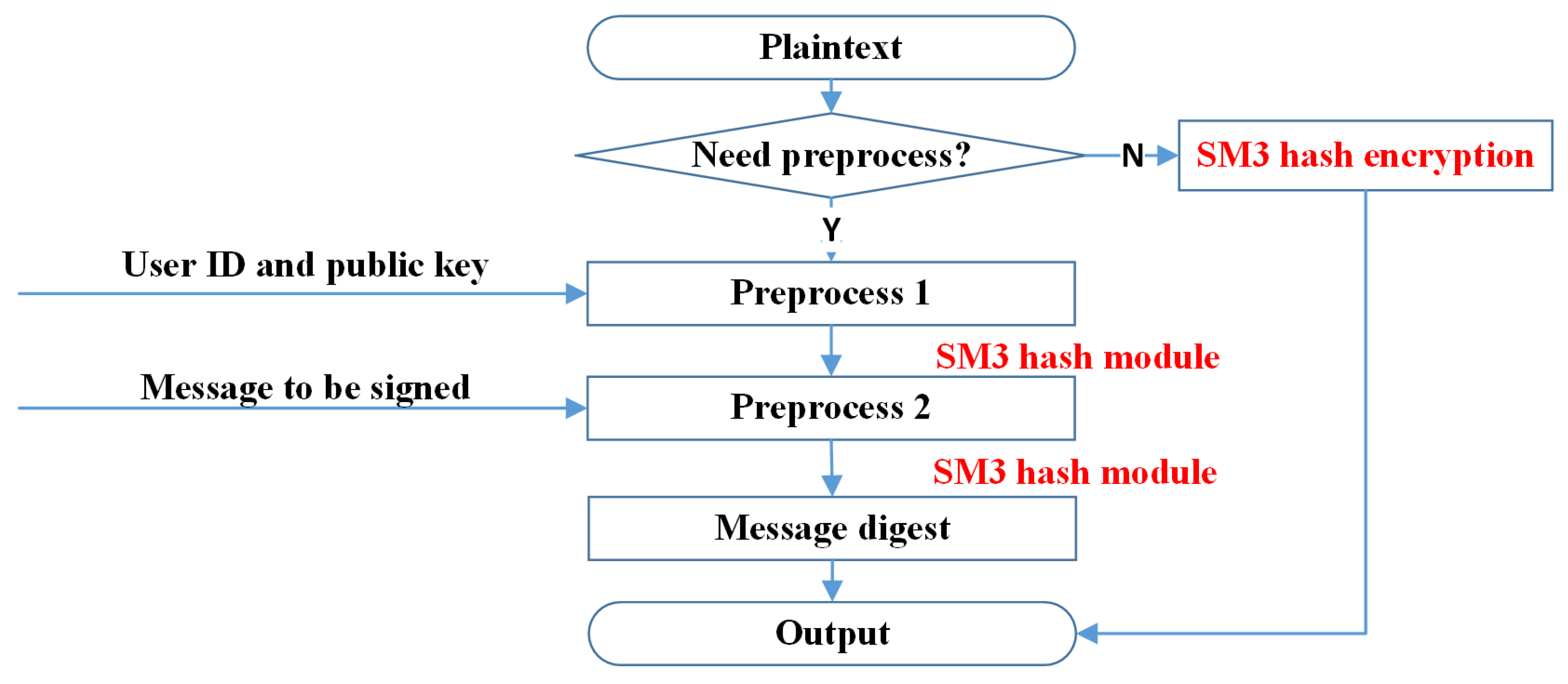
2.1. Padding and Parsing
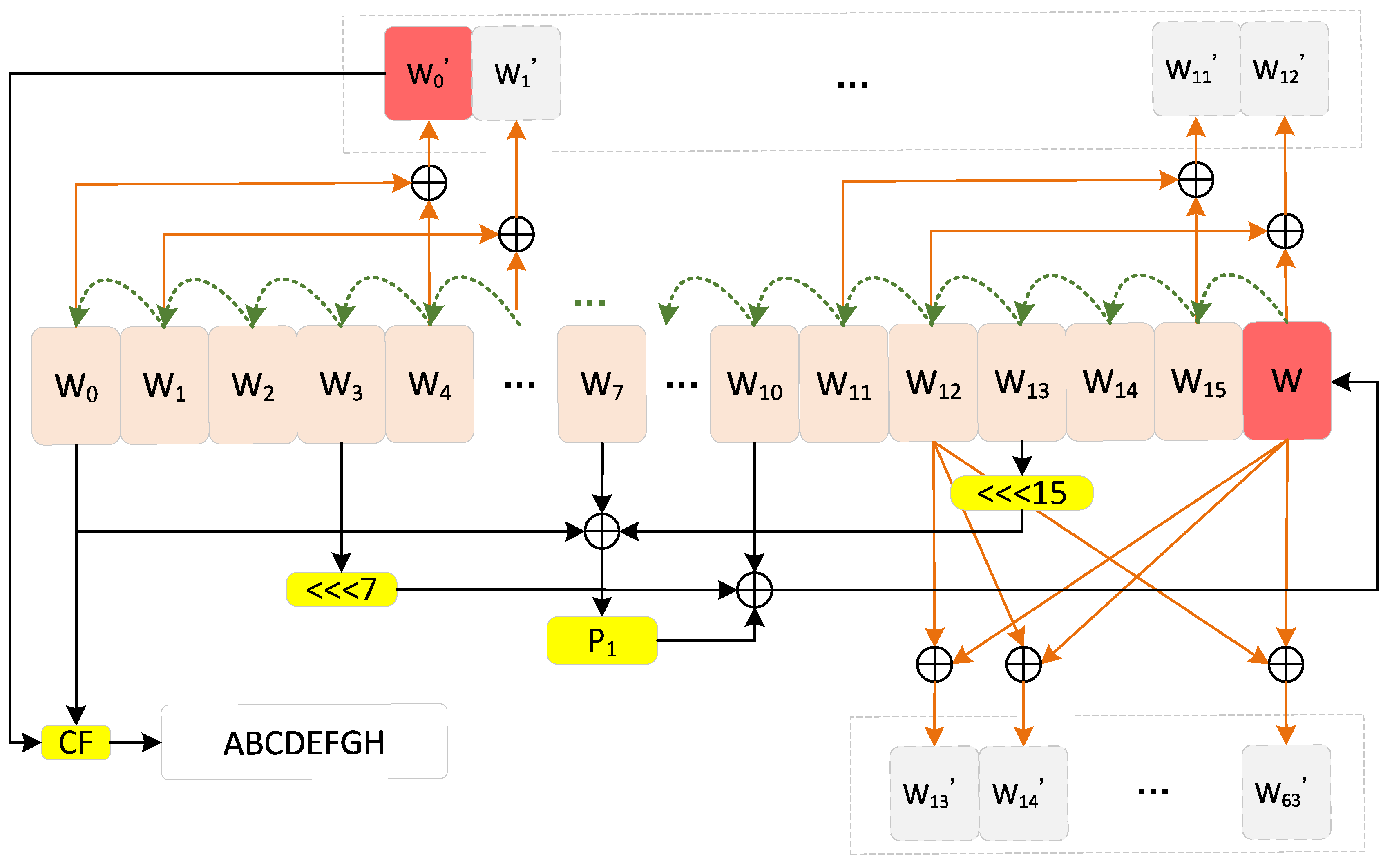
2.2. Expansion
- Divide the message into 16 words . The size of each word is 32-bit.
- FOR to 67ENDFORIn the Equation (1), ⊕ and ⋘ represent the bitwise XOR and ROL operations, respectively; is the permutation function.
- FOR to 63ENDFOR
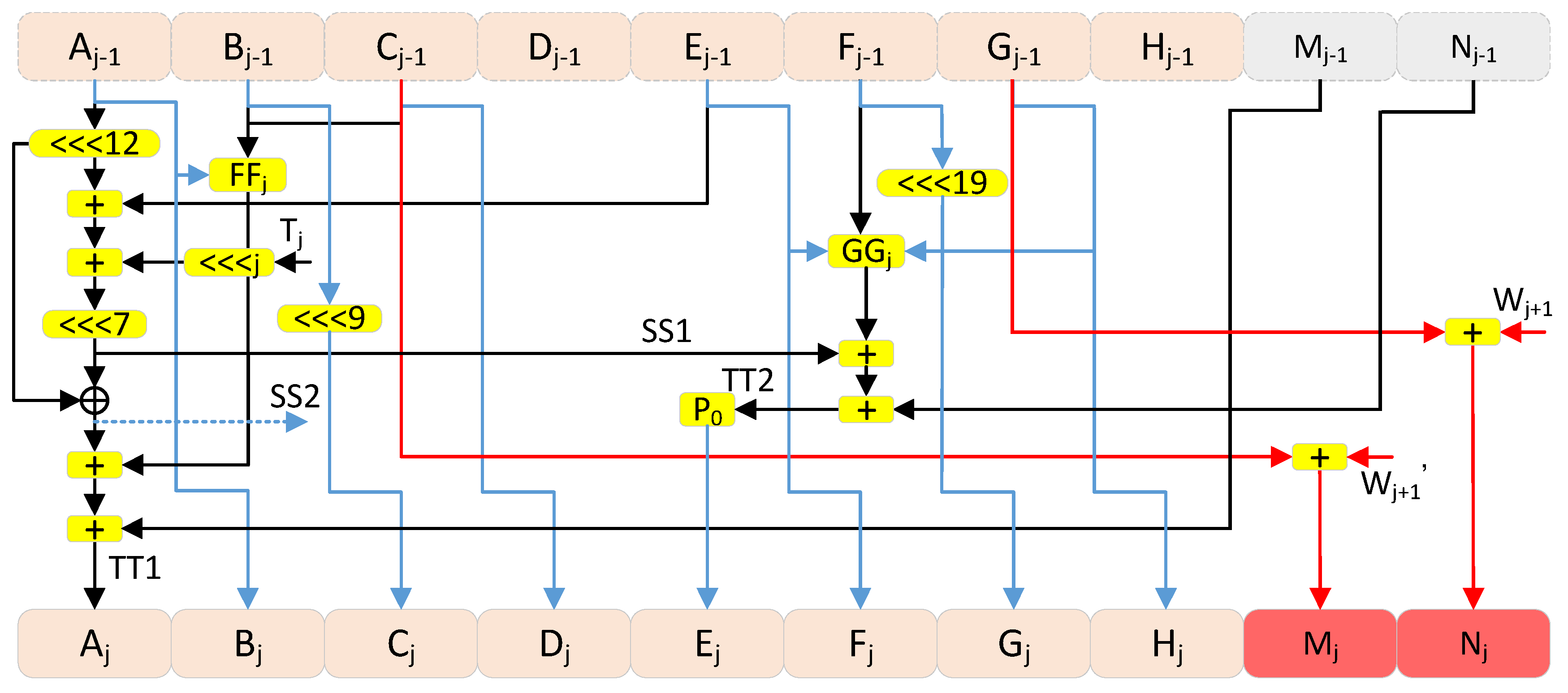
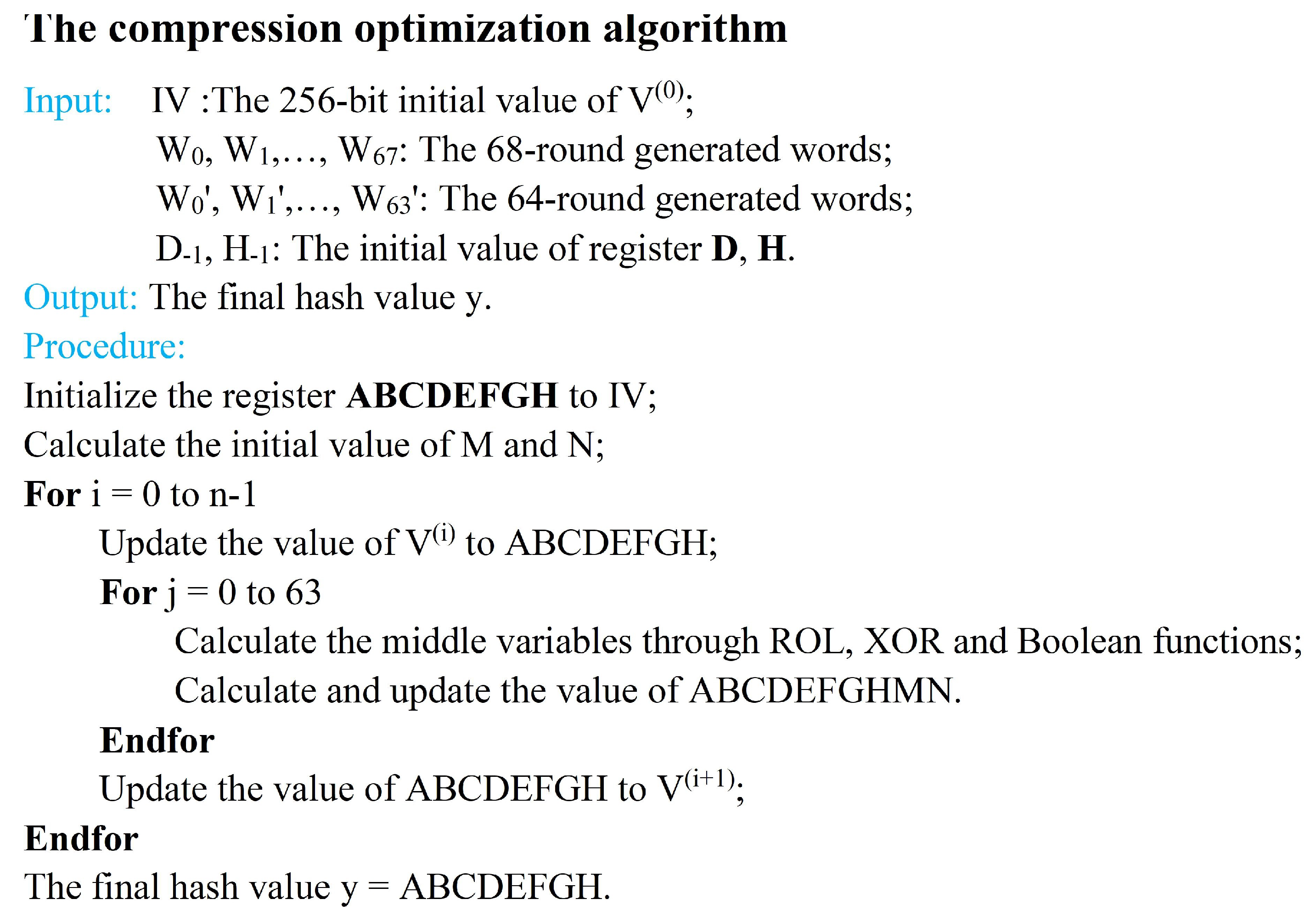
2.3. Compression
3. Proposed Architecture
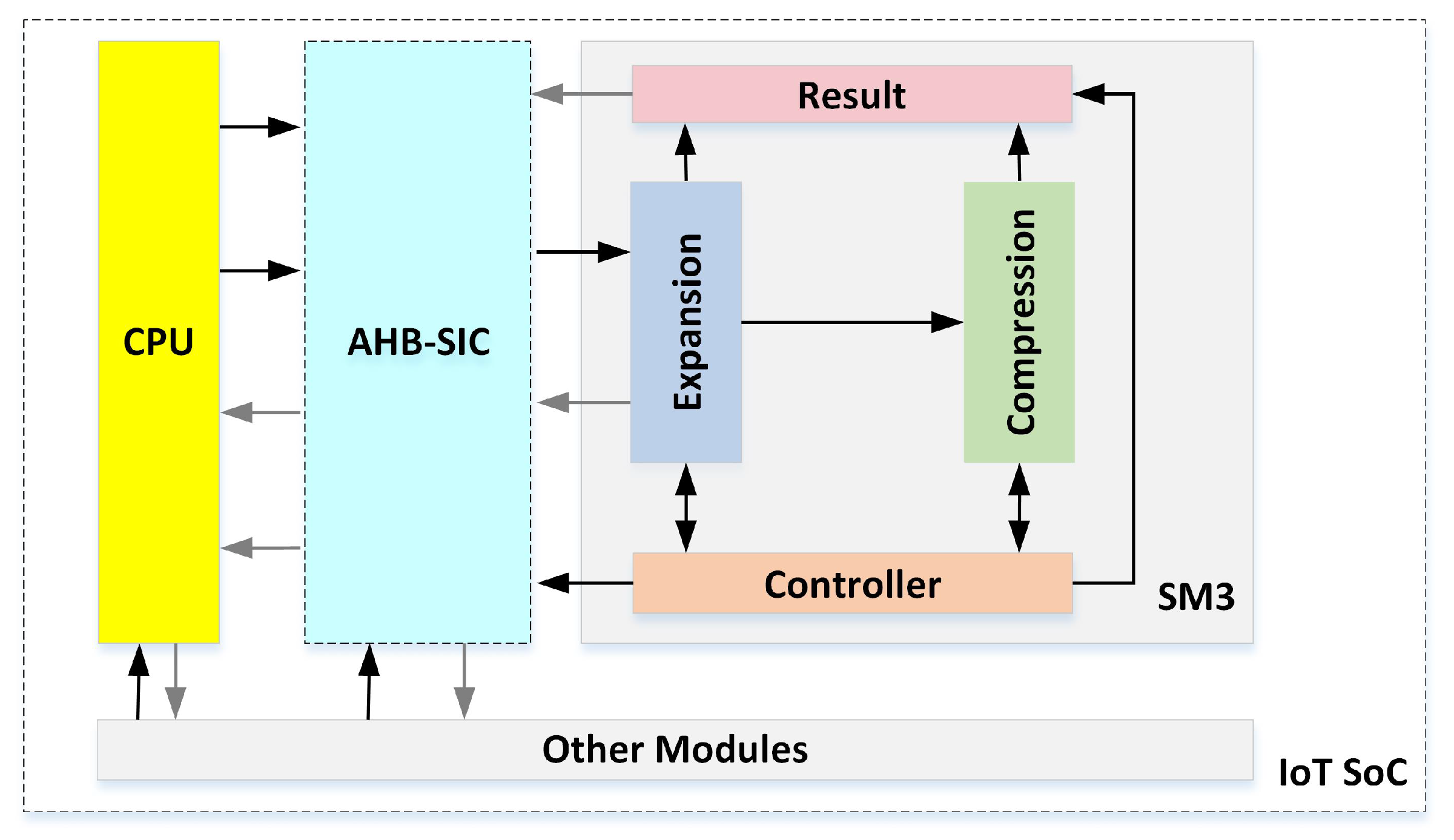
3.1. Overall Implementation Architecture
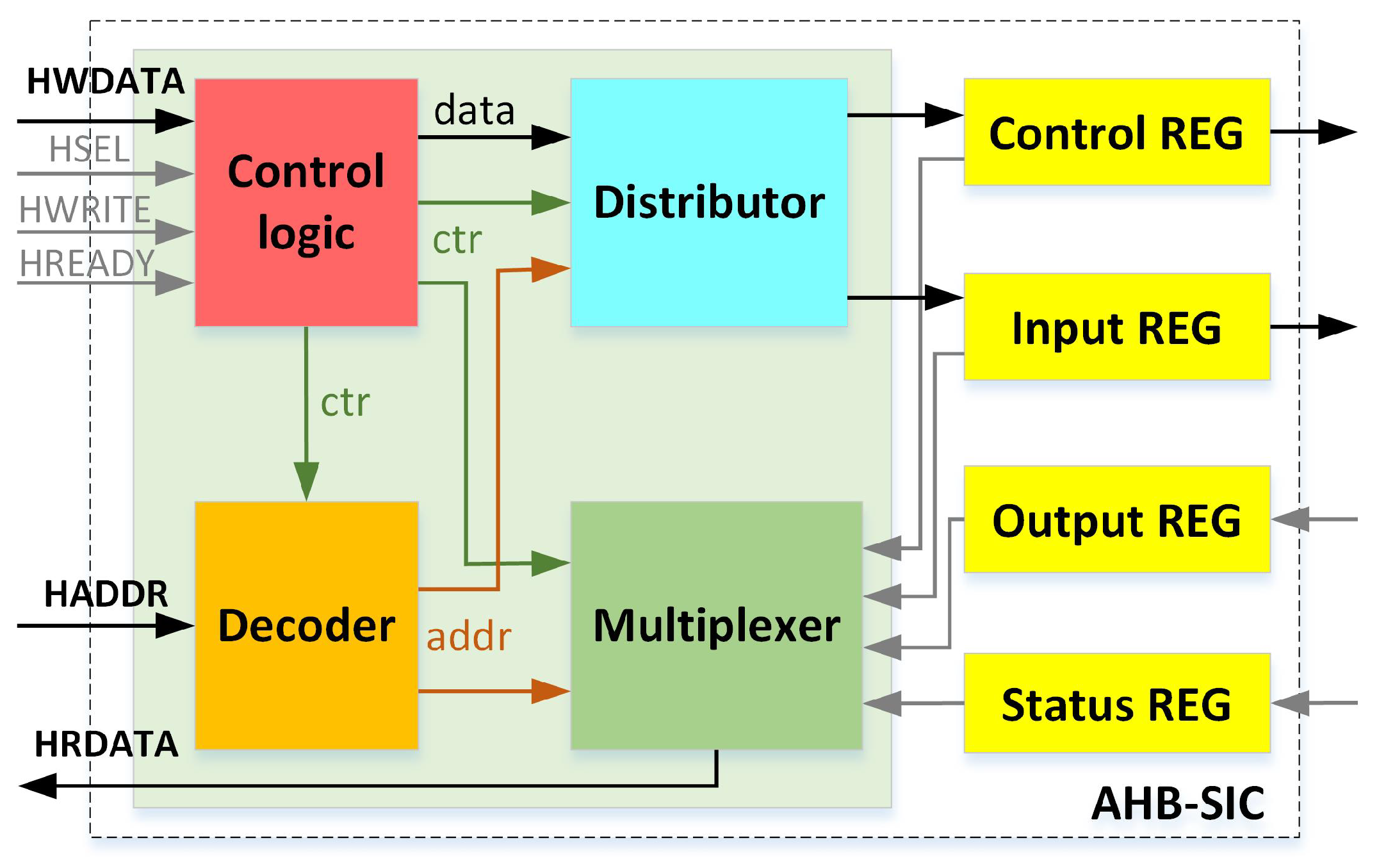
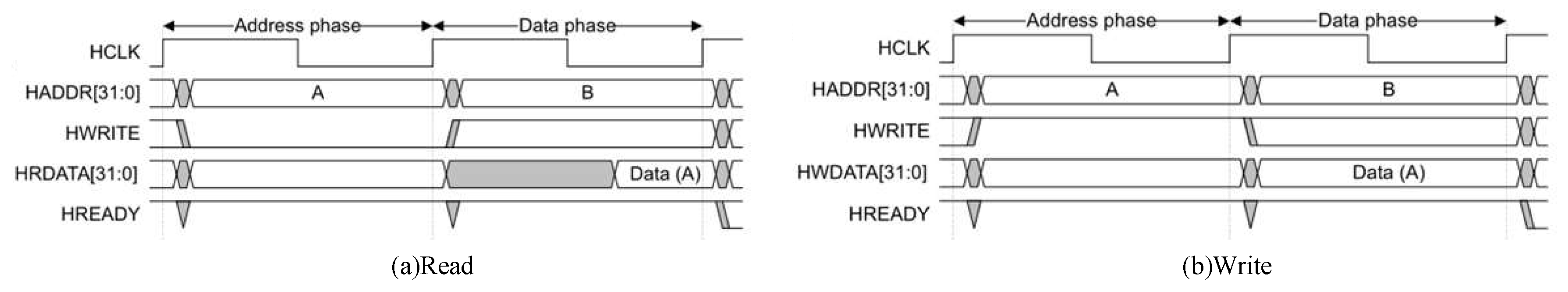
3.2. The AHB-SM3 Interface Controller
3.3. SM3 Implementation
3.3.1. Software/Hardware Co-Design
3.3.2. Controller Design
3.3.3. Expansion Module Design
3.3.4. Compression Module Design
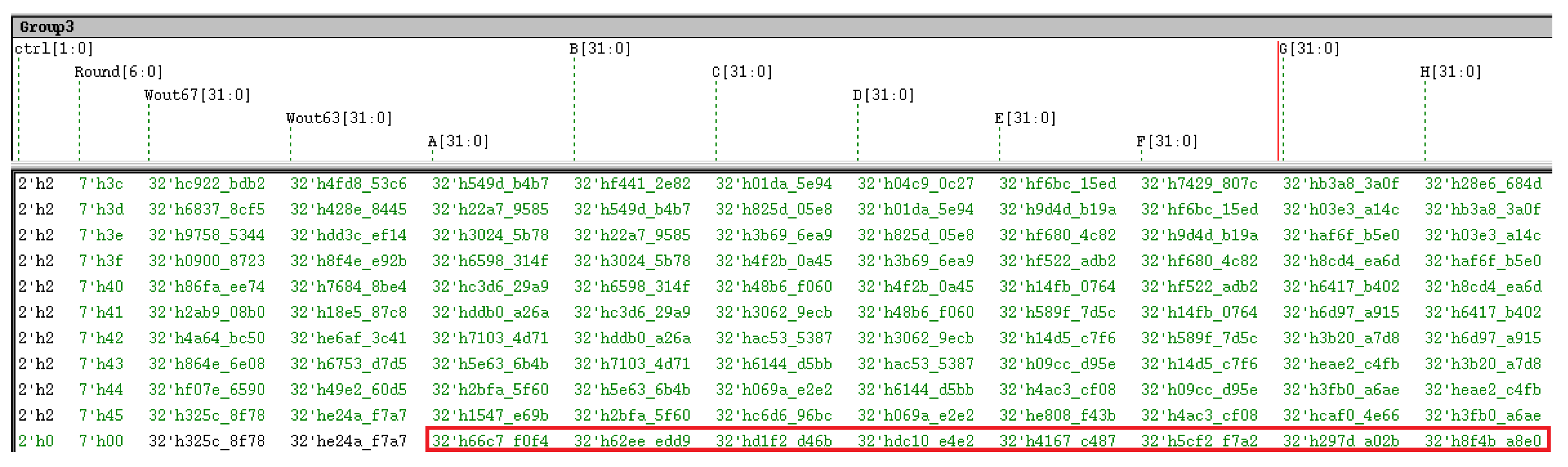
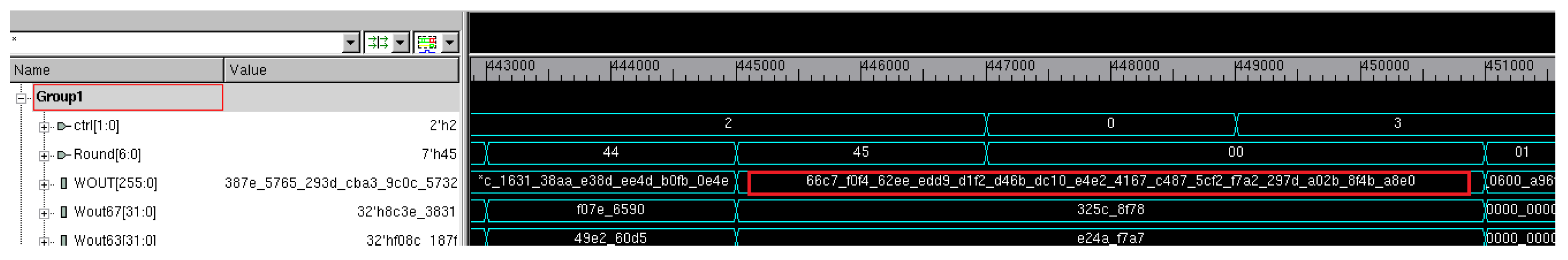
4. Analysis and the Experiment Result
4.1. The Setting and Implementation of the Experiment
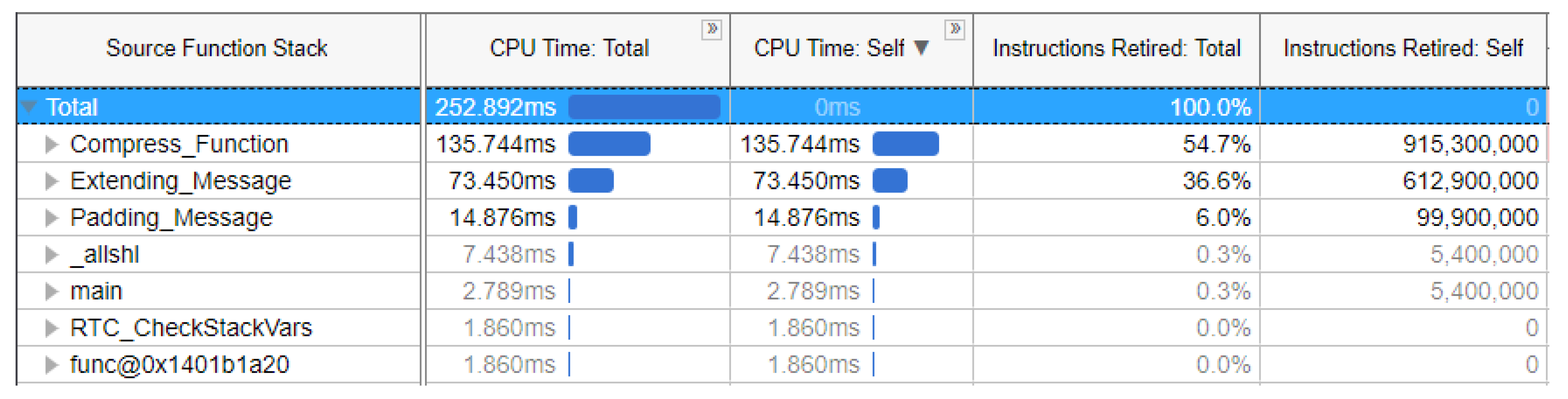
4.2. Time and Resource Consumption Analysis
4.3. Computation Amount Analysis
4.4. Comparison with Pure Software
4.5. Comparison with Other Related Work
5. An Example of IoT Application of SM3
6. Conclusions
Author Contributions
Funding
Conflicts of Interest
References
- Zhou, J.; Cao, Z.; Dong, X.; Vasilakos, A.V. Security and privacy for cloud-based IoT: Challenges. IEEE Commun. Mag. 2017, 55, 26–33. [Google Scholar] [CrossRef]
- Surendran, S.; Nassef, A.; Beheshti, B.D. A survey of cryptographic algorithms for IoT devices. In Proceedings of the 2018 IEEE Long Island Systems, Applications and Technology Conference (LISAT), Bahawalpur, Pakistan, 23–25 October 2018; pp. 1–8. [Google Scholar]
- Hwang, Y.H. IoT Security and Privacy: Threats and Challenges. In Proceedings of the Acm Workshop on Iot Privac, Singapore, 14–17 April 2015. [Google Scholar]
- Zhou, W.; Jia, Y.; Peng, A.; Zhang, Y.; Liu, P. The Effect of IoT New Features on Security and Privacy: New Threats, Existing Solutions, and Challenges Yet to Be Solved. IEEE Internet Things J. 2018, 6, 1606–1616. [Google Scholar] [CrossRef]
- Davidson, D.; Moench, B.; Ristenpart, T.; Jha, S. FIE on firmware: finding vulnerabilities in embedded systems using symbolic execution. In Proceedings of the 22nd USENIX conference on Security, Washington, DC, USA, 14–16 August 2013. [Google Scholar]
- Tsiropoulou, E.E.; Baras, J.S.; Papavassiliou, S.; Qu, G. On the Mitigation of Interference Imposed by Intruders in Passive RFID Networks. In Decision and Game Theory for Security, Proceedings of the International Conference, New York, NY, USA, 2–4 November 2016; Springer: Berlin/Heidelberg, Germany, 2016. [Google Scholar]
- Shi, Y.; Wei, W.; He, Z.; Fan, H. An ultra-lightweight white-box encryption scheme for securing resource-constrained IoT devices. In Proceedings of the the 32nd Annual Conference, Los Angeles, CA, USA, 5–9 December 2016. [Google Scholar]
- Buchmann, J.; Göpfert, F.; Güneysu, T.; Oder, T.; Pöppelmann, T. High-performance and lightweight lattice-based public-key encryption. In Proceedings of the 2nd ACM International Workshop on IoT Privacy, Trust, and Security, Xi’an, China, 30 May–3 June 2016; pp. 2–9. [Google Scholar]
- Rajesh, S.; Paul, V.; Menon, V.G.; Khosravi, M.R. A secure and efficient lightweight symmetric encryption scheme for transfer of text files between embedded IoT devices. Symmetry 2019, 11, 293. [Google Scholar] [CrossRef]
- Yan, H.; Wang, Y.; Jia, C.; Li, J.; Xiang, Y.; Pedrycz, W. IoT-FBAC: Function-based access control scheme using identity-based encryption in IoT. Future Gener. Comput. Syst. 2019, 95, 344–353. [Google Scholar] [CrossRef]
- State Cryptography Administration of China. Specification of SM3 Cryptographic Hash Function; State Cryptography Administration of China: Beijing, China, 2010. [Google Scholar]
- Ao, T.; He, Z.; Rao, J.; Dai, K.; Zou, X. A compact hardware implementation of SM3 hash function. In Proceedings of the 2014 IEEE 13th International Conference on Trust, Security and Privacy in Computing and Communications, Beijing, China, 24–26 September 2014; pp. 846–850. [Google Scholar]
- Hu, Y.; Wu, L.; Wang, A.; Wang, B. Hardware design and implementation of SM3 hash algorithm for financial IC card. In Proceedings of the 2014 Tenth International Conference on Computational Intelligence and Security, Yunnan, China, 15–16 November 2014; pp. 514–518. [Google Scholar]
- Khan, A.; Ganesh, G.; Dhodapkar, S.D.; Biswas, B.B.; Patil, R.K. A cryptographic primitive based authentication scheme for run-time software of embedded systems. In Proceedings of the 2010 2nd International Conference on Reliability, Safety and Hazard-Risk-Based Technologies and Physics-of-Failure Methods (ICRESH), Mumbai, India, 14–16 December 2010; pp. 500–504. [Google Scholar]
- Juliato, M.; Gebotys, C.H. Tailoring a Reconfigurable Platform to SHA-256 and HMAC through Custom Instructions and Peripherals. In Proceedings of the International Conference on Reconfigurable Computing and Fpgas, Cancun, Mexico, 9–11 December 2009. [Google Scholar]
- Algredo-Badillo, I.; Feregrino-Uribe, C.; Cumplido, R.; Morales-Sandoval, M. FPGA-based implementation alternatives for the inner loop of the Secure Hash Algorithm SHA-256. Microprocess. Microsyst. 2013, 37, 750–757. [Google Scholar] [CrossRef]
- Federal Information Processing Standards Publication 180-2. Announcing the Secure Hash Standard; US DoC/NIST: Gaithersburg, MD, USA, 2002.
- “ISO/IEC 10118-3”, IT Security Techniques-Hash Functions-Part 3: Dedicated Hash Functions. Available online: https://www.iso.org/standard/67116.html (accessed on 7 July 2019).
- Preneel, B. Software performance of encryption algorithms and hash functions. In Proceedings of the Selected Areas in Cryptography Annual International Workshop Sac, Ottawa, Canada, 18–19 May 1995; pp. 89–98. [Google Scholar]
- Chen, D.; Li, Y.J. A High Throughput Rate SM3 IP Design and Implementation. Electron Devices 2017, 03, 622–625. [Google Scholar]
- Chen, P. Optimization Implementation of SM3 Algorithm Based on 64 Rounds Grading Calculation. In Proceedings of the IOP Conference Series: Earth and Environmental Science, Yuzhno-Sakhalinsk, Russia, 27–31 May 2019. [Google Scholar]
- Azeez, N.A.; Chinazo, O.J. Achieving Data Authentication with Hmac-Sha256 Algorithm. Comput. Sci. Telecommun. 2018, 54, 135–142. [Google Scholar]
- Shen, Y.; Bai, D.; Yu, H. Improved cryptanalysis of step-reduced SM3. Sci. China Inf. Sci. 2018, 61, 038105:1–038105:2. [Google Scholar] [CrossRef]
- Yu, Y.; Yan, Y.; Li, W. High Speed ASIC Design and Implementation of SM3 Algorithm. Microelectron. Comput. 2016, 33, 21–26. [Google Scholar]
- Zhou, W.; Wang, B.; Zhang, W. Research and application of SM3 hardware implementation. Electron. Meas. Technol. 2015, 38, 67–71. [Google Scholar]
- AMBA 5 AHB Protocol Specification; ARM Inc.: Cambridge, UK, 2015.
- Pandey, A.; Tesfay, D.; Jarso, E. Performance analysis of Intel Ivy Bridge and Intel Broadwell microarchitectures using Intel VTune amplifier software. In Proceedings of the 2018 2nd International Conference on Inventive Systems and Control (ICISC), Coimbatore, India, 19–20 January 2018; pp. 423–426. [Google Scholar]
- Mavridou, A.; Laszka, A. Designing secure ethereum smart contracts: A finite state machine based approach. arXiv 2017, arXiv:1711.09327. [Google Scholar]
- McEvoy, R.P.; Crowe, F.M.; Murphy, C.C.; Marnane, W.P. Optimisation of the SHA-2 Family of Hash Functions on FPGAs. In Proceedings of the IEEE Computer Society Symposium on Emerging Vlsi Technologies and Architectures, Karlsruhe, Germany, 2–3 March 2006. [Google Scholar]
- Zhang, Y.; Xu, L.; Dong, Q.; Wang, J.; Blaauw, D.; Sylvester, D. ReCryptor: A Reconfigurable Cryptographic Cortex-M0 Processor With In-Memory and Near-Memory Computing for IoT Security. IEEE J. Solid-State Circuits 2018, 53, 995–1005. [Google Scholar] [CrossRef]
- Ma, Y.; Xia, L.; Lin, J.; Jing, J.; Liu, Z.; Yu, X. Hardware performance optimization and evaluation of SM3 hash algorithm on FPGA. In Proceedings of the International Conference on Information and Communications Security, Hong Kong, China, 29–31 October 2012; Springer: Berlin/Heidelberg, Germany, 2012; pp. 105–118. [Google Scholar]
- Cao, X.; Lu, L.; O’Neill, M. A compact SHA-256 architecture for RFID tags. In Proceedings of the 22nd IET Irish Signals and Systems Conference, Dublin, Ireland, 23–24 June 2011. [Google Scholar]
- He, Z.; Wu, L.; Zhang, X. High-speed Pipeline Design for HMAC of SHA-256 with Masking Scheme. In Proceedings of the 2018 12th IEEE International Conference on Anti-counterfeiting, Security, and Identification (ASID), Xiamen, China, 19–21 October 2018. [Google Scholar]
- Beuchat, J.L.; Okamoto, E.; Yamazaki, T. Compact implementations of BLAKE-32 and BLAKE-64 on FPGA. In Proceedings of the 2010 International Conference on Field-Programmable Technology, Beijing, China, 8–10 December 2010; pp. 170–177. [Google Scholar]
- Yin, Y.; Jiang, D. Research and Application on Intelligent Parking Solution Based on Internet of Things. In Proceedings of the 2013 5th International Conference on Intelligent Human-Machine Systems and Cybernetics, Hangzhou, China, 26–27 August 2013. [Google Scholar]
- Tsiropoulou, E.E.; Baras, J.S.; Papavassiliou, S.; Sinha, S. RFID-based smart parking management system. Cyber-Phys. Syst. 2017, 3, 22–41. [Google Scholar] [CrossRef]
- Pinto, A.; Costa, R. Hash-chain-based authentication for IoT. Adv. Distrib. Comput. Artif. Intell. J. 2016, 5, 43–57. [Google Scholar] [CrossRef]


| Algorithms | SHA-224 | SHA-256 | SHA-384 | SHA-512 | SHA3-224 | SHA3-256 | SHA3-384 | SHA3-512 | SM3 |
|---|---|---|---|---|---|---|---|---|---|
| Message size | < | < | < | < | − | − | − | − | < |
| Block size | 512 | 512 | 1024 | 1024 | 1152 | 1088 | 832 | 576 | 512 |
| Digest size | 224 | 256 | 384 | 512 | 224 | 256 | 384 | 512 | 256 |
| Security | 112 | 128 | 192 | 256 | 112 | 128 | 192 | 256 | 128 |
| Value Range | |||
|---|---|---|---|
| Operation | Clock Cycles | Register | Additions of the Critical Path | Slack |
|---|---|---|---|---|
| Non-optimized | 196 | 148 | 5 | 0.0 |
| Optimized | 70 | 36 | 4 | 1.31 |
| Operation | LOAD | STORE | XOR | LOAD | ADD | AND | OR | NOT | Total |
|---|---|---|---|---|---|---|---|---|---|
| Non-optimized | 596 | 900 | 632 | 720 | 512 | 240 | 144 | 48 | 3792 |
| Optimized | 400 | 192 | 632 | 528 | 512 | 240 | 144 | 48 | 2696 |
| Design | Platforms | Frequency (MHz) | Clock Cycles | Areas (Gates) | Power (mW) | Throughput (Mbps) |
|---|---|---|---|---|---|---|
| This work | 0.13-m | 36 | 70 | 6036 | 1.24 | 263 |
| SHA-3 [30] | 0.04-m | 28.8 | 3329 | 886 | 4.87 | 14 |
| SM3 [20] | 0.18-m | 200 | 1 | 8800k | - | 105k |
| SM3 [24] | 0.065-m | 526.3 | 80 | 5370 | - | 3368 |
| SM3 [12] | 0.13-m | 250 | 464 | 8277 | - | 276 |
| 0.13-m | 200 | 68 | 12,956 | - | 1506 | |
| SM3 [31] | 0.13-m | 216 | 68 | 9458 | - | 1619 |
| SHA-256 [32] | 0.13-m | 102 | 1120 | 9036 | 3.06 | 47 |
| Design | Platforms | Frequency (MHz) | Clock Cycles | Areas | Throughput (Mbps) |
|---|---|---|---|---|---|
| This work | Virtex-7 | 36 | 70 | 808 Slices | 263 |
| Virtex-7 | 50 | 70 | 808 Slices | 366 | |
| Virtex-7 | 100 | 70 | 808 Slices | 731 | |
| SHA-256 [33] | Cyclone II | 116.24 | 68 | 7219 Logic Cells | 875.22 |
| Cyclone II | 87.08 | 68 | 10,918 Logic Cells | 655.66 | |
| SM3 [25] | ZYNQ-7020 | 167.8 | 64 | 1743 Slices | 1342 |
| Standard-SM3 | Virtex-5 | 214 | 7.53 | 384 Slices | 1611 |
| C-SM3 | Virtex-5 | 215 | 7.53 | 234 Slices | 1619 |
| T-SM3 [31] | Virtex-5 | 362 | 7.53 | 328 Slices | 2726 |
| SHA-3 [34] | Virtex-5 | 372 | 846 | 56 Slices + 2 BRAM | 225 |
© 2019 by the authors. Licensee MDPI, Basel, Switzerland. This article is an open access article distributed under the terms and conditions of the Creative Commons Attribution (CC BY) license (http://creativecommons.org/licenses/by/4.0/).
Share and Cite
Zheng, X.; Hu, X.; Zhang, J.; Yang, J.; Cai, S.; Xiong, X. An Efficient and Low-Power Design of the SM3 Hash Algorithm for IoT. Electronics 2019, 8, 1033. https://doi.org/10.3390/electronics8091033
Zheng X, Hu X, Zhang J, Yang J, Cai S, Xiong X. An Efficient and Low-Power Design of the SM3 Hash Algorithm for IoT. Electronics. 2019; 8(9):1033. https://doi.org/10.3390/electronics8091033
Chicago/Turabian StyleZheng, Xin, Xianghong Hu, Jinglong Zhang, Jian Yang, Shuting Cai, and Xiaoming Xiong. 2019. "An Efficient and Low-Power Design of the SM3 Hash Algorithm for IoT" Electronics 8, no. 9: 1033. https://doi.org/10.3390/electronics8091033
APA StyleZheng, X., Hu, X., Zhang, J., Yang, J., Cai, S., & Xiong, X. (2019). An Efficient and Low-Power Design of the SM3 Hash Algorithm for IoT. Electronics, 8(9), 1033. https://doi.org/10.3390/electronics8091033