A Parametric Conducted Emission Modeling Method of a Switching Model Power Supply (SMPS) Chip by a Developed Vector Fitting Algorithm


School of Electronic and Information Engineering, Beihang University, Beijing 100083, China
*
Author to whom correspondence should be addressed.
Electronics 2019, 8(7), 725; https://doi.org/10.3390/electronics8070725
Submission received: 21 May 2019
/
Revised: 19 June 2019
/
Accepted: 23 June 2019
/
Published: 26 June 2019
(This article belongs to the Special Issue Power Converters in Power Electronics)
Abstract
:This paper proposes a modeling method to establish a parametric-conducted emission model of a switching model power supply (SMPS) chip through a developed vector fitting algorithm. A common SMPS chip LTM8025 was taken as an example to explain the modeling process. According to the integrated circuit (IC) electromagnetic modeling (ICEM) standard, the parametric conducted emission model is divided into two parts: IC internal activity (ICIA) and IC passive distribution network (ICPDN). The parameters of ICIA are identified by measured data and correlated with key components; an improved vector-fitting algorithm is proposed to solve the fitting problem of ICPDN without phase information. This parametric model can be used with commercial simulation software together to achieve predictions of conducted emissions from power modules. The experiment results show that the maximum and 90% confidence interval of the forecast errors are 9.677 dB and (−4.56 dB, 6.52 dB) respectively, which achieve the international standard requirements and have sufficient accuracy and effectiveness.
1. Introduction
Electromagnetic compatibility (EMC) is one of the important conditions for measuring the electromagnetic strength of a device or a system. With an increasing number of electronic and electric devices integrated into complex electronic information systems, the electromagnetic environments, including the circuit principle and the coupling relationship are increasingly complicated. The inside or outside electromagnetic interference (EMI) of the system leads to an increase in cases where the sensitive devices may become degraded or even unable to work properly.
In order to solve this problem, in the actual development process, the iterative process of ‘design-test-redesign’ has been carried out to ensure electromagnetic compatibility of the electronic and electric devices and complex information systems. To reduce the development period and cost, it is particularly important to make a reasonable prediction of its EMC before the prototype is produced. The importance of EMC design work has become increasingly prominent.
As a large number of devices are integrated into complex systems, switching model power supply (SMPS) becomes essential for its role in improving power efficiency and reducing costs. However, its rapid on-off and parasitic effects may lead to serious electromagnetic emission problems. This makes it difficult to pass the appropriate industrial EMC/EMI control standards and may affect the functional ability of itself or other equipment. To ensure electromagnetic compatibility of an equipment or system, electromagnetic (EM) emission prediction is required [1,2,3]. EM emission can be further categorized into conducted emission (CE) and radiated emission (RE). Since the switching frequency of SMPS is between several tens of kHz to serval MHz, the emission of SMPS is mainly transmitted by conduction.
For the conducted emission modeling of SMPS, the earlier research starts from the physical parameters of the device and constructs the CE model [4,5,6,7]. However, this method requires detailed information of the device, the modeling process is complicated, and the established model has poor precision. Another mainstream method is behavioral level modeling. This method directly establishes the CE model of SMPS for analysis without considering the specific parameters of the switching power supply. In terms of behavioral model construction, Norton or Thevenin equivalent can generally be used to give an equivalent circuit of a CE model, and its parameters are determined by analysis or test [8,9]. In addition to these two aspects, there are other methods for modeling SMPS, such as using a concept-named fast reconstruction method (FRM) to deal with the time domain simulation of common mode conducted disturbances [10].
The SMPS modeling methods mentioned above need to measure the properties of internal components so as to ensure the accuracy of the model. With the miniaturization of devices, an increasing number of SMPS chips have emerged. For SMPS chips, traditional CE modeling methods are no longer applicable because their components are packaged inside the chip and cannot be measured. To calculate the EM emission accurately, it is necessary to model SMPS at the chip-level through simulation and external measurement.
As for these matters, various research has been reported in the past years [11,12,13]. Reference [14] gives an overview of the EMC research focusing on chip-level. IBIS (I/O buffer information specification) model is the standard for electronic behavioral specifications for integrated circuit input/output analog characteristics [15]. However, it is not sufficient to directly apply EM emission modeling because the interference associated with the internal activities of the component is not considered. IMIC (I/O interface model for integrated circuits) model can effectively solve the modeling accuracy problem [16]. Considering the modeling process may require confidential information to build a netlist and read it through dedicated simulation software, the portability is not relatively high. ICEM (integrated circuit electromagnetic modeling) is a simple and intuitive method that uses RLC (resistance, inductance, and capacitance) circuits to fit the measured port characteristics, which seems accurate enough for EMC predictions [17,18].
In recent years, the ICEM method was widely used to model different integrated circuits (ICs) and predict their electromagnetic compatibility [19,20,21]. Jean-Luc Levant, et al. used the ICEM model to simulate and predict the jitter of the integrated phase-locked loop and provide a correction solution [22]. Hyun Ho Park, et al. generated a macro model of the timing controller chip for running pseudo H pattern data from transistor level simulation and is used to estimate the power switching current on the printed circuit board (PCB) [23]. Abhishek Ramanujan, et al. designed a common interchange format for ICEM based on the well-known extensible markup language format and applied to Atmega88 microcontrollers [13]. Modeling methods for PCB and components with both chips and packages were published in [24] and [25], in order to calculate PCB power noise generated by the switching chip.
Although the ICEM model has been successfully applied in many chip-level EM emission predictions, it still has certain limitations. In the modeling process, the ICEM model divides the IC model into the passive distribution network (PDN) component and the internal activity (IA) component [26]. The establishment of IA parameter extraction depends on the extracted PDN parameters and the measured external current, thus the parameters have no specific physical meaning and cannot be parametrically modeled based on different practical scenarios. Therefore, when application parameters are different from the test board, the accuracy of the predicted results will be limited as well. Su, D. et al. proposed a new theory named ‘basic emission waveform theory’, which characterizes emission with four basic waveforms by its physical characteristics of the equipment. The identification and analysis of an emission source can be realized by analyzing the basic waveforms from the emission of a complex system [27].
Based on the basic emission waveform theory, this paper proposes a parametric modeling method to establish the conducted emission model of an SMPS chip through a developed vector fitting algorithm.
The organization of this paper is as follows. Section 2 describes the measurement configuration required for modeling. Section 3 illustrates the model division and parametric modeling methods of each part. In Section 4, a set of comparative experiments and an application example are given to verify the effectiveness of the modeling method. Conclusions are drawn in Section 5 to summarize the work proposed.
2. Measurement Configuration
This study takes a commercial SMPS chip called LTM8025 [28] as an example to illustrate the modeling method. LTM8025 is a step down micro module converter chip and widely used in consumer electronics as power supply modules.
It usually requires a dedicated chip test board to predict its conducted emission by the ICEM method at chip-level modeling. However, since the output voltage and switching frequency of the LTM8025 are closely related to the selection of component parameters in the peripheral circuits, the user needs to make a particular measurement board according to the used parameters to ensure the modeling accuracy. Furthermore, when a power supply module needs to convert one input voltage into multiple different output voltages, the user needs to integrate multiple ICs on one PCB. Under this case, in order to accurately predict the conducted emission of the PCB, multiple measurement boards are required to build a variety of chip models under each working condition. This will undoubtedly lengthen the design process time and increase costs.
Instead of the particular measurement board in ICEM method, an official demonstration circuit DC1379B [29] of LTM8025 is used as the test board in this paper. Figure 1 shows the PCB and schematic of DC1379B. The authors measured the conducted emission currents of the port VIN (Power Input Port) and VOUT (Power Output Port) to extract the parametric model. As can be seen from Figure 1b, the port VIN provides a voltage input to the DC1379B, which is stepped down by the LTM8025 and filtered by the peripheral circuit, and is output from the port VOUT to the downstream load.
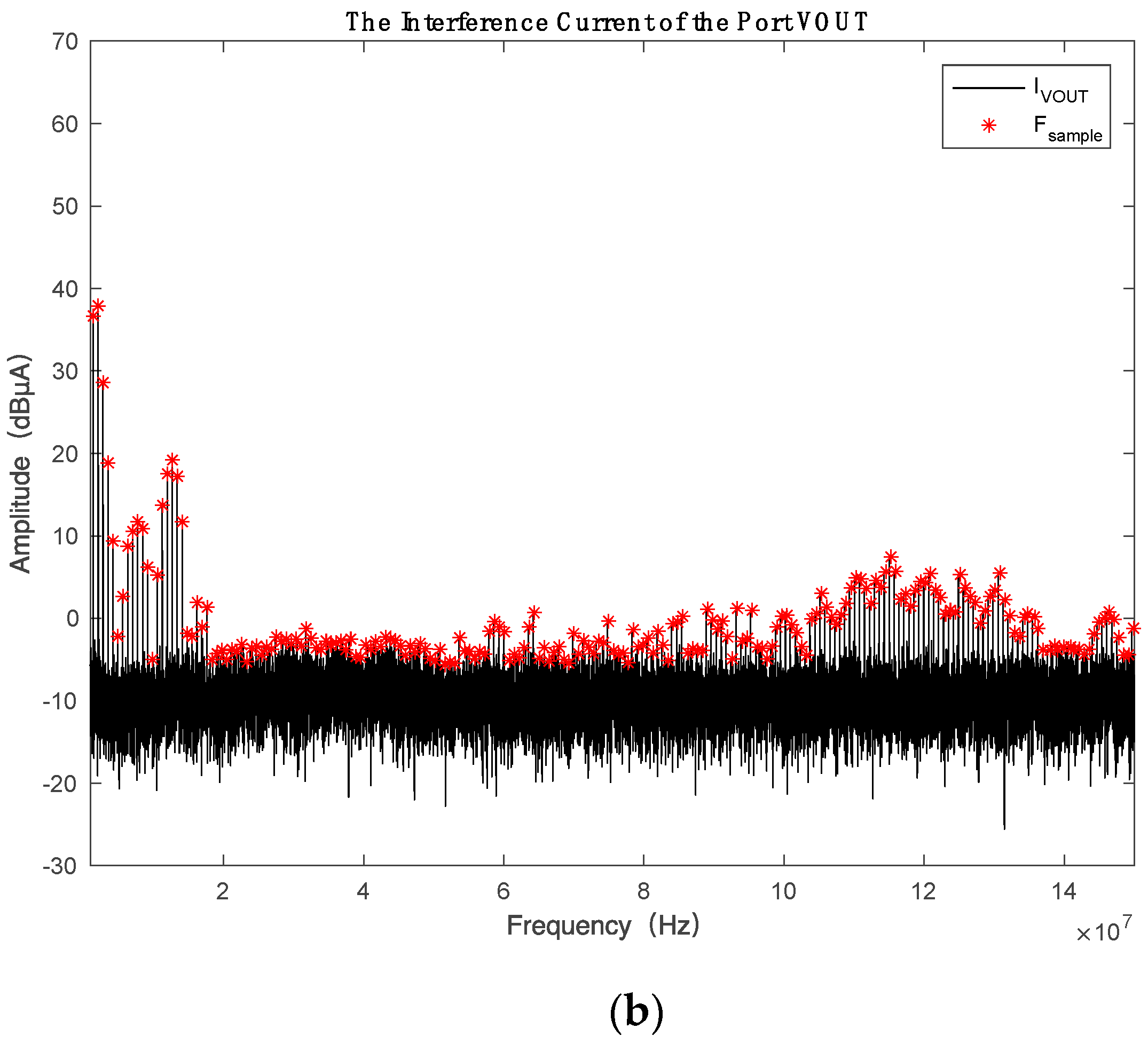
The experimental configuration during the measurement were as follows: The port VIN was connected to a stabilized DC voltage supply with an internal resistance of to provide a 30 V input voltage to the board; the port VOUT was connected with a high-power resistor as the downstream load; current monitor probe F-33-2 from the FCC company was used to connect to the spectrum analyzer to measure the conducted emission on the power lines (as shown in Figure 2). The measured results are shown in Figure 3.
3. Parametric Modeling Method
Referring to the ICEM partitioning method, the SMPS chip model is also divided into ICIA and ICPDN parts. Different from ICEM, based on the ‘basic emission waveform theory’, the authors treat ICIA as a square waveform which parameters are related to the chip usage parameter settings and define the peripheral circuits as ICPDN, as Figure 4 shows.
The following sections will introduce the modeling methods of IA and PDN separately.
3.1. ICIA Parameters Extraction
The time-domain expression of an ideal square waveform can be represented by
where represents the repetition frequency, represents the duty cycle, is a positive integer.
After Fourier transform to (1), the magnitude-frequency characteristics is given by
where is the integer set, represents an arbitrary integer and .
It can be found from (2) that the magnitude-frequency characteristics of a square wave can be determined by two key parameters which are repetition frequency and duty cycle . The following discussion will focus on the estimation process of these two parameters.
3.1.1. Repetition Frequency f0 Estimation
It is easy to understand that the frequency spectra of the SMPS conducted emission are a bunch of discrete spectrum lines. The discrete frequency points set could be described as
It shows that elements in the set are only related to , and all of them are integral multiples of . Therefore, theoretically speaking, we can obtain by reading the frequency intervals between adjacent spectrum lines from the measured data . Unfortunately, considering the RBW settings of spectrum analyzer, the measured can hardly be equaled with . Moreover, due to the spectrum analyzer’s own algorithm, the frequency sampling intervals of the test data is non-uniform. The above-mentioned problems make it impossible to read from accurately and intuitively. Figure 5 shows an example of a spectrum analyzer display frequency interval data. In this case, the frequency range is from 100 kHz to 200 MHz, the number of sampling points is 32001, and RBW = 1 kHz. It can be seen that the frequency intervals are non-uniform.
The paper presents an engineering method to obtain accurate from measured data. Firstly, find all frequency points 10 dB higher than the noise (as the red stars in Figure 3a) and record intervals between adjacent two frequency points as a set (as the black line in Figure 6). Secondly, find the mode in the set as the initial value. Finally, find all the elements in the set that satisfy , and take the average as the final result of , as shown in Equation (4).
In this case, .
3.1.2. Duty Cycle dc0 Preliminary Estimating
The estimation process of is divided into two steps. Firstly, the measured data was used for preliminary estimation; secondly, a more accurate value will be estimated in the ICPDN modeling process. The process to estimate preliminarily is explained hereafter.
We know that the envelope of the square waveform spectrum can be described by the envelope function
It can be seen from Equation (5) that when the frequency satisfies , there is . According to the characteristic of the trigonometric function, the frequency interval between two adjacent zeros is
Since it is usually impossible to exist a series of resonance points with multiple relations in the IC_PDN part, we can infer that most of the minimum values in the envelope of the measured data are near the zeros of the envelope function .
Therefore, we use the following method to estimate initially. Firstly, find the envelope of the measured data , which can be described by the amplitude value curve corresponding to the frequency set . Secondly, find all the minimums of this envelope (as the blue circles in Figure 3a), calculate the frequency interval between two adjacent minimums, and find their average, denoted as . Finally, estimate the initial value of as Equation (7) shows.
The estimated result in the case is .
3.1.3. Parameterization of ICIA
Considering the working principle of the SMPS, the repetition frequency is related to the resonance resistance, and the duty cycle is related to the ratio of output voltage and input one.
Since the components on the test board DC1379B are difficult to be replaced, the curve of repetition frequency under different values of resonance resistance are taken from the LTM8025 data sheet and showed in Figure 7. Using an inverse function to fit the data, the fitted curve equation is:
Since the output voltage is related to the value of bias resistor , which is difficult to adjust. Therefore, the author obtained different input voltages by adjusting the regulated power supply and calculated the corresponding by the method proposed in the Section 3.1.2. The relationship between and the ratio of output voltage and input one is shown in Figure 8. Using a linear function to fit the data, the fitted curve equation is:
Till now, the paper has completed the parametric modeling of ICIA. For practical use, according to designed parameters, the user could estimate and by Equations (8) and (9); and obtain the model of according to Equation (2).
3.2. ICPND Modeling
In the ICEM method [26], the hardware set-up used to extract the PDN parameters consists of measurement equipment (usually the vector network analyzer), a measurement probe and a measurement board. Therefore, before extracting the PDN parameters, a de-embedding process is needed so as to remove all the parasitic elements of this set-up. Figure 9 shows its de-embedding principle.
The block diagram of the measurement setup of proposed method in this paper is shown in Figure 10. The coupling relationship can be expressed as Equation (10).
where and represent the influence of the measured board and the current probe respectively. And represents the ICPDN model.
One of the most important differences is that the study uses spectrum analyzer to measure the spectra of the input and output ports respectively, instead of using VNA to gain the impedance between two ports in the ICEM method. This leads to a lack of phase information for the measured data. Therefore, it is impossible to use the same de-embedding and fitting method with ICEM.
3.2.1. De-Embedding Process
● Current monitor probe F-33-2
In this paper, the authors used F-33-2 current monitor probe to measure the conducted emission on the power lines. The F-33-2 is for laboratory and field testing. The useable frequency range of this probe is 1–250 MHz. A typical calibration curve is shown below [30].
From the curve shown in Figure 11, the measured results can be converted into the spectrum of the interference current on the power line, which is .
● Test board DC1379B
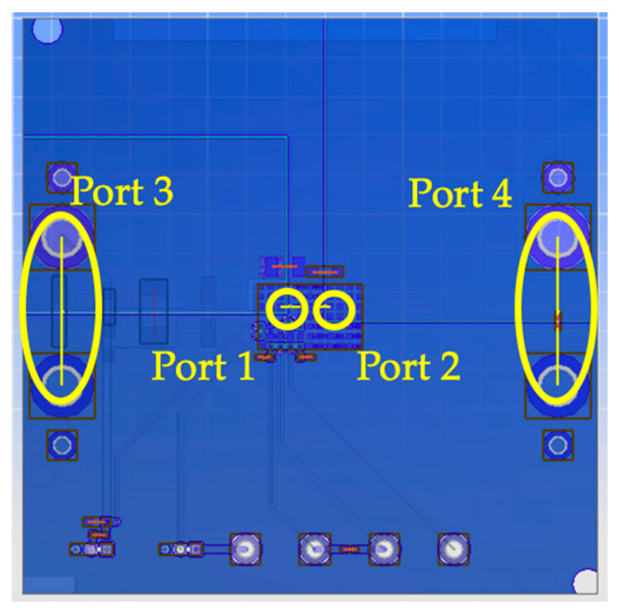
As for the modeling of the in-band characteristics of passive linear components, the extant methods are relatively mature, especially when the parasitic parameters of the main components are known. Therefore, a commercial simulation software Ansys SIwave [31] is used to model the test board DC1379B. ANSYS SIwave is a specialized design platform for modeling, analyzing and simulating of IC packages and PCBs. The test board consisted of four layers; the relative permittivity of the dielectric substrate is ; all conductors are made by copper material with conductivity . The given layout and geometry of the DC1379B were imported into the software. The locations and basic descriptions of the four defined ports are shown in Figure 12 and Table 1.
Therefore, the PCB can be regarded as a four-port network, and the effect of DC1379B on the measured results can be represented by a Y-parameter matrix .
Using the full-wave analysis method, the Y-parameters were calculated. The results are shown in Figure 13.
Theoretically, the output interference signals from the chip pins can be obtained by solving the linear equations of Equation (13) when and are known.
However, since has no phase information, has no phase information either. Therefore, the solution of the complex coefficient Equation (13) may not be unique. Under the test configuration described in this paper, cannot be directly obtained referring the de-embedding process in the ICEM standard.
To solve this problem, the paper proposes a developed vector fitting algorithm as follows.
3.2.2. A Developed Vector Fitting Algorithm
Let and , Equation (2) could be represented as below:
Bring (14) into (10), there is:
or:
Let the auxiliary functions and as
Since and were fitted in the same the process, researchers took as an example to illustrate the algorithm. The traditional vector fitting [32] algorithm makes a clever use of matrix transformation to provide a feasible numerical solution method for solving frequency domain responses rational approximation problems. Contrast with vector fitting algorithm, considering the rational function approximations of the impedance parameter as:
let auxiliary function as
Multiplying the second row in (20) with yields the following relation
However, since were measured by the spectrum analyzer, it contains no phase information. Therefore, it is unable to obtain with accurate phase information. This can greatly affect the accuracy of vector fitting and even lead to serious errors. Therefore, the paper proposed a developed algorithm to reduce the impact of the uncertain phase information. When only the amplitude information is considered, the Equation (20) turns into:
where , , , are unknowns.
It can be seen that Equation (21) is no longer a linear problem. Therefore, the linear least squares optimization process in the original method is changed to a nonlinear problem, and a margin control parameter is added into the iterative process to reduce the impact of the uncertain phase information.
From Equation (21), record the residual function as:
Therefore, the fitting problem on the sample data set can be described by a nonlinear least squares problem as Equation (23).
This nonlinear problem can be solved by the Levenberg-Marquardt algorithm. The pseudo-code algorithm is shown in the reference [33].
Therefore, and could be calculated. According to Equation (17), the values of and can be obtained, and can be obtained from (10) and (11).
As an example, Figure 14 shows the comparison results between the calculated and the predicted which is under the condition that . is represented by the black line in the figure which is as same as the red star in the Figure 3a. Since it was directly converted from the test result , the values of were used as a reference to measure the accuracy of the fitting algorithm. The blue line in the figure shows the predicted result calculated by the traditional vector fitting algorithm, while the red line is estimated by the developed algorithm proposed in this paper. Comparing the two curves, it can be seen that the proposed algorithm can effectively solve the problem that the traditional vector fitting algorithm has low fitting precision when there is no phase information in the fitted data.
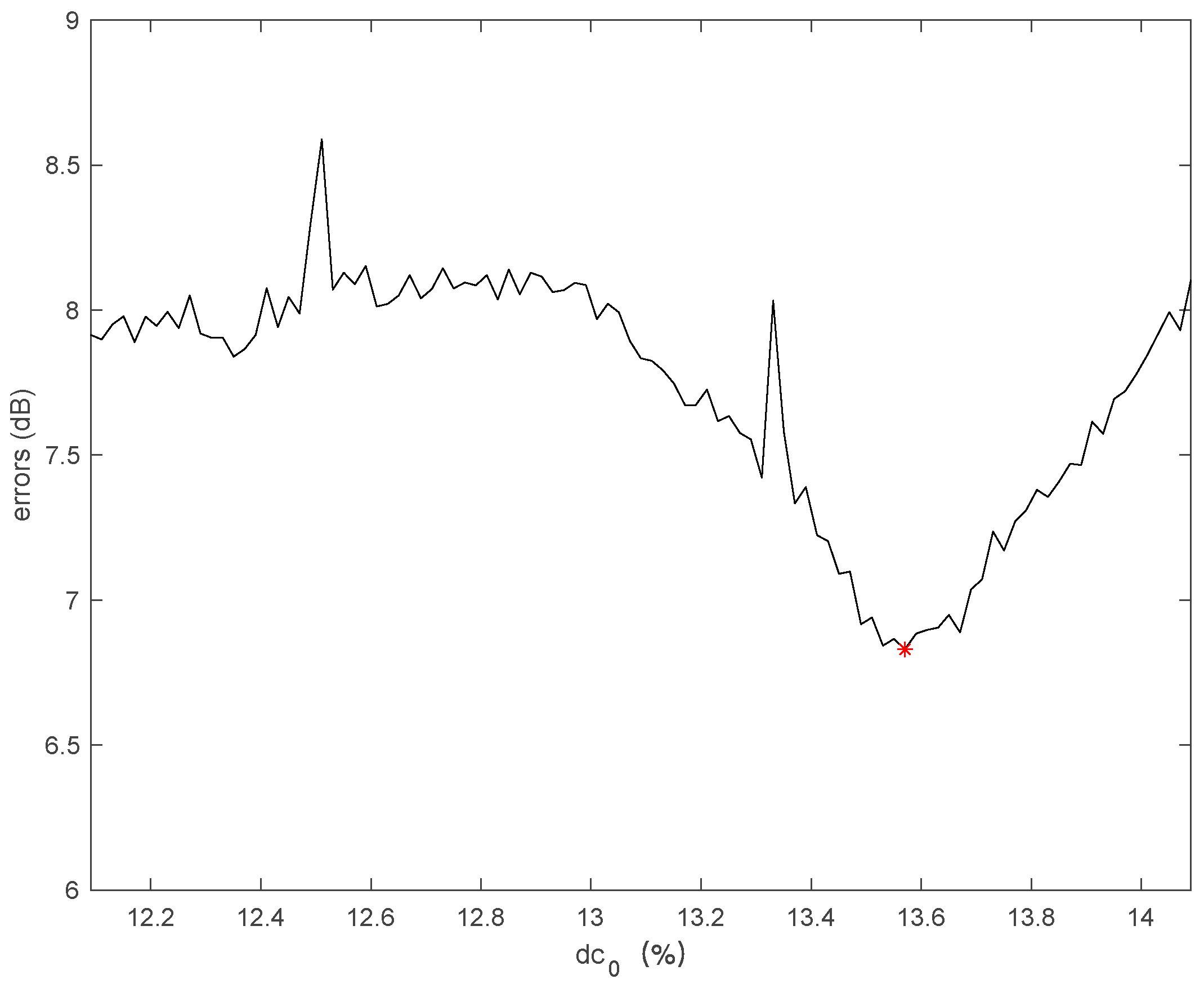
3.2.3. Further Estimation of dc0 and ICPND
Due to the influence of measurement accuracy, etc., the accuracy of the estimated in Section 3.1.2 is limited. Therefore, this subsection describes a process establishing the model of while estimating a more accurate value of .
It can be seen from Equations (10) and (14), is related to the value of . Therefore, the problem can be converted into finding an optimal which minimizes the error between the predicted output and the calculated data , as is shown in (24).
To solve the above mentioned optimization problem (24), errors function was built as the 2-norm of the difference between and at the sample set , which can be represented as:
At this point, (24) can be transformed to minimize (25).
Repeat the above process under different values in the neighborhood of . Then the final duty cycle is estimated as the one which made (25) achieve its minimum. And let the corresponding be the impedance parameters of ICPDN part .
Figure 15 shows the variation of under different , and the red star represents the final estimated result .
4. Experimental Results and Discussion
In this section, an application example and a set of comparative experiments are given to verify the effectiveness of the modeling method.
4.1. Application Example
An application example was taken to verify the accuracy of the above-mentioned modeling method. In this example, the 12 V input voltage were convert to 5.4 V, 5.4 V, and 3.8 V output voltages respectively by three LTM8025 chips. The PCB board adopts a four-layer board structure. Its photo and topology diagram are shown in Figure 16 and Figure 17 respectively.
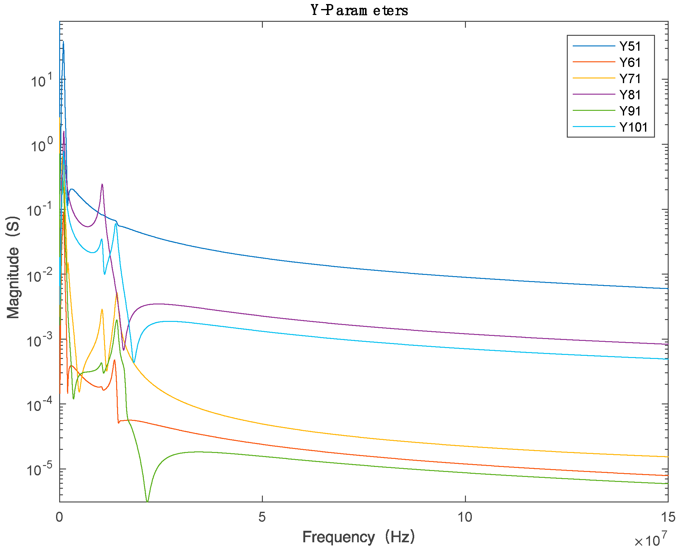
The author treated the PCB sub-module in the instance as a 10-port network and simulated its Y-parameters by Ansys SIwave. The port definitions were shown in Figure 18 and Table 2. And the calculation results were shown in Figure 19.
As for IC sub-modules modeling, according to the design parameters, and of the three chips are as shown in Table 3. Therefore, the functions of the three ICIAs can be calculated according to Equation (10). Furthermore, the CE model of each chip could be obtained according to Equation (6). As an example, the estimated results of IC sub-module 1 are shown in Figure 20.
However, in practical applications, the true value of a resistor often deviates from its nominal value, which may cause the estimated interference spectrum to offset from the measured value. Furthermore, for a regular electromagnetic interference such as switching signals, we tend to pay more attention to the characteristics of its envelope rather than a single frequency point. Therefore, the authors used its envelope to evaluate the accuracy of the estimated result in the following part. At this point, the conducted emission measured result at the port 12Vin could be estimated according to Equation (10).
Figure 21a shows the comparison between the envelope of the measured result (as the red line) and the estimated one (as the blue line). And the forecast errors and its 90% confidence interval are shown in Figure 21b. It can be found that the maximum error is 9.677 dB @23.79 MHz, and its 90% confidence interval is (−4.56 dB, 6.52 dB).
As an authoritative international standard for IC conduction emission modeling, the examples given in the reference [26] suggest that ‘the agreement is very good’ when the forecast error is less than ±10 dB. In contrast, it can be seen that the modeling method proposed in this paper could achieve the standard requirements and has sufficient accuracy and effectiveness.
4.2. Comparative Experiments
According to ICEM of test configurations described in the reference [26], a dedicated chip test board for LTM8025 is made. In order to ensure the normal operation of the tested chip, the resonance resistance and the bias resistance are set. Using the impedance analyzer and the oscilloscope to measure the impedance curve and output waveform of the chip. The ICEM model is obtained, and the following two comparative experiments are used to illustrate the practicality of the algorithm. With reference to DC1379B, the authors created three demo boards with different parameter settings as models to be used for comparison experiments.
Table 4 shows the parameter settings for the three demo boards. It can be seen that the parameter settings of Board 1 are same with the ICEM test board while the other two boards are different.
It should be noted that since the impedance analyzer used in ICEM modelling process only covers a frequency band from 20 kHz to 100 MHz, the CE predicted results were only considered in this range in the comparison experiments.
● Board 1: The usage parameters are same as the ICEM test board.
When the actual board parameter settings are exactly same as the ICEM test board, the two methods are used to predict the conducted emissions separately. The comparison results are shown in Figure 22.
It can be seen that in this case, the 90% confidence intervals of the two methods are (−6.82 dB, 7.32 dB) and (−7.04 dB, 7.54 dB), respectively. The accuracy of the two modeling methods is not much different. Both the proposed method and ICEM method can meet the requirements for CE prediction.
● Board 2 and Board 3: The usage parameters are different with the ICEM test board.
To make it different from the ICEM test board parameter settings, the author changed the main components of the actual board as Board 2 which is shown in Table 4. CE of the actual board at its voltage input port was predicted by the two methods respectively. The comparison results are shown in Figure 23.
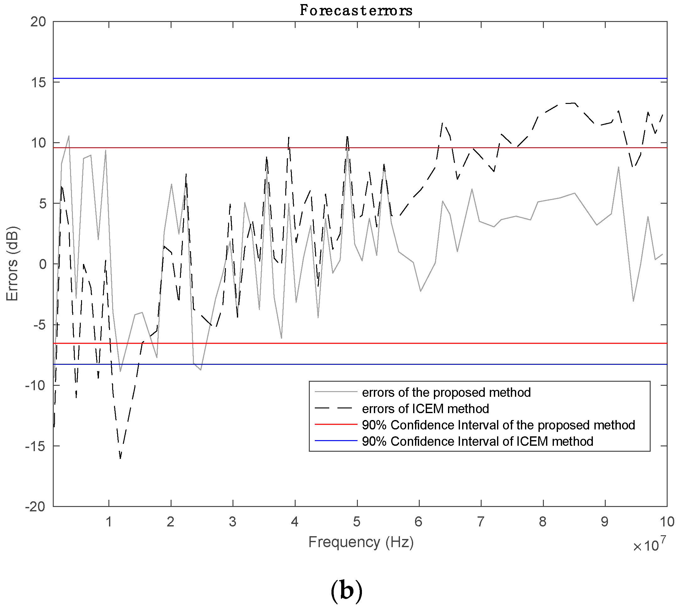
What the comparison results show are as following. Although the accuracy of the ICEM method is similar with the proposed method approximately to the middle of the considered frequency band, it decreases significantly with increasing frequency. As a statistical result, the 90% confidence interval of forecast errors is (−6.54 dB, 9.56 dB) by the proposed method, while (−8.28 dB, 15.29 dB) though the ICEM method.
Another comparative test board parameter setting are as Board 3 shown in Table 4, and the comparison results are shown in Figure 24.
It can be seen from the comparison results that the accuracy of the proposed method is still acceptable after changing the board’s design parameter settings. Except for a minimum point near 8 MHz, the forecast error is less than 10 dB in almost the entire considered frequency band. The 90% confidence interval of forecast errors is (−7.53 dB, 6.46 dB). Unfortunately, the ICEM method does not perform well in the CE prediction of Board 3. The forecast error is much larger than 10 dB in the frequency bands below 10 MHz or above 60 MHz. In particular, when the CE has obvious periodic variation characteristics, the ICEM method can only describe the trend roughly but cannot effectively describe its envelope. The 90% confidence interval of forecast errors is (−8.29 dB, 17.6 dB).
From the above mentioned comparison results we can find that when the parameters of the actual circuit are different from the test board, the modeling accuracy of ICEM modeling method is greatly reduced. This is because the interference signal generated by the SMPS chip is related to the parameter setting of the external circuit. In the ICEM method, the IA modeling is reliant entirely on the measured results and without considering its association with peripheral parameters. Therefore, when the actual circuit used is inconsistent with the test board parameters, the ICEM model will no longer be applicable. In practical applications, since the circuit parameters have not been determined during the product design stage, a huge number of test boards with different parameter settings are needed when we use the ICEM method to predict the conduction emission. The workload it brings are enormous.
Otherwise, the method proposed in this paper fully considers the mechanism of interference generation. It found the relationship between emission characteristics and peripheral circuit parameters, and established a parametric CE model of the SMPS chip. Therefore, it is more convenient in actual use, since only the model parameters need to be adjusted as required without further measuring.
In summary, compared with the traditional ICEM modeling method, the proposed modeling method has better applicability in the product design stage under the premise of ensuring that the modeling accuracy is not reduced.
5. Conclusions
This paper proposes a modeling method to establish a parametric-conducted emission model of a switching model power supply (SMPS) chip through a developed vector-fitting algorithm. Reference the ICEM standard, the parametric conducted emission model is also divided into two parts: ICIA and ICPDN. The parameters of ICIA are identified by measured data and correlated with key components; an improved vector fitting algorithm is proposed to solve the fitting problem of ICPDN without phase information. The experimental results show that the proposed method could achieve the international standard requirements and has sufficient accuracy and effectiveness.
Author Contributions
X.H. proposed, designed and wrote the paper; S.X. supervised the experiments and write-up of the paper; Z.C. helped in carrying out experiments.
Funding
This research was funded by National Natural Science Foundation of China (No.61271045) and Defense Industrial Technology Development Program (No.JCKY2016601B005).
Conflicts of Interest
The authors declare no conflict of interest.
References
- Ding, F.; Zhang, J. Analysis and design for VMS EMC based on MPC555. World Electr. Veh. J. 2010, 4, 754–759. [Google Scholar] [CrossRef]
- Krug, F.; Lewke, B. Electromagnetic interference on large wind turbines. Energies 2009, 2, 1118–1129. [Google Scholar] [CrossRef]
- Podbersic, M.; Matko, V.; Segula, M. An EMI filter selection method based on spectrum of digital periodic signal. Sensors 2006, 6, 90–99. [Google Scholar] [CrossRef]
- Gulez, K.; Mutoh, N. Application of Neural Networks to Estimate Common Mode (CM) Model Impedance Parameters in AC Drives. Math. Comput. Appl. 2003, 8, 225–233. [Google Scholar] [CrossRef] [Green Version]
- Ran, L.; Gokani, S.; Clare, J.; Bradley, K.J.; Christopoulos, C. Conducted electromagnetic emissions in induction motor drive systems. I. time domain analysis and identification of dominant modes. IEEE Trans. Power Electron. 1998, 13, 757–767. [Google Scholar] [CrossRef]
- Rondon-Pinilla, E.; Morel, F.; Vollaire, C.; Schanen, J.L. Modeling of a Buck Converter with a SiC JFET to Predict EMC Conducted Emissions. IEEE Trans. Power Electron. 2014, 29, 2246–2260. [Google Scholar] [CrossRef]
- Zhai, L.; Cao, Y.; Lin, L.; Zhang, T.; Kavuma, S. Mitigation Conducted Emission Strategy Based on Transfer Function from a DC-Fed Wireless Charging System for Electric Vehicles. Energies 2018, 11, 477. [Google Scholar] [CrossRef]
- Zhai, L.; Zhang, X.; Bondarenko, N.; Loken, D.; Van Doren, T.; Beetner, D. Mitigation emission strategy based on resonances from a power inverter system in electric vehicles. Energies 2016, 9, 419. [Google Scholar] [CrossRef]
- Bishnoi, H.; Baisden, A.C.; Mattavelli, P.; Boroyevich, D. Analysis of EMI Terminal Modeling of Switched Power Converters. IEEE Trans. Power Electron. 2012, 27, 3924–3933. [Google Scholar] [CrossRef]
- Frantz, G.; Frey, D.; Schanen, J.L.; Revol, B. EMC models of Power Electronics converters for network analysis. In Proceedings of the European Conference on Power Electronics & Applications, Lille, France, 2–6 September 2013. [Google Scholar]
- Labrousse, D.; Revol, B.; Gautier, C.; Costa, F. Fast Reconstitution Method (FRM) to Compute the Broadband Spectrum of Common Mode Conducted Disturbances. IEEE Trans. Electromagn. Compat. 2013, 55, 248–256. [Google Scholar] [CrossRef]
- Ghfiri, C.; Durier, A.; Boyer, A.; Dhia, S.B.; Marot, C. Construction of an Integrated Circuit Emission Model of a FPGA. In Proceedings of the Asia-Pacific International Symposium on Electromagnetic Compatibility, Shenzhen, China, 17–21 May 2016; pp. 402–405. [Google Scholar]
- Ramanujan, A.; Sicard, E.; Boyer, A.; Levant, J.L.; Marot, C.; Lafon, F. Developing a Universal Exchange Format for Integrated Circuit Emission Model—Conducted Emissions. In Proceedings of the 2015 10th International Workshop on the Electromagnetic Compatibility of Integrated Circuits (EMC Compo), Edinburgh, UK, 10–13 November 2015. [Google Scholar]
- Funabiki, N.; Nomura, Y.; Kawashima, J.; Minamisawa, Y.; Wada, O. A LECCS model parameter optimization algorithm for EMC designs of IC/LSI systems. In Proceedings of the 2006 17th International Zurich Symposium on Electromagnetic Compatibility 2006, Singapore, 28 February–3 March 2006. [Google Scholar]
- Ramdani, M.; Sicard, E.; Boyer, A.; Dhia, S.B.; Whalen, J.J.; Hubing, T.H.; Coenen, M.; Wada, O. The Electromagnetic Compatibility of Integrated Circuits—Past, Present, and Future. IEEE Trans. Electromagn. Compat. 2009, 51, 78–100. [Google Scholar] [CrossRef]
- I/O Buffer Information Specification (IBIS). 2008. Available online: http://www.eigroup.org/ibis/ibis.htm (accessed on 5 May 2019).
- IEC 62404. International Electro-Technical Commission: I/O Interface Model for Integrated Circuit (IMIC). IEC Standard, 2003. Available online: www.iec.ch (accessed on 5 May 2019).
- IEC 62014-3. International Electro-Technical Commission: Models of Integrated Circuits. IEC Standard, 2002. Available online: www.iec.ch (accessed on 5 May 2019).
- Lochot, C.; Levant, J. ICEM: A new standard for EMC of IC definition and examples. In Proceedings of the 2003 IEEE Symposium on Electromagnetic Compatibility, Boston, MA, USA, 18–22 August 2003. [Google Scholar]
- Ghfiri, C.; Boyer, A.; Durier, A.; Dhia, S.B. A new methodology to build the Internal Activity Block of ICEM-CE for complex Integrated Circuits. IEEE Trans. Electromagn. Compat. 2018, 60, 1500–1509. [Google Scholar] [CrossRef]
- Capriglione, D.; Chiariello, A.; Maffucci, A. Accurate Models for Evaluating the Direct Conducted and Radiated Emissions from Integrated Circuits. Appl. Sci. 2018, 8, 477. [Google Scholar] [CrossRef]
- Levant, J.L.; Ramdani, M.; Perdriau, R.; Drissi, M.H. EMC Assessment at Chip and PCB Level: Use of the ICEM Model for Jitter Analysis in an Integrated PLL. IEEE Trans. Electromagn. Compat. 2007, 49, 182–191. [Google Scholar] [CrossRef]
- Park, H.H.; Song, S.H.; Han, S.T.; Jang, T.S.; Jung, J.H.; Park, H.B. Estimation of Power Switching Current by Chip-Package-PCB Cosimulation. IEEE Trans. Electromagn. Compat. 2010, 52, 311–319. [Google Scholar] [CrossRef]
- Labussière-Dorgan, C.; Bendhia, S.; Sicard, E.; Tao, J.; Quaresma, H.J.; Lochot, C.; Vrignon, B. Modeling the Electromagnetic Emission of a Microcontroller Using a Single Model. IEEE Trans. Electromagn. Compat. 2008, 50, 22–34. [Google Scholar] [CrossRef]
- Li, S.; Bishnoi, H.; Whiles, J.; Ng, P.; Weng, H.; Pommerenke, D.; Beetner, D. Development and validation of a microcontroller model for EMC. In Proceedings of the 2008 International Symposium on Electromagnetic Compatibility—EMC Europe, Amsterdam, The Netherlands, 27–30 August 2008. [Google Scholar]
- IEC 62433-2. International Electro-Technical Commission: EMC IC modelling: Models of Integrated Circuits for EMI Behavioral Simulation—Conducted Emissions Modelling (ICEM-CE). IEC Standard, 2008. Available online: www.iec.ch (accessed on 5 May 2019).
- Su, D.; Xie, S.; Chen, A.; Shang, X.; Zhu, K.; Xu, H. Basic Emission Waveform Theory: A Novel Interpretation and Source Identification Method for Electromagnetic Emission of Complex Systems. IEEE Trans. Electromagn. Compat. 2018, 60, 1330–1339. [Google Scholar] [CrossRef]
- LTM8025 Datasheet and Product Info. Available online: https://www.analog.com/en/products/ltm8025.html (accessed on 5 May 2019).
- DC1379B Product Details. Available online: https://www.analog.com/en/design-center/evaluation-hardware-and-software/evaluation-boards-kits/dc1379b.html (accessed on 5 May 2019).
- F-33-2 Datasheet. Available online: http://www.fischercc.com/products/f-33-2/ (accessed on 20 May 2019).
- Ansys SIwave. Available online: https://www.ansys.com/products/electronics/ansys-siwave (accessed on 25 March 2019).
- Gustavsen, B.; Semlyen, A. Rational approximation of frequency domain responses by vector fitting. IEEE Trans. Power Deliv. 2002, 14, 1052–1061. [Google Scholar] [CrossRef]
- Moré, J.J. The Levenberg-Marquardt algorithm: Implementation and theory. Lect. Notes Math. 1978, 630, 105–116. [Google Scholar]
Figure 1.
Board diagram and schematic of DC1379B [29]. (a) Printed circuit board (PCB) and its layouts; (b) Schematic.
Figure 1.
Board diagram and schematic of DC1379B [29]. (a) Printed circuit board (PCB) and its layouts; (b) Schematic.


Figure 2.
Experimental scenario of the test board at (a) VIN port; (b) VOUT port conduction emissions.
Figure 2.
Experimental scenario of the test board at (a) VIN port; (b) VOUT port conduction emissions.

Figure 3.
The measured results (a) the measured conducted emission at the port VIN; (b) the measured conducted emission at the port VOUT.
Figure 3.
The measured results (a) the measured conducted emission at the port VIN; (b) the measured conducted emission at the port VOUT.


Figure 4.
IC conducted emission model partitioning. ICIA and ICPDN.

Figure 5.
Frequency interval changes in one test.

Figure 6.
Δfi selecting process.

Figure 7.
The curve of repetition frequency f0 under different values of resonance resistance RT.

Figure 8.
The curve of duty cycle dc0 under different value of Vout/Vin.

Figure 9.
De-embedding principle [26].
Figure 9.
De-embedding principle [26].

Figure 10.
The block diagram of the measurement setup.

Figure 11.
The calibration curve of F-33-2 [30].
Figure 11.
The calibration curve of F-33-2 [30].

Figure 12.
Port definitions of DC1379B.

Figure 13.
Y parameter simulation results.

Figure 14.
The predicted results at the port VIN.

Figure 15.
The errors curve under different dc0.

Figure 16.
Photos of the power supply module instance. (a) PCB and its layouts; (b) Experimental scenario.
Figure 16.
Photos of the power supply module instance. (a) PCB and its layouts; (b) Experimental scenario.

Figure 17.
The topology of the power supply module.

Figure 18.
Port definitions of the power supply module instance.

Figure 19.
Y parameter simulation results between the Port 1 and other internal ports.

Figure 20.
The estimated results of the IC sub-module 1.

Figure 21.
Comparison between the measured result and the estimated one. (a) Predicted results; (b) forecast errors.
Figure 21.
Comparison between the measured result and the estimated one. (a) Predicted results; (b) forecast errors.

Figure 22.
Comparison between the proposed method and ICEM method for Board 1. (a) Predicted results; (b) forecast errors.
Figure 22.
Comparison between the proposed method and ICEM method for Board 1. (a) Predicted results; (b) forecast errors.


Figure 23.
Comparison between the proposed method and ICEM method for Board 2. (a) Predicted results; (b) forecast errors.
Figure 23.
Comparison between the proposed method and ICEM method for Board 2. (a) Predicted results; (b) forecast errors.


Figure 24.
Comparison between the proposed method and ICEM method for Board 4. (a) Predicted results; (b) forecast errors.
Figure 24.
Comparison between the proposed method and ICEM method for Board 4. (a) Predicted results; (b) forecast errors.


Table 1.
Parameter settings of each port.
| No. | Name | Description |
|---|---|---|
| 1 | IC_in | Internal port: IC input voltage port |
| 2 | IC_out | Internal port: IC output voltage port |
| 3 | VIN | External port: PCB input voltage port |
| 4 | VOUT | External port: PCB output voltage port |
Table 2.
Parameter settings of each port.
| No. | Name | Description |
|---|---|---|
| 1 | 12Vin | External port: PCB input voltage port |
| 2 | 5.4Vout_1 | External port: PCB output voltage port (comes from IC3) |
| 3 | 5.4Vout_2 | External port: PCB output voltage port (comes from IC 2) |
| 4 | 3.8Vout | External port: PCB output voltage port (comes from IC 1) |
| 5 | IC1_in | Internal port: IC1 input voltage port |
| 6 | IC1_out | Internal port: IC1 output voltage port |
| 7 | IC2_in | Internal port: IC2 input voltage port |
| 8 | IC2_out | Internal port: IC2 output voltage port |
| 9 | IC3_in | Internal port: IC3 input voltage port |
| 10 | IC3_out | Internal port: IC3 output voltage port |
Table 3.
Design parameters of the three chips.
| RT (kΩ) | f0 (kHz) | Vin (V) | Vout (V) | dc0 (%) | |
|---|---|---|---|---|---|
| IC 1 | 39.5 | 890.7 | 12 | 5.4 | 38.83 |
| IC 2 | 22 | 1377.5 | 12 | 5.4 | 54.96 |
| IC 3 | 20 | 1468.9 | 12 | 3.8 | 54.96 |
Table 4.
Design parameters of the three boards.
| (kΩ) | (kHz) | (kΩ) | (V) | (V) | (%) | |
|---|---|---|---|---|---|---|
| Board 1 | 15 | 1745.4 | 200 | 5.8 | 2.75 | 57.88 |
| Board 2 | 27 | 1180.5 | 75 | 10 | 5.87 | 71.52 |
| Board 3 | 42 | 847.6 | 115 | 5.8 | 4.21 | 88.36 |
© 2019 by the authors. Licensee MDPI, Basel, Switzerland. This article is an open access article distributed under the terms and conditions of the Creative Commons Attribution (CC BY) license (http://creativecommons.org/licenses/by/4.0/).
Share and Cite
MDPI and ACS Style
Hao, X.; Xie, S.; Chen, Z. A Parametric Conducted Emission Modeling Method of a Switching Model Power Supply (SMPS) Chip by a Developed Vector Fitting Algorithm. Electronics 2019, 8, 725. https://doi.org/10.3390/electronics8070725
AMA Style
Hao X, Xie S, Chen Z. A Parametric Conducted Emission Modeling Method of a Switching Model Power Supply (SMPS) Chip by a Developed Vector Fitting Algorithm. Electronics. 2019; 8(7):725. https://doi.org/10.3390/electronics8070725
Chicago/Turabian StyleHao, Xuchun, Shuguo Xie, and Ziyao Chen. 2019. "A Parametric Conducted Emission Modeling Method of a Switching Model Power Supply (SMPS) Chip by a Developed Vector Fitting Algorithm" Electronics 8, no. 7: 725. https://doi.org/10.3390/electronics8070725
Note that from the first issue of 2016, this journal uses article numbers instead of page numbers. See further details here.