Article

Modulation Strategy with a Minimal Number of Commutations for a Five-Level H-Bridge NPC Inverter

1
Naval Academy Research Institute, Ecole Navale CC-600, F-29240 Brest CEDEX 9, France
2
ECAM Strasbourg Europe—ICube laboratory (UMR7357), F-67400 Illkirch-Graffenstaden, France
3
Institut Jean Lamour (UMR7198), Université de Lorraine, 54000 Nancy, France
4
GREEN Laboratory, Université de Lorraine, 54000 Nancy, France
*
Author to whom correspondence should be addressed.
Electronics 2019, 8(4), 454; https://doi.org/10.3390/electronics8040454
Submission received: 13 February 2019 / Revised: 17 April 2019 / Accepted: 18 April 2019 / Published: 23 April 2019
(This article belongs to the Special Issue Power Converters in Power Electronics)

Abstract

:
In this paper, a so-called OPTimized Pulse Width Modulation (OPT-PWM) strategy with a minimal number of commutations for a multilevel converter (MC) is proposed. The principle is based on the reduction of the number of switch commutations by removing the unnecessary ones for each voltage level transition. The OPT-PWM strategy is applied to a five-level H-Bridge Neutral Point Clamped (HB-5L-NPC) inverter. A specific block based on a state machine is added to conventional modulation techniques to perform the transitions from a given voltage level to another one via the best trajectory with a minimal number of commutations. The principle of this additional block can be applied to any modulation technique. In this paper, the proposed strategy is validated first by simulation and then through experimental tests.

1. Introduction

In recent decades, the use of power converters in high-power and medium-voltage (MV) industrial applications such as the integration of renewable resources, distributed power generation systems, microgrids, energy storage systems, and motor drives has significantly increased. There are two major families for voltage source inverters (VSI): two-level and multilevel inverters (MLI) where the prefix “multi” means any integer greater than two. In MV applications, with respect to device rating limits, MLI has attracted increasing attention in the last decade. MLI provides significant advantages for these applications. Among these advantages, the THD (Total Harmonic Distortion) improvement in output signals at low switching frequencies is most discussed in the literature. Due to this improvement, the size of the output passive filters can be reduced. Moreover, a lower switching frequency allows performance with higher efficiency [1].
In the literature, four major multilevel inverters are commonly studied [2]: Neutral Point Clamped (NPC) [3,4,5,6,7,8,9,10], Flying Capacitor (FC) [11,12], Cascaded H-Bridge (CHB) [13,14], and Modular Multilevel Converter (MMC) [15,16]. They have major advantages compared to two-level inverters, mainly because they operate at lower switching frequencies. More, they provide a higher number of levels; thus, the staircase waveform is increased. In a recent review paper [17], these attractive features of MLI are highlighted and discussed.
In addition, modulation techniques are very often discussed in the literature [1,8,15]; they aim to perform harmonic reduction of the system for the same converter output power but at lower switching frequency [1,17]. The originality of this paper is to propose an additional advanced functionality for the modulation strategy that evaluates possible switching trajectories in multilevel inverters and implements the trajectory with a minimal number of commutations. The proposed advanced functionality can also be applied to any modulation strategy and provides a significant improvement compared with modulation approaches published in the literature.
In this paper, a five-level H-bridge NPC (HB-5L-NPC) inverter controlled by an OPTimized Pulse Width Modulation (OPT-PWM) strategy is proposed. The goal of the proposed OPT-PWM control is to perform the minimal number of commutations when the conventional Level Shift-PWM (LS-PWM) control is used. This means that this control method produces the same output voltage as the conventional LS-PWM but with a reduced number of switch commutations.
Applying the proposed OPT-PWM on MMCs can be useful to reduce switching losses and consequently improve the efficiency and the lifetime of the converters. In multilevel converters, even at low frequencies, the switching power losses of the applied IGBT (Insulated Gate Bipolar Transistor) devices are considerable. As an example, they can amount to roughly one-third of the total losses if 4.5 kV IGBT components are used [18]. Thus, there is a permanent requirement for further improvement of efficiency by power loss reduction, especially in the high-power range applications where energy cost and cooling equipment are mainly concerned [18]. A few works have studied some modulation strategies to minimize the number of commutation processes in matrix converters [19,20]. In reference [21], an advanced model predictive control technique was proposed for a back-to-back NPC converter; this control was applied to wind energy conversion systems (WECS). By applying the proposed predictive control, the authors considered the redundant switching states of a converter to reduce the number of commutations. The presented results show that the active power delivered to the grid was increased where the extracted power of the generator was constant [21]. This means that the reduction in the number of commutations decreases the power loss in the converter. In the same spirit, this paper presents a so-called OPT-PWM modulation strategy that removes unnecessary switching to reduce the number of commutations per switching cycles with respect to the classical modulation strategy.
According to surveys [22,23], one of the semiconductor aging processes is the accumulation of electrical switching cycles (ΔV and Δi cycles) that cause metallurgical defects on the semiconductor die and change the electrical characteristics as well [23]. Therefore, a reduction in the number of commutations can also postpone the aging of the semiconductor.
The paper is organized as follows. The next section presents the proposed HB-5L-NPC converter and all the possible output voltage levels. The proposed OPT-PWM control is detailed in Section 3. Simulation results for the HB-5L-NPC inverter are presented in Section 4, and experimental tests are presented and discussed in Section 6, followed by a general conclusion in the last section.

2. Studied System Description

The system studied in this paper is shown in Figure 1; it is based on a single-phase HB-5L-NPC. The converter supplies an inductive load (R, L series). The proposed HB-5L-NPC consists of two parallel connected 3-level NPC (Figure 2a). Each 3-level NPC consists of four switches and six diodes (Figure 2b). The DC bus consists of two identical capacitors C, connected in series, where the midpoint is denoted ‘O’.

2.1. Control of the HB-5L-NPC by Classical LS-PWM

To control the converter, a conventional modulation strategy was considered. The block LS-PWM in Figure 1 generates the switching patterns by comparing two triangular carriers with two sinusoidal references. As shown in Figure 3a, the positive triangular carrier signal (Car_Pos) and the sinusoidal reference (Ref_Pos) are used to generate the control signals for the switches T11 and T13 (leg1 for 3-level HB-NPC in Figure 3b). To generate the control signals of the components T12 and T14 (Leg1), the positive sinusoidal reference is compared with the negative triangular signal (Car_Neg). The controls for the four switches of the Leg2 (T21, T22, T23, and T24) are generated by comparing the negative sinusoidal reference (Ref_Neg) with the two carriers. The generated outputs of the LS-PWM block and the control signals are given in Figure 3b. Thus, as can be seen, the output voltage (at the bottom of Figure 3b) behavior has five levels (−Vdc, −Vdc/2, 0, Vdc/2, and Vdc).

2.2. Simulation Results for the HB-5L-NPC Converter Controlled by LS-PWM

Some simulations in the Matlab/Simulink environment using the SimPowerSystem library were performed to study the system depicted in Figure 2. The simulation results illustrate the possibility of reducing the number of commutations. The system parameters are introduced in Table 1, where fpwm is the PWM switching frequency and m is the modulation index.
The simulation results for the output voltage are shown in Figure 4. As mentioned before, the goal of this paper is to propose an additional advanced functionality for the modulation strategy that provides the minimal number of switch commutations. For this, let us first analyze the output voltage generated by the classical LS-PWM, as given in Figure 4.

2.3. The Switching Number Reduction

As indicated in Figure 4, some small variations in the output voltage Vo(t) at the Vdc/2 and −Vdc/2 levels occur. To better understand our approach, these small variations are highlighted in Zooms 1 to 4 in Figure 4.
These small variations are not generated by changes in the level of the output voltage and are due to some switch commutations. It is clear that when the output voltage reference level remains the same (equal to Vdc/2 or −Vdc/2), it is not necessary to have any commutations. In order to clarify the origin of these voltage variations, the 18 possible combinations (states) of the eight switches to generate a given output voltage level (Vo) are illustrated in Figure 5. In this figure, a state SX (with x from 1 to 18) corresponds to the realization of a given voltage level obtained by on-state switches of the converter (in red color).
In Figure 5, when the requested output voltage level is equal to Vdc/2 (in the case where i(t) > 0), there are two possibilities (states S2 and S3). Therefore, only T11 and T24 can be commuted when the states change (but Vo remains the same). When the requested voltage level is equal to −Vdc/2 (with i(t) < 0, states S16 and S17) only T14 and T21 are switching. Thus, only the corresponding switching patterns are analyzed.
In order to understand what happens during these four intervals (Zooms 1 to 4), the simulation results of the output voltage were observed. To confirm the commutation of one switch, not only were the switching patterns (sent by the LS-PWM block to the switch) observed but the currents passing in the switches were also verified. Figure 6, Figure 7, Figure 8 and Figure 9 give the switching patterns and the associated switch currents during the highlighted phases in Figure 4 (Zooms 1 to 4).
As illustrated in Figure 6, Figure 7, Figure 8 and Figure 9, the output voltage Vo(t) is not constant and small variations occur while it should be constant and equal to Vdc/2. The currents and switching patterns confirm that these oscillations are due to unnecessary commutations. For example, in Figure 6, the converter is in state S2 and then passed to state S3 (Figure 5). Both states generate Vo = Vdc/2; therefore, four unnecessary commutations for the same output voltage level are generated. These commutations inevitably decrease the efficiency of the converter. Therefore, to improve the efficiency of the converter, these unnecessary commutations should be avoided. After analyzing all switching patterns and currents over one period of Vo, it is confirmed that the unnecessary commutations occur only in the considered four zones (detailed before). In the next section, the proposed advanced modulation strategy to eliminate some 16 unnecessary commutations per period is developed.

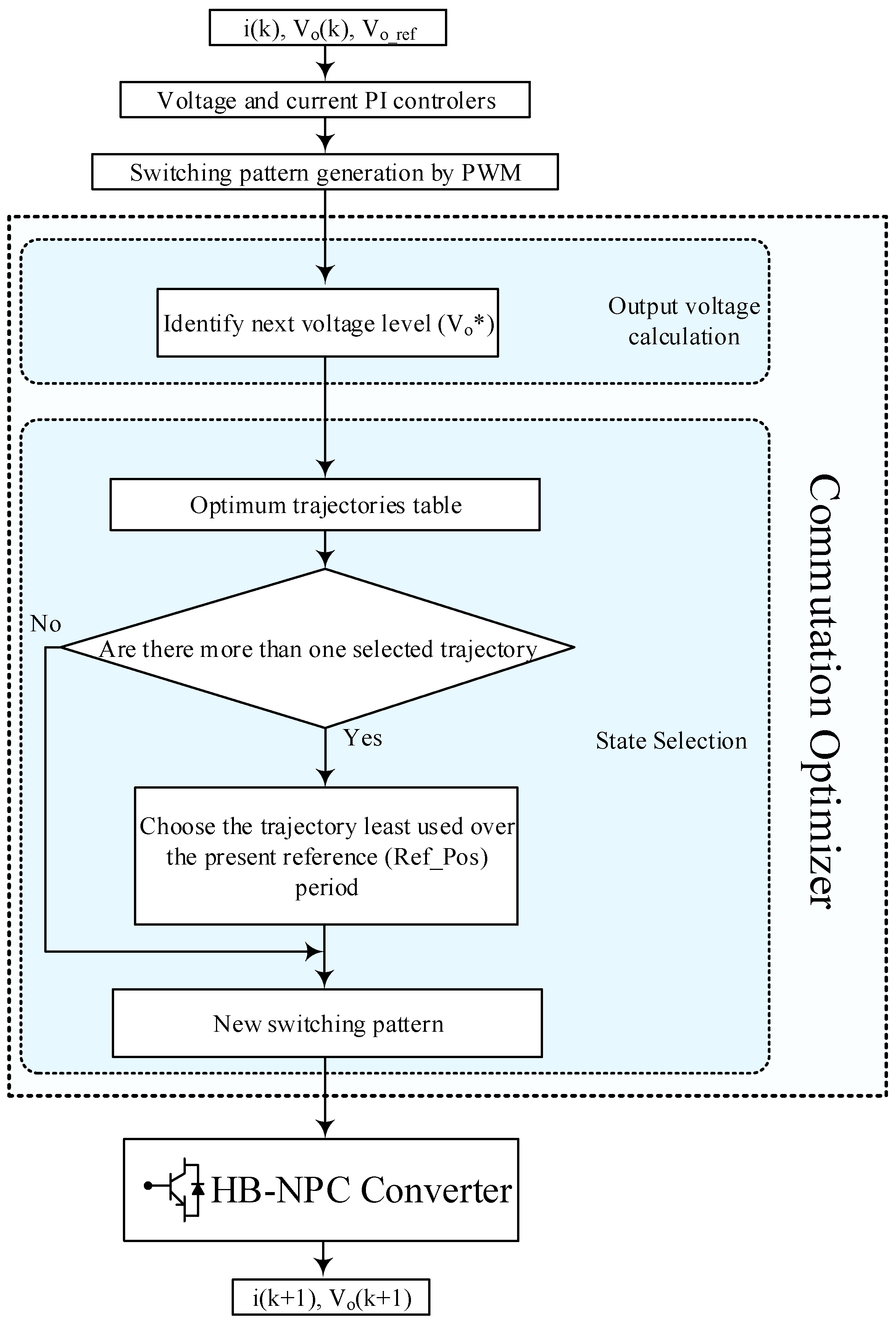
3. The Principle of the Proposed OPT-PWM Strategy

As mentioned before, several modulation strategies have been conventionally proposed in the literature to control the output voltage of multilevel inverters [17]. In this paper, to illustrate our contribution, the classical LS-PWM is considered and an additional block is proposed to provide a minimal number of commutations. Nevertheless, any conventional PWM method can be used ([1,8,15] and [24,25,26,27]), and the same modification of the modulation strategy we propose can be applied in all cases.
Before discussing the OPT-PWM, it is necessary to define the following terms used in this paper:
  • Transition: passing from one state to another one.
  • Trajectory: A trajectory is made up of all the transitions that make it possible to pass from the initial output voltage level to the desired voltage level. A trajectory may consist of one or more transitions.
  • NOT: number of transitions for a trajectory.
  • NOC: number of commutations.
  • NOCSx-Sy: number of commutations to switch from state Sx to state SY.
  • NOCtotal: total number of commutations made by the switches during a trajectory.
Figure 10 illustrates the principle of the OPT-PWM proposed in this paper. This method selects a trajectory with a minimal number of commutations after analyzing all possible trajectories to pass from the initial voltage level to the desired voltage level.
In the first step, the requested voltage level (Vo*) will be determined by using the switching patterns generated by the conventional PWM block used in the classical modulation strategy. Then, the state selection algorithm will find the best trajectory and states to obtain the voltage level Vo* with a minimal number of commutations. This is performed by the “Commutation Optimizer” block given in Figure 10. This optimization only depends on the initial and final voltage levels and consequently does not depend on the used modulation strategy.

3.1. Determination of the Voltage Level Vo*

For the commutation optimizer algorithm to find the best trajectory, the reference voltage level (Vo*) has to be determined. Based on the 18 possible states (Figure 5), suitable control was predefined and is recorded in Table 2. As an example for the state S1, the switches T11, T12, T22, and T24 should be “on” whereas the other switches are “off”. Then, the block called “Output Voltage Calculation” compares the generated PWM switching patterns with the predefined table (Table 2) to find the required voltage level Vo*.

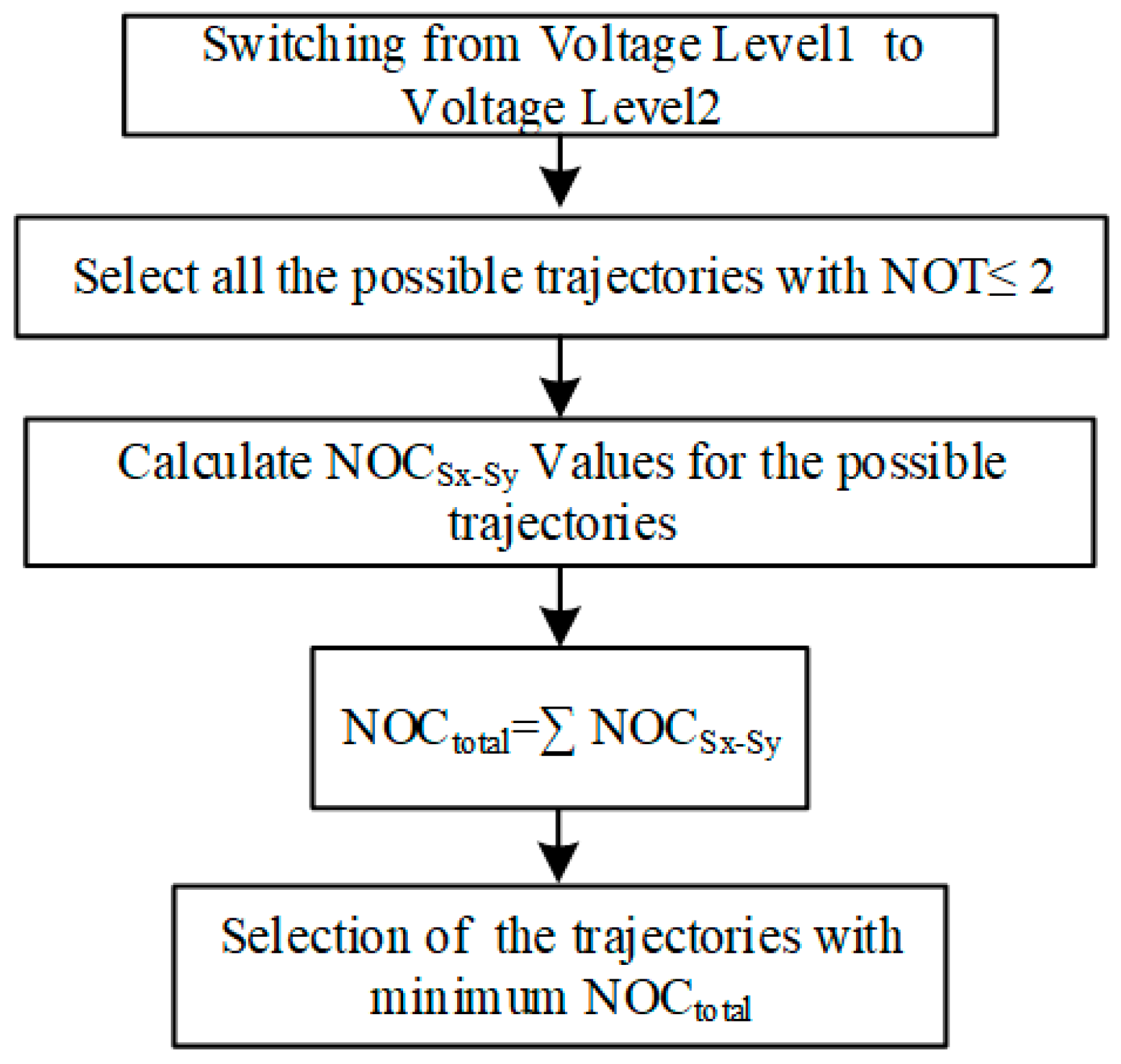
3.2. Search for the Trajectory with a Minimal Number of Commutations

Once the output voltage Vo* (Figure 10) is fixed by the classical PWM control, a second block called “State Selection” selects the best state and trajectory with the minimum number of commutations to perform the required voltage level.
To pass from one level of voltage to another, several trajectories are possible. In addition, each trajectory can contain several transitions between different states. Each transition (SX → SY) is associated with a given number of commutations (NOCSx-Sy), directly related to the number of switches changing their status (on ↔ off) from SX to SY (one voltage level to another). Thus, to achieve the goal of this method, the total number of commutations (NOCtotal) during each change in the output voltage level has to be minimized. For this, all possible trajectories are observed. It is clear that NOC increases with the number of transitions (NOT). To accelerate the execution of the proposed algorithm, the trajectories with more than two transitions are ignored. Indeed, in all cases, the maximum value of NOT will be equal to 2, which allows selecting the optimal trajectories. After trajectory selection, the NOC of each transition and then NOCtotal is calculated. Finally, the trajectory with the minimum NOCtotal is selected.
The optimal trajectory search method is summarized in the flowchart presented in Figure 11. This algorithm is used to determine the optimal trajectory for one change in voltage level. Note that this algorithm (Figure 11) can lead to the choice of one or more trajectories. In the case where more than one trajectory is chosen, the trajectory using the switches which had the lowest number of commutations during the period before will be selected.

3.3. Selection of an Optimized Trajectory out of the Optimal Trajectories

As mentioned before, the “Output Voltage Calculation” block (Figure 10) compares the switching patterns generated by the PWM (δij) to the possible states in Table 2 to find the corresponding state. Once the concerned state is obtained, the value of the next output voltage level (Vo*) is known. As illustrated in Figure 5, each voltage level may have more than one state. Now, the task of the “State Selection” block is the selection of a trajectory with the minimal NOCtotal to pass from SX (actual state) to Sy (the state with Vo*). Figure 12 illustrates all of the trajectories (based on Table 2 with i(t) > 0) that could be used to pass from SX to SY.
As can be seen in Figure 12 (and Figure 5), in some cases, it may be necessary to perform several transitions to switch from one voltage level to another. As mentioned before, the trajectories with NOT > 2 will be ignored by the proposed algorithm (Figure 13).
The following color code (see Figure 12) is used for the transitions according to the number of communications:
  • Green (finest line): 2 commutations,
  • Orange: 4 commutations,
  • Red: 6 commutations,
  • Brown (thickest line): 8 commutations.
For instance, one of the possible trajectories to pass from S9 to S6 is S9 → S8 → S6. The NOCS9-S6 of this trajectory is 10, as detailed below:
N O C S 9 S 6 = N O C S 9 S 8 + N O C S 8 S 6 = 4 + 6 = 10 .
After calculation of the NOC for all possible trajectories, the results are presented in Table 3. The selected trajectories lead to a minimum NOCtotal with the minimum number of transitions.
In the case where several trajectories with the same NOCtotal are available, as mentioned before, a new criterion will be taken into account. This criterion is the number of uses (Nu) of each transition. For this, the Nu of each transition is stocked during a period, and then the trajectory with the minimal Nu will be selected. This new criterion makes it possible to better distribute the commutations of the switches over each cycle and increase the lifetime of the components. Figure 13 summarizes the different steps taken to perform the proposed OPT-PWM.

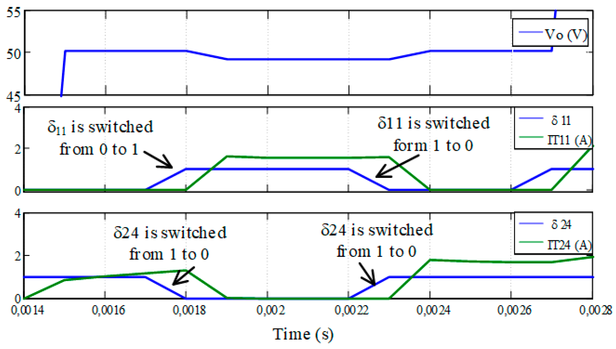
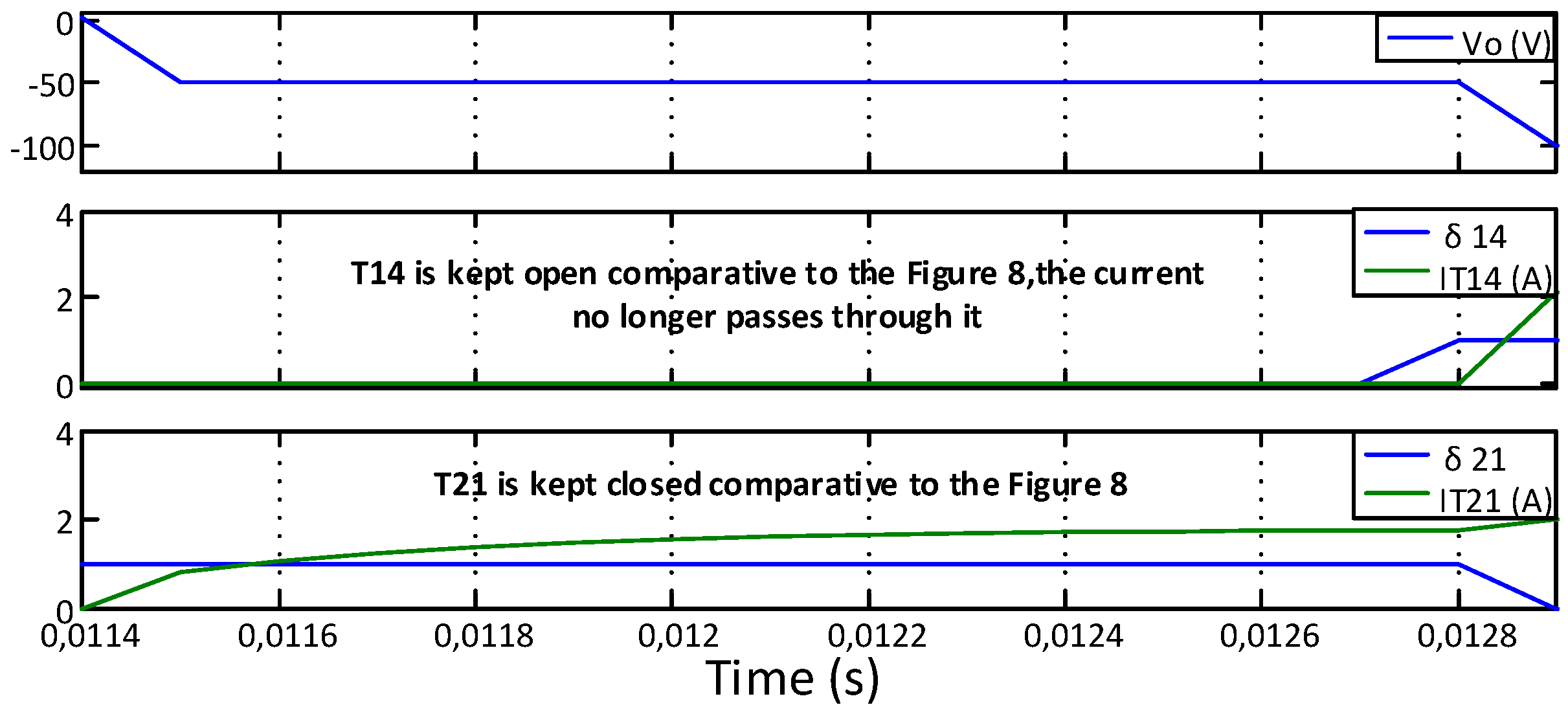
4. Simulation Results

To validate the performance of the proposed OPT-PWM applied to the HB-5L-NPC topology (Figure 2), some simulations were performed in the Matlab/Simulink environment using the SimPowerSystem library developed by MathWorks (Natick, MA, USA). The simulated system was the same as that illustrated in Figure 1 with an RL load and the OPT-PWM control. The parameters are presented in Table 1.
Figure 14 shows the output voltage when the converter is controlled by the proposed OPT-PWM. By comparing Figure 4 and Figure 14, it can be seen that the output voltage waveforms are the same. To verify the elimination of the unnecessary commutations on the Vdc/2 (and also −Vdc/2) level, the same zooms as in Figure 4 were performed.
Figure 15, Figure 16, Figure 17 and Figure 18 can be compared with Figure 6, Figure 7, Figure 8 and Figure 9. As can be observed, any commutation when the voltage level remains constant (equal at Vdc/2 and –Vdc/2) is no longer performed. Thus, the total number of commutations is decreased by 16 over one period.
To compare the proposed OPT-PWM and the classical LS-PWM, the operation of the system was tested for different switching frequencies while other parameters were kept unchanged. Table 4 shows the result when the system was operated under different switching frequencies. The THD of the injected current for the OPT-PWM is lower than for the LS-PWM at all frequencies. It should be mentioned that the proposed method always reduces the number of commutations, thus decreasing the switching losses in the system.

5. Experimental Results

To verify the validity of the proposed OPT-PWM control applied to the HB-5L-NPC, several experimental tests were carried out. The same parameters as those used in the simulations were considered. The test bench (Figure 19) was based on IGBT modules commercialized by the SEMIKRON Company (Nuremberg, Germany), reference SKM50GB123D. These IGBTs were driven by SKHI 22A drivers, distributed by the same company. The DC bus capacity value was 2200 µF.
The control method was applied by using a dSPACE system (Paderborn, Germany) containing a DS1005 control card as well as a DS2004 for high-resolution analog conversion (16 bit–0.8 μs) and a DS5101 PWM card with 12 outputs. The hardware implementation on the DS1005 was based on the modeling of the control algorithm carried out in the Matlab environment with classical blocks from the Simulink toolbox.
Some tests with a LS-PWM control were first performed and then the proposed OPT-PWM was applied to control the system. The results obtained from the two modulation strategies are compared in the following sections.

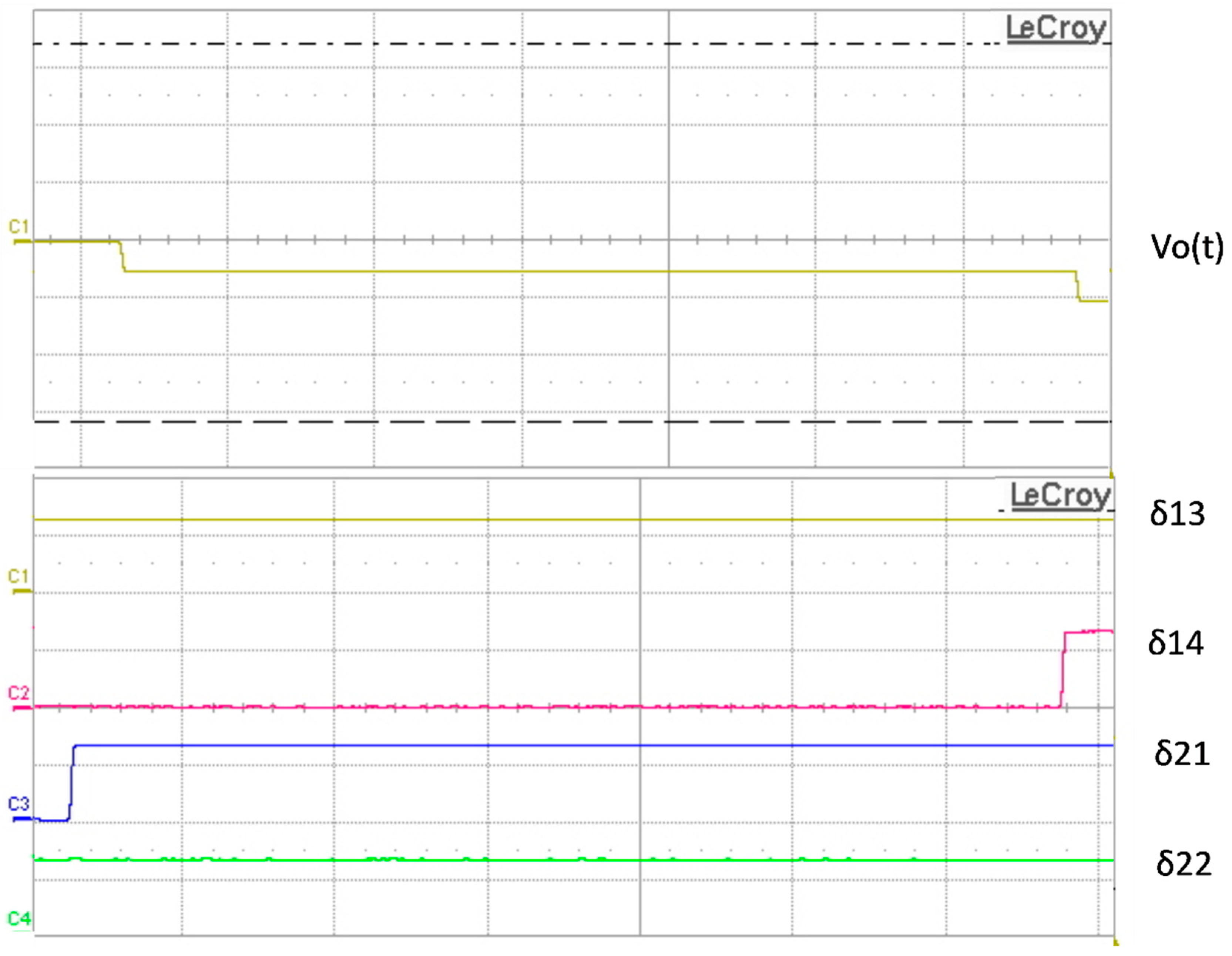
5.1. Experimental Results with LS-PWM Control

Figure 20 shows the output voltage of the converter with LS-PWM control. These results show clearly that there are the same small variations (peaks) at the same intervals as in the simulations. To confirm this, two zooms, one when the voltage remains a long time at Vdc/2 and the other at −Vdc/2, were made and are presented in Figure 21 and Figure 22.

5.2. Experimental Results with the Proposed OPT-PWM Control

Figure 23 shows the output voltage of the HB-5L-NPC converter with the proposed OPT-PWM control.
Figure 24 and Figure 25 show the experimental results for the OPT-PWM. As can be seen, there are no unnecessary commutations. This means that the goal of the proposed control was met: the advanced functionality for the modulation strategy that evaluates possible switching state trajectories and implements the trajectory that provides the minimal number of commutations is efficient.

6. Conclusions

This paper proposed an advanced PWM strategy applied to a five-level H-Bridge Neutral Point Clamped inverter. This modulation strategy optimizes the number of commutations without any degradation of the conventional PWM control performance. Both simulations and experimental tests were performed to confirm the validity of the proposed method. The results obtained with conventional PWM control (LS-PWM) and the proposed OPT-PWM control present similar output voltages for the HB-5L-NPC. The OPT-PWM results confirm that unnecessary commutations were removed.
By considering the number of commutations for each switch in simulations and experimental tests for two cases, thanks to the OPT-PWM control, the efficiency of the converter was improved. We note again that this advanced modulation strategy with reduced complexity can be applied to any modulation technique because its implementation uses an additional block.

Author Contributions

Investigation, F.B., P.P.; Resources, F.B., E.J. and P.P.; Writing—review and editing, F.B., E.J., P.P. and S.S.

Funding

This research received no external funding.

Conflicts of Interest

The authors declare no conflict of interest.

References

  1. Bouhali, O.; Rizoug, N.; Mesbahi, T.; Francois, B. Modeling and control of the three-phase NPC multilevel converter using an equivalent matrix structure. In Proceedings of the 7th IET International Conference on Power Electronics, Machines and Drives (PEMD 2014), Manchester, UK, 8–10 April 2014; pp. 1–6. [Google Scholar]
  2. Akagi, H. Multilevel Converters: Fundamental Circuits and Systems. Proc. IEEE 2017, 105, 2048–2065. [Google Scholar] [CrossRef]
  3. Nabae, A.; Takahashi, I.; Akagi, H. A New Neutral-Point-Clamped PWM Inverter. IEEE Trans. Ind. Appl. 1981, IA-17, 518–523. [Google Scholar] [CrossRef]
  4. Konstantinou, G.; Pou, J.; Capella, G.J.; Song, K.; Ceballos, S.; Agelidis, V.G. Interleaved Operation of Three-Level Neutral Point Clamped Converter Legs and Reduction of Circulating Currents Under SHE-PWM. IEEE Trans. Ind. Electron. 2016, 63, 3323–3332. [Google Scholar] [CrossRef]
  5. Barros, J.D.; Silva, J.F.A.; Jesus, É.G. Fast-predictive optimal control of NPC multilevel converters. IEEE Trans. Ind. Electron. 2013, 60, 619–627. [Google Scholar] [CrossRef]
  6. Behera, R.K.; Das, S.P. A forced switching technique for current controlled three-level NPC ac-dc converter. In Proceedings of the Joint International Conference on Power Electronics, Drives and Energy Systems (PEDES), New Delhi, India, 20–23 December 2010; pp. 1–6. [Google Scholar]
  7. Choudhury, A.; Pillay, P.; Williamson, S.S. DC-Bus Voltage Balancing Algorithm for Three-Level Neutral-Point-Clamped (NPC) Traction Inverter Drive With Modified Virtual Space Vector. IEEE Trans. Ind. Appl. 2016, 52, 3958–3967. [Google Scholar] [CrossRef]
  8. Kuo, C.C.; Tzou, Y.Y. FPGA predictive control for single-phase active NPC grid inverters with multi-sampling technique. In Proceedings of the Annual Conference of the IEEE Industrial Electronics Society (IECON 2016), Florence, Italy, 23–26 October 2016; pp. 2295–2300. [Google Scholar]
  9. Campanhol, L.B.G.; da Silva, S.A.O.; de Oliveira, A.A.; Bacon, V.D. Dynamic Performance Improvement of a Grid-Tied PV System Using a Feed-Forward Control Loop Acting on the NPC Inverter Currents. IEEE Trans. Ind. Electron. 2017, 64, 2092–2101. [Google Scholar] [CrossRef]
  10. Sebaaly, F.; Vahedi, H.; Kanaan, H.Y.; Moubayed, N.; Al-Haddad, K. Design and Implementation of Space Vector Modulation-Based Sliding Mode Control for Grid-Connected 3L-NPC Inverter. IEEE Trans. Ind. Electron. 2016, 63, 7854–7863. [Google Scholar] [CrossRef]
  11. Ebrahimi, J.; Karshenas, H. A New Single dc Source Six-Level Flying Capacitor Based Converter with Wide Operating Range. IEEE Trans. Power Electron. 2019, 34, 34–2158. [Google Scholar] [CrossRef]
  12. Stillwell, A.; Pilawa-Podgurski, R.C.N. A 5-Level Flying Capacitor Multi-Level Converter with Integrated Auxiliary Power Supply and Start-Up. In Proceedings of the IEEE Applied Power Electronics Conference and Exposition (APEC), Tampa, FL, USA, 26–30 March 2017; pp. 2932–2938. [Google Scholar] [CrossRef]
  13. Alamri, B.; Darwish, M. Power loss investigation in HVDC for cascaded h-bridge multilevel inverters (CHB-MLI). In Proceedings of the IEEE Eindhoven PowerTech, Eindhoven, The Netherlands, 29 June–2 July 2015; pp. 1–7. [Google Scholar] [CrossRef]
  14. Rojas, C.A.; Kouro, S.; Edwards, D.; Bin, W.; Rivera, S. Five-level H-bridge NPC central photovoltaic inverter with open-end winding grid connection. In Proceedings of the Conference of the IEEE Industrial Electronics Society (IECON 2014), Dallas, TX, USA, 29 October–1 November 2014; pp. 4622–4627. [Google Scholar] [CrossRef]
  15. Fan, S.; Zhang, K.; Xiong Jand Xue, Y. An Improved Control System for Modular Multilevel Converters with New Modulation Strategy and Voltage Balancing Control. IEEE Trans. Power Electron. 2015, 30, 358–371. [Google Scholar] [CrossRef]
  16. Rodriguez, J.; Bernet, S.; Steimer, P.K.; Lizama, I.E. A Survey on Neutral-Point-Clamped Inverters. IEEE Trans. Ind. Electron. 2010, 57, 2219–2230. [Google Scholar] [CrossRef]
  17. Hasan, N.S.; Rosmin, N.; Osman DA, A.; Musta’amal, A.H. Reviews on multilevel converter and modulation techniques. Renew. Sustain. Energy Rev. 2017, 80, 163–174. [Google Scholar] [CrossRef]
  18. Marquardt, R. Modular Multilevel Converters—Sate of the art and future progress. IEEE Power Electron. Mag. 2018, 5, 24–31. [Google Scholar] [CrossRef]
  19. Kobravi, K.; Iravani, R. A novel modulation strategy to minimize the number of commutation processes in the matrix converter. In Proceedings of the 2010 IEEE Energy Conversion Congress and Exposition, Atlanta, GA, USA, 12–16 September 2010. [Google Scholar]
  20. Yusuke, A.; Takeshita, T. PWM control of matrix converter for reducing a number of commutations and output voltage harmonics. In Proceedings of the 2007 Power Conversion Conference, Nagoya, Japan, 2–5 April 2007; pp. 769–775. [Google Scholar]
  21. Calle-Prado, A.; Alepuz, S.; Bordonnau, J.; Cortes, P.; Rodriguez, J. Predictive control of a back-to-back NPC converter-based wind power system. IEEE Trans. Ind. Electron. 2016, 63, 4615–4627. [Google Scholar] [CrossRef]
  22. Durand, C.; Klinger, M.; Coutellier, D.; Naceur, H. Power cycling reliability of power module: A survey. IEEE Trans. Device Mater. Reliab. 2016, 16, 80–97. [Google Scholar] [CrossRef]
  23. Niu, H. A review of power cycle driven fatigue, aging and failure modes for semiconductors power module. In Proceedings of the 2017 IEEE International Electrical Machines and Drives Conference, Miami, FL, USA, 21–24 May 2017; pp. 1–8. [Google Scholar]
  24. Ounejjar, Y.; AL-Haddad, K. Current control of the three phase five-level PUC-NPC converter. In Proceedings of the 38th Annual Conference on IEEE Industrial Electronics Society (IECON 2012), Montreal, QC, USA, 25–28 October 2012; pp. 4949–4954. [Google Scholar] [CrossRef]
  25. Song, W.; Feng, X.; Xiong, C. A neutral point voltage regulation method with SVPWM control for single-phase three-level NPC converters. In Proceedings of the IEEE Vehicle Power and Propulsion Conference (VPPC2008), Harbin, China, 3–5 September 2008; pp. 1–4. [Google Scholar] [CrossRef]
  26. Li, J.; Liu, Y.; Bhattacharya, S.; Huang, A.Q. An optimum PWM Strategy for 5-level active NPC (ANPC) converter based on real-time solution for THD minimization. In Proceedings of the IEEE Energy Conversion Congress and Exposition, San Jose, CA, USA, 20–24 September 2009; pp. 1976–1982. [Google Scholar] [CrossRef]
  27. Song, K.; Konstantinou, G.; Mingli, W.; Acuna, P.; Aguilera, R.P.; Agelidis, V.G. Windowed SHE-PWM of Interleaved Four-Quadrant Converters for Resonance Suppression in Traction Power Supply Systems. IEEE Trans. Power Electron. 2017, 32, 7870–7881. [Google Scholar] [CrossRef]
Figure 1. Studied system based on an five-level H-Bridge Neutral Point Clamped (HB-5L-NPC) inverter.
Electronics 08 00454 g001
Figure 2. (a) Three-level NPC topology (for one phase); (b) HB-5L-NPC topology (for one phase).
Electronics 08 00454 g002
Figure 3. Switching pattern generation by classical Level Shift Pulse Width Modulation (LS-PWM): (a) block diagram; (b) switching orders and the output voltage Vo(t).
Electronics 08 00454 g003
Figure 4. Zooms of the output voltage of the HB-5L-NPC.
Electronics 08 00454 g004
Figure 5. HB-5L-NPC converter configurations to generate the five voltage levels.
Electronics 08 00454 g005
Figure 6. Output voltage Vo(t), currents IT11 and IT24, and command of the switches T11 and T24 (Zoom 1).
Electronics 08 00454 g006
Figure 7. Output voltage Vo(t), currents IT11 and IT24, and command of the switches T11 and T24 (Zoom 2).
Electronics 08 00454 g007
Figure 8. Output voltage Vo(t), currents IT21 and IT14, and command of the switches T21 and T14 (Zoom 3).
Electronics 08 00454 g008
Figure 9. Output voltage Vo(t), currents IT21 and IT14, and command of the switches T21 and T14 (Zoom 4).
Electronics 08 00454 g009
Figure 10. Scheme of the proposed OPT-PWM control strategy.
Electronics 08 00454 g010
Figure 11. Search for the minimal number of commutations.
Electronics 08 00454 g011
Figure 12. States of switching and associated trajectories when i(t) is positive.
Electronics 08 00454 g012
Figure 13. The final algorithm for OPTimized (OPT)-PWM.
Electronics 08 00454 g013
Figure 14. Output voltage of the converter with the proposed OPT-PWM control.
Electronics 08 00454 g014
Figure 15. Voltage Vo, currents IT11 and IT24, and switching patterns δ11 and δ24 (Zoom 1).
Electronics 08 00454 g015
Figure 16. Voltage Vo, currents IT11 and IT24, and switching patterns δ11 and δ24 (Zoom 2).
Electronics 08 00454 g016
Figure 17. Voltage Vo, currents IT21 and IT14, and switching patterns δ21 and δ14 (Zoom 3).
Electronics 08 00454 g017
Figure 18. Voltage Vo, currents IT21 and IT14, and switching patterns δ21 and δ14 (Zoom 4).
Electronics 08 00454 g018
Figure 19. Experimental test bench.
Electronics 08 00454 g019
Figure 20. Output voltage of the converter with LS-PWM control.
Electronics 08 00454 g020
Figure 21. Output voltage Vo(t) and switching patterns sent to T11, T12, T23, and T24 (ZOOM 1 in Figure 20).
Electronics 08 00454 g021
Figure 22. Output voltage Vo(t) and switching patterns sent to T11, T12, T23, and T24 (ZOOM 2 in Figure 20).
Electronics 08 00454 g022
Figure 23. Output voltage during OPT-PWM control.
Electronics 08 00454 g023
Figure 24. Output voltage Vo(t) and switching patterns sent to T11, T12, T23, and T24 (ZOOM 1 of Figure 23).
Electronics 08 00454 g024
Figure 25. Output voltage Vo(t) and switching patterns sent to T13, T14, T21, and T22 (ZOOM 2 of Figure 23).
Electronics 08 00454 g025
Table 1. Simulation parameters.
SymbolQuantity
Vdc100 V
R27.7 Ω
L9 mH
fpwm1 kHz
m0.8
Table 2. Possible voltage levels and states for the single-phase HB-5L-NPC topology.
Vo*i(t) > 0i(t) < 0
StatesPassing ComponentStatesPassing Components
VdcS1T11, T12, T23, T24S10D11, D12, D23, D24
Vdc/2S2DC1+, T12, T23, T24S11D11, D12, T22, DC2+
S3T11, T12, T23, DC2−S12DC1−, T13, D23, D24
0S4DC1+, T12, T23, DC2−S13DC1−, T13, DC2+, T22
S5T23, T24, D14, D13S14D11, D12, T21, T22
S6T11, T12, D22, D21S15T13, T14, D23, D24
−Vdc/2S7D13, D14, DC2−, T23S16T13, T14, T22, DC2+
S8DC1+, T12, D21, D22S17DC1−, T13, T21, T22
−VdcS9D13, D14, D21, D22S18T13, T14, T21, T22
Table 3. Transitions and possible trajectories when passing from one voltage level to another (Case where i(t) > 0).
Initial Output Voltage LevelFinal Output Voltage LevelSelected Trajectories
Vo = VdcVo = Vdc/2S1 → S2
S1 → S3
Vo = VdcVo = 0S1 → S4
S1 → S5
S1 → S6
Vo = VdcVo = −Vdc/2S1 → S5 → S8,
S1 → S6 → S7
Vo =VdcVo = −VdcS1 → S5 → S9
S1 → S6 → S9
Vo = Vdc/2Vo= 0S2 → S4
S3 → S4
Vo = Vdc/2Vo = −Vdc/2S2 → S4 → S7
S2 → S4 → S8
S2 → S5 → S8
S3 → S4 → S7
S3 → S4 → S8
S3 → S6 → S7
Vo = Vdc/2Vo = −VdcS2 → S5 → S9
S3 → S6 → S9
Vo = −VdcVo = 0S9 → S5
S9 → S6
Vo = −VdcVo = −Vdc/2S9 → S7
S9 → S8
Vo = −Vdc/2Vo = 0S7 → S6
S8 → S5
Table 4. Total Harmonic Distortion (THD) of the injected current at different frequencies for SPWM and OPT-PWM.
Frequency Current THD OPT-PWMCurrent THD LS-PWM
1 kHz7.17% 7.50%
2 kHz4.28%4.48%
3 kHz3.38%4.11%
4 kHz2.49%3.2%

