Implementation of ARINC 659 Bus Controller for Space-Borne Computers
by
 , ,
, ,
Shuang Jiang
1,2,*,† ,
,
Shibin Liu
1,*,†,
Chenguang Guo
1,2,*,†,
Xu Fan
2,
Teng Ma
3 and
Prayag Tiwari
3
1
School of Electronics and Information, Northwestern Polytechnical University, Xi’an 710072, China
2
Department of ASIC Design, Beijing Microelectronics Technology Institute, Beijing 100076, China
3
Department of Information Engineering, University of Padova, 35131 Padova, Italy
*
Authors to whom correspondence should be addressed.
†
These authors contributed equally to this work.
Electronics 2019, 8(4), 435; https://doi.org/10.3390/electronics8040435
Submission received: 4 March 2019
/
Revised: 7 April 2019
/
Accepted: 11 April 2019
/
Published: 16 April 2019
(This article belongs to the Section Systems & Control Engineering)
Abstract
:As one of the key technologies of Honeywell, the aeronautical radio incorporated (ARINC) 659 bus is popular in current space-borne computers. However, Honeywell does not design ARINC 659 bus controller separately, and there are only a few papers about FPGA-based ARINC 659 bus controllers. Accordingly, to promote the extremely high performance needs of space-borne computers, this paper designs an ARINC 659 bus controller chip which integrates two independent bus interface units (BIUs), one 8-bit MCU, and several peripheral interfaces (i.e., UART, SPI, and I2C). Because the two BIUs are identical and mutually checked, the symmetry problem is emphatically dealt with in the design of this bus controller, and effective timing convergence is realized, which makes the bus controller work reliably and stably. In addition, due to the circuit’s large scale, design for testability (DFT) is also considered. Accordingly, on-chip clock (OCC) and scanning compression test technique are used to realize the at-speed test and shorten the test time, respectively.
1. Introduction
Backplane bus is a communication network used to connect various functional plug-ins in a computer system. Backplane bus is commonly used in the commercial computing field, including PCI bus [1], Compact PCI bus [2], VME bus [3], etc. Meanwhile, the backplane bus applied in the field of industrial measurement and control is usually extended on the basis of the general backplane bus such as extending the PCI bus to the PXI bus [4] and the VME bus to the VXI bus [5]. With the development of the new generation integrated modular avionics (IMA) system [6], data communication between line replaceable modules (LRMs) requires higher reliability, high fault tolerance, and fault isolation of the system. Therefore, Honeywell proposed the ARINC 659 bus standard which provides the highest level of reliability, integrity, and redundancy among the currently used aviation data buses [7,8].
The ARINC 659 standard proposed by Honeywell was originally used in the SAFEbusTM of Boeing 777’s aircraft information management system (AIMS) [9]. Later, the ARINC 659 bus began to be used in the versatile integrated avionics (VIA) [10] of Boeing 717N, MD-10, KC-130, etc. Currently, the space-borne computers used in space explorations such as the highly reliable layered system (HRLS) of NASA [11] and the Shenzhou spacecraft of CASC [12], began to adopt the ARINC 659 bus. Unfortunately, as a proprietary core technology, Honeywell does not design the ARINC 659 bus controller separately, and so far only the FPGA-based ARINC 659 bus controllers which usually have large chip size and complex system can be found in the publication [13,14,15]. Since space explorations require extremely high performance of the ARINC 659 bus, and the ARINC 659 bus controller is popular in space-borne computer, it is necessary to design a fully customized ARINC 659 bus controller chip to improve the performance and miniaturization of the controller.
Moreover, for space-borne computers, the greater the function density, the more potential fault propagation paths. If parallel internal bus is used, there will be more fault propagation paths, which will reduce the reliability of the system. If distributed serial internal bus is used, such as the ARINC 659 bus, it can locate and isolate the error module effectively, which not only does not affect other normal modules, but also contributes to the subsequent system reconfiguration [7,15]. The ARINC 659 bus has many advantages, such as clear boundary between internal nodes, flexible bus architecture, convenient upgrading of hardware and software, 4-line cross check, double machine check, error silence tolerance, etc. It is easy to realize the robust partition in space and time and can realize the real-time switching of backup system. Accordingly, the ARINC 659 bus has become the most effective way to improve the management and data processing ability of current aerospace electronic system, and it is also a hot spot in the development of space-borne computer bus [9,10,11,12,13,14,15].
In the design of ARINC 659 bus controller, each LRM of the ARINC 659 bus needs two BIUs which forms a dual redundancy structure and accomplishes the main function of ARINC 659. The two BIUs are identical and mutually checked. Therefore, symmetry problem which will lead to worse timing convergence needs to be seriously considered. In addition, the scale of ARINC 659 bus controller chip is usually very large, the DFT problem also needs to be paid more attention.
This paper designs an ARINC 659 bus controller circuit, first to fill the gap in the design of the corresponding chip, second to improve the certainty and fault tolerance of space-borne computers by solving some key technologies, and third, to provide a novel architecture for ARINC 659 bus controller. The following paper is divided into three parts. Firstly, the architecture of the bus controller is proposed, then symmetry problem and DFT are emphatically dealt with. Finally, simulation results are analyzed.
2. Architecture of ARINC 659 Bus Controller
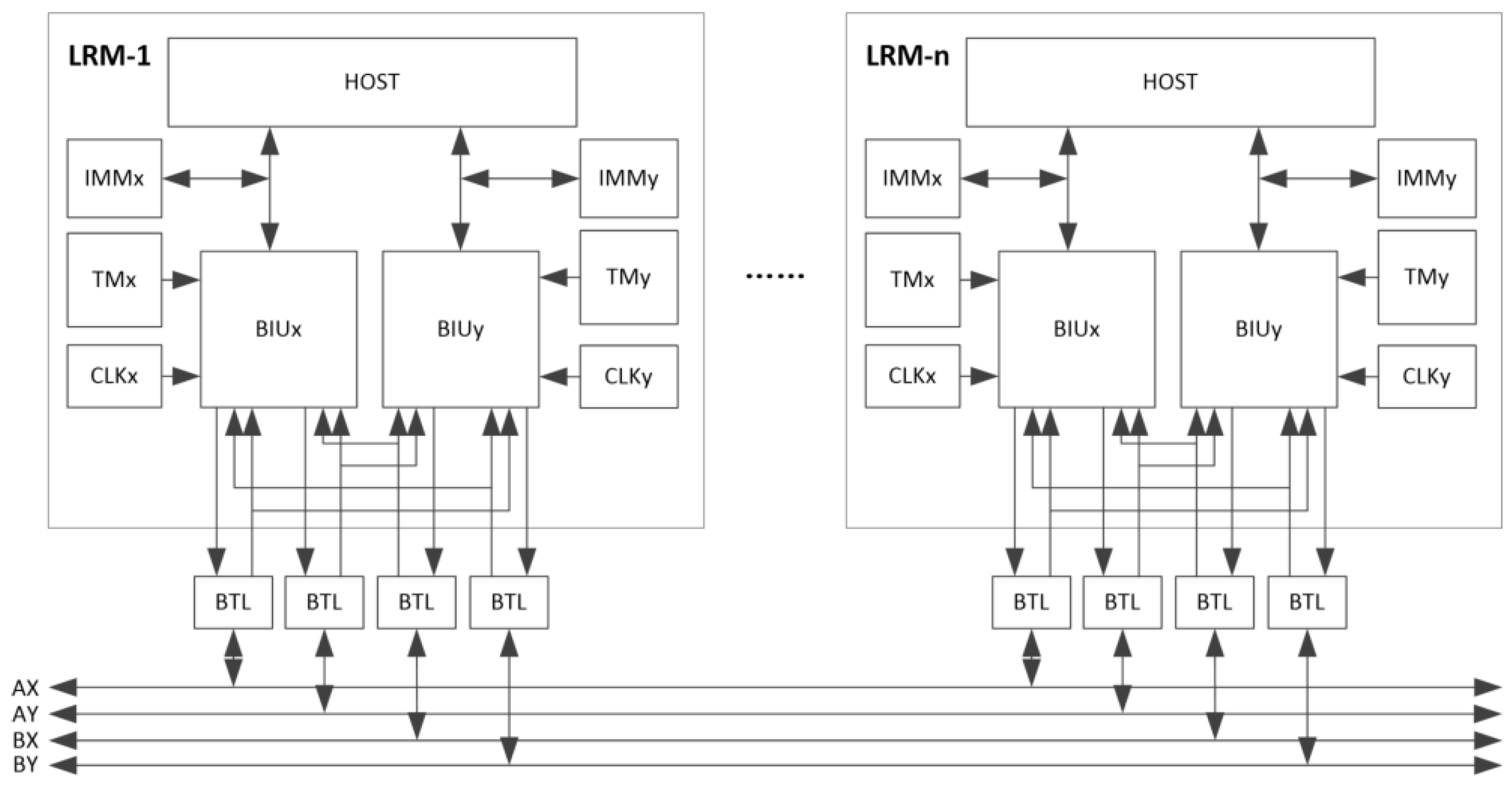
Based on the protocol of the ARINC 659, the schematic of the ARINC 659 bus is shown in Figure 1, including n LRMs, with a maximum value of 32 for the number n. The two BIUs which form a dual redundancy structure in each LRM interface to four buses (i.e., AX, AY, BX, and BY) for dual self-checking and transmitting data. The two inter module memories (IMM) in each LRM can realize the bus data interaction between HOST and BIUs, and the two crystal oscillators are provided to two BIU, respectively. Using two crystal oscillators can increase the redundancy of the circuit and reduce the possibility of failure caused by crystal oscillator. The sequences of commands using frame description language (FDL) are stored in the table memory (TM). The node communication on ARINC 659 bus adopts a high-speed backplane transceiver logic (BTL) which can support the rate of 30 Mbps on a single bus very well.
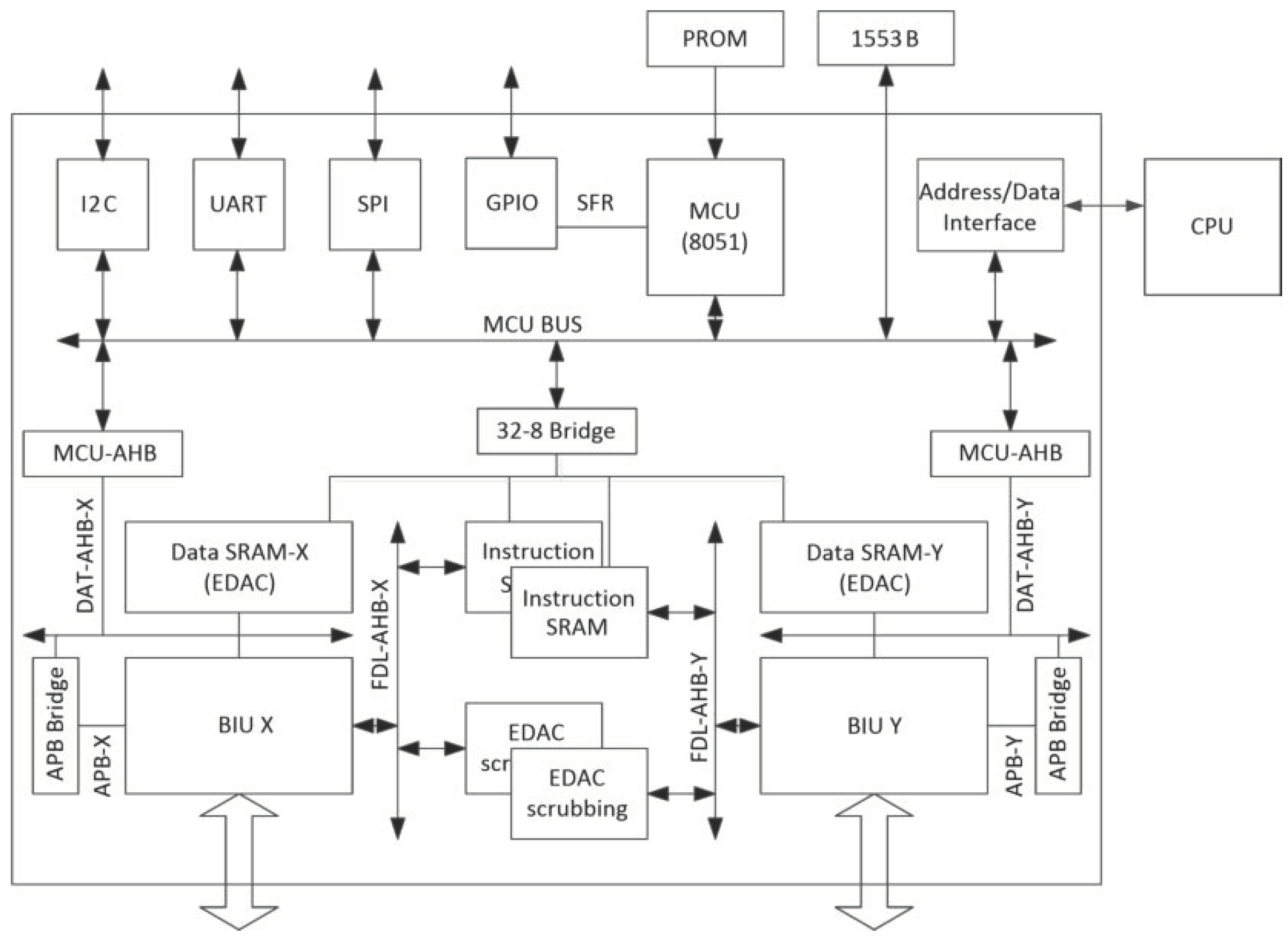
Accordingly, this paper presents a bus controller for ARINC 659, as shown in Figure 2. It can be seen from Figure 2 that the circuit can be controlled by external CPU and internal MCU (8051) respectively, which means that the chip has two working modes (i.e., CPU mode and MCU mode). The modes can be selected through the pin of the circuit.
In MCU mode, the on-chip MCU controls the working state of all other modules except BIUs and accomplishes the data exchange between the BIU cache and various interface controllers (e.g., UART, SPI, I2C, and GPIO) through the MCU bus. If it is in the main control board of the slave computer, the MCU also needs to communicate with the external 1553B controller, receive and execute commands sent by the computer over the 1553B bus. Normally, the two BIUs receive and send data from their respective instruction SRAM with FDL, read data from the dual-port data SRAM, and send data to the ARINC 659 bus according to the instructions, or get data from the bus and save it to data SRAM.
In CPU mode, through the address/data interface module, the instruction SRAM and data SRAM are exposed to CPU as an interface chip for external CPU to access the ARINC 659 bus. When the chip is powered up, the on-chip MCU or the external CPU needs to load the sequences of commands into the instruction SRAM. Because the two BIUs execute the same commands, the two instruction SRAM share the same address space and are write-only.
3. Key Technologies
3.1. Internal Clock Synchronization
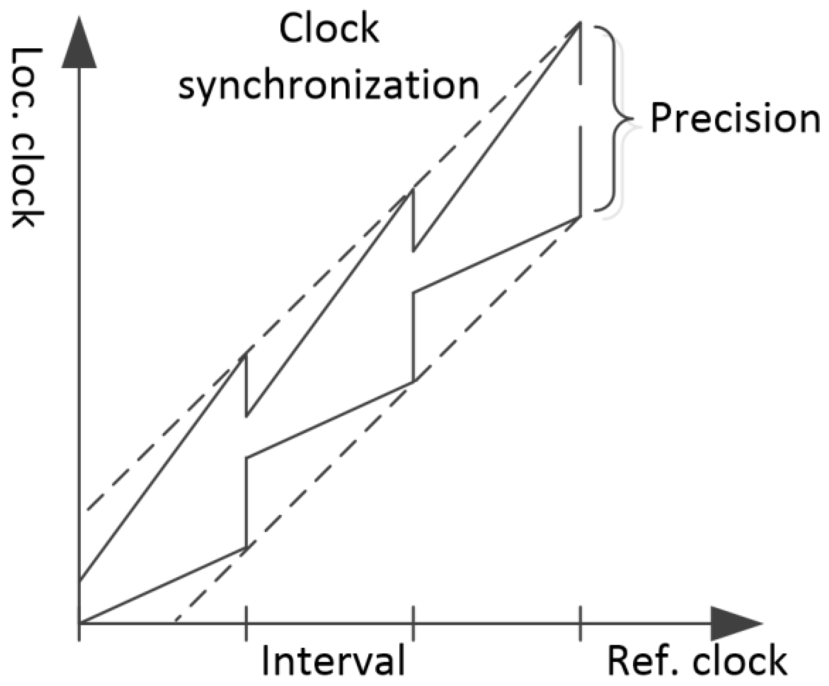
In space-borne computers, time can be divided into logical time and physical time. Since the task of space-borne computer is to interact with the physical world, the logical time to distinguish the sequence of events cannot meet the functional requirements. In addition, “external clock synchronization” with precise physical time, such as International Atomic Time (TAI), Coordinated Universal Time (UTC), or temperature-compensated crystal oscillator (TXCO), requires complex receivers or expensive advanced devices, and cannot be used to synchronize internal modules. Therefore, the synchronization between internal modules of a space-borne computer called “internal clock synchronization” is needed [16,17].
In this paper, the clock inputs of two BIUs of ARINC 659 bus controller are Clk_X and Clk_Y. Since Clk_X and Clk_Y are generated by their own crystal oscillator respectively, the requirement of clock synchronization between modules is generated. As shown in Figure 3, the local clock is regularly calibrated according to the reference clock. The clock accuracy of each module is ensured by correcting the shift of each crystal oscillator periodically.
3.2. Symmetric Structure
Symmetry problem is the main reason for the difficulty of time convergence [18,19]. According to ARINC 659 protocol, there are three kinds of timing skew between two BIUs, namely spatial skew, temporal skew, and XY skew [3].
Spatial skew is a skew caused by space factors such as position, capacitance, electrical characteristics of LRM backplane bus, etc. Temporal skew is the result of different transmission delays of different components on two LRMs. Both are independent of chip design. XY skew is the skew between two BIUs in one LRM after the latest resync pulse, which is the reflection of internal transmission delay and depends on the chip design. It is obvious that the minimization of XY skew in chip design will reduce the requirements for spatial skew and temporal skew.
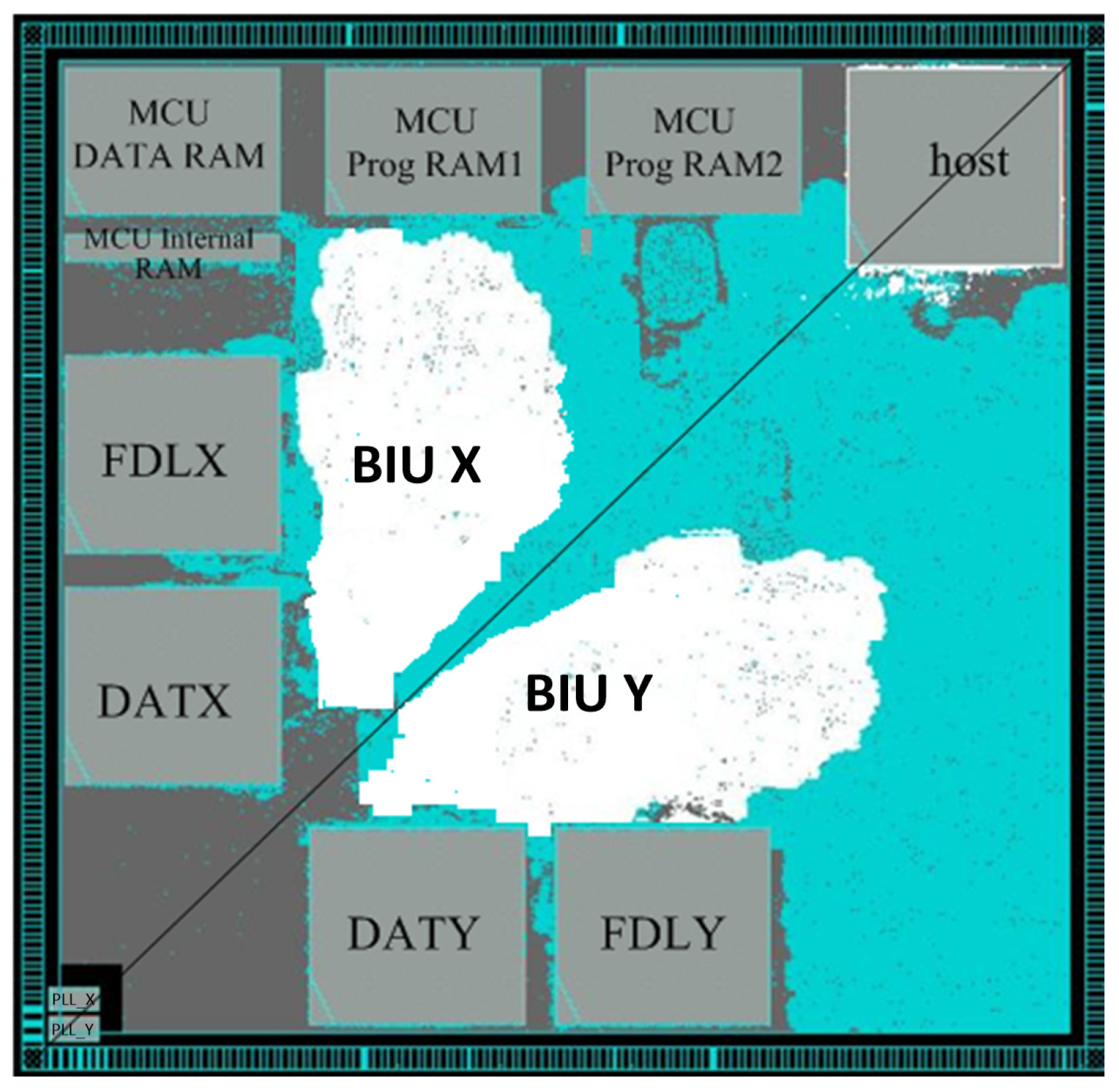
Within the circuit, the clock structure and logical composition of the two BIUs are identical, so the symmetrical structure of the two BIUs in the physical position can maximize the reduction of XY skew. Therefore, in the stage of pin arrangement and layout, it is necessary to distribute the two BIUs symmetrically along the 45-degree diagonal axis, as shown in Figure 4.
In the pin arrangement, the pin of the two BIUs is symmetrical relative to the 45-degree diagonal. In layout planning, the two PLLs (i.e., PLL_X and PLL_Y) are placed at the edge corner of the chip. The logic unit (i.e., BIU X and BIU Y), instruction SRAM (i.e., FDLX and FDLY) and data SRAM (i.e., DATX and DATY) of the two BIUs are distributed symmetrically based on the 45-degree diagonal line of the chip, so that the wiring of the two channels is completely consistent. Other IP modules are laid out according to the timing requirements.
3.3. On-Chip Clock (OCC) for at-Speed Test
The operating frequency of the controller is 120 MHz. Based on the following three considerations, it is necessary to adopt the on-chip clock (OCC) structure for at-speed test.
First of all, it can reduce the requirement of test equipment, which only needs to provide a low speed reference clock. Secondly, the test mode has a high probability of register flipping and high-power consumption. When OCC structure is used, shift clock is low frequency and only capture clock is high frequency, which can avoid the damage to the circuit caused by excessive power consumption. Finally, the manufacturing defects in deep submicron process can be found in the at-speed test as a supplement to the stuck-at fault test [20]. The OCC structure can be automatically inserted with DFT Compiler, and its timing waveform is shown in Figure 5.
The main part of OCC is the OCC controller, which is essentially a slow and fast clock switching mux with less glitch. When the scan_enable is 1, the scan chain is in the shift state, the slow ATEclk input is used as the clock of the register. When the scan_enable is 0, the scan chain is in the capture state, two clock pulses generated by PLLs are used as capture clocks. One is for launch clock, and the other is for capture clock.
3.4. Scanning Compression Test
For the following two considerations, the controller in this paper uses the scanning compression test technology. Firstly, due to the large circuit size and the large number of registers, the length of scan chain can be shortened to save test time and reduce test cost. Secondly, due to the limited number of ports, it is impossible to define enough ports for testing. The decompressor and compressor are generated by DFT Compiler when inserting the scan chain.
4. Simulation Results
4.1. Time Convergence Analysis
The crystal oscillator with clock precision of 50 ppm and output frequency of 30 MHz is used in this paper, which means the operating frequency of the proposed controller is 120 MHz. For the crystal oscillator used in this paper, the offset per cycle is 1.665 × 10⁻³ ns and the maximum number of clock cycles required to transmit a message is 4105, so the maximum deviation for a message is 6.835 ns. Since the estimation of the skew is 1 ns for spatial skew and 4.167 ns for temporal skew, the maximum of XY skew is 1.668 ns. The simulation results below are based on 0.18 µm CMOS process library.
There are four buses (i.e., AX, AY, BX, and BY) for the bus interface of the controller. Each bus contains one clock signal and 2-bit serial data (i.e., d0 and d1). Accordingly, the four buses have 12 signals. In addition, the input and output of each bus are independent, so the total signals are 24 (i.e., axck, axd0, axd1, bxck, bxd0, bxd1, ayck, ayd0, ayd1, byck, byd0, byd1, oaxck, oaxd0, oaxd1, obxck, obxd0, obxd1, oayck, oayd0, oayd1, obyck, obyd0, and obyd1).
For the performance of timing convergence, the realization of symmetry problem in different paths needs to be considered, including:
- (1)
- The symmetry from the reference clock to the two PLLs;
- (2)
- Clock tree symmetry;
- (3)
- Symmetry from the bus input signals to the first stage registers;
- (4)
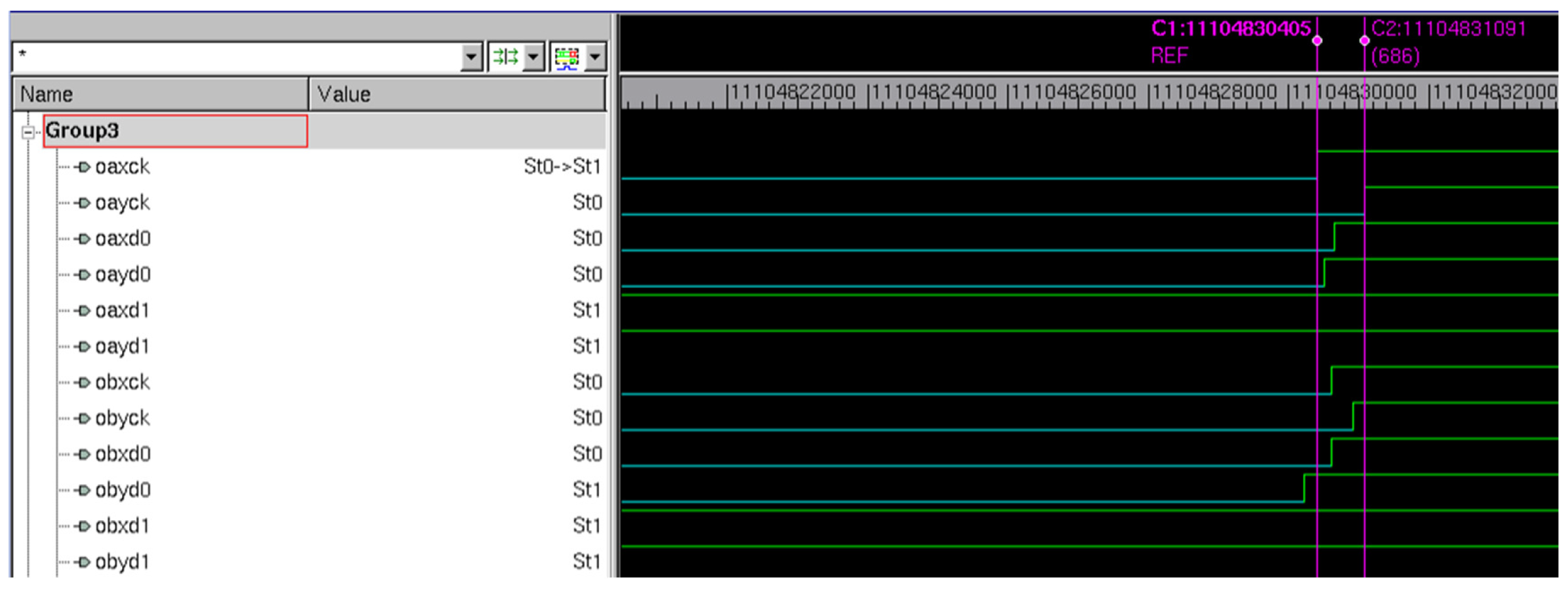
- Symmetry between the output bus signals of the two BIUs.
When the symmetry of the above four paths is insufficient, it will lead to the inconsistency of the two working states, the asynchronous operation of the bus, and even the abnormal operation of the bus. After simulation with VCS tool with the MAX process corner, the simulation results of the input signals are shown in Table 1.
It can be seen from Table 1 that the symmetry deviation between BIU X and BIU Y is within 0.3 ns under the MAX process corner, which means that the deviation is smaller at the MIN process corner.
4.2. DFT Analysis
Using 0.18 µm CMOS process, the controller’s size is 13.4 mm × 13.2 mm, which is smaller than the corresponding FPGA used in reference x and y. Therefore, the DFT needs to be considered. As mentioned above, the proposed circuits support two kinds of test to improve test flexibility. The at-speed test is a supplement to the stuck-at fault test.
As shown in Table 3, the corresponding faults in DFT analysis can be classified into five categories: Detected (DT), Possibly detected (PT), Undetectable (UD), ATPG untestable (AU), and Not detected (ND). For the stuck-at fault test, the scanning test coverage of the controller is 98.47%. For the at-speed test, the scanning test coverage of the controller is 87.68%.
Before compression, there are nine scan chains in the controller, with which the maximum number of registers in the scan chain is 12,873. After compression, the nine scan chains become 74 scan chains, and the maximum number of registers in the scan chain is not more than 400, so the test time can be changed to nearly 1/32 of the original value.
5. Conclusions
This paper shows a better solution to the symmetry problem and DFT problem when designing a fully customized ARINC 659 bus controller chip for space-borne computers. Based on the 0.18 µm CMOS process library, the operating frequency of the proposed controller is 120 MHz and the size of the chip is 13.4 mm × 13.2 mm. When used in a space-borne computer, it poses a great challenge to the time convergence and reliability. The proposed design of symmetric structure makes time convergence better, while the proposed DFT design makes the controller more reliable. As a distributed high-speed serial internal bus, the proposed bus controller can not only be applied to space-borne computer communication, but also can meet the development trend of space-borne integrated electronic technology in the future.
Author Contributions
Conceptualization, S.J., S.L. and C.G.; Formal analysis, S.J., S.L., C.G., X.F., T.M. and P.T.; Methodology, S.J., S.L. and C.G.; Writing—original draft, S.J. and C.G.; Writing—review & editing, S.L., X.F., T.M. and P.T.
Funding
This research received no external funding.
Conflicts of Interest
The authors declare no conflict of interest.
References
- Bohm, P. Incremental and Verified Modeling of the PCI Express Protocol. IEEE Trans. Comput.-Aided Des. Integr. Circuits Syst. 2010, 29, 1495–1508. [Google Scholar] [CrossRef]
- Li, Z.; Hu, X. An extension HA design for the hot-swap application of Compact PCI device. In Proceedings of the 2013 IEEE 8th Conference on Industrial Electronics and Applications (ICIEA), Melbourne, Australia, 19–21 June 2013; pp. 646–650. [Google Scholar] [CrossRef]
- Yin, H.; Fu, P.; Wang, B. Design of the VME Bus Controller Module Based on ARM. In Proceedings of the 2016 Sixth International Conference on Instrumentation & Measurement, Computer, Communication and Control (IMCCC), Harbin, China, 21–23 July 2016; pp. 193–196. [Google Scholar] [CrossRef]
- Lu, C.L.; Zhang, G.; Du, C.T.; Cheng, J.H.; Chen, X.F. Design of closed-loop feedback control system based on PXI bus. In Proceedings of the 2017 IEEE 2nd Information Technology, Networking, Electronic and Automation Control Conference (ITNEC), Chengdu, China, 15–17 December 2017; pp. 1655–1658. [Google Scholar] [CrossRef]
- Li, M.; Liang, G.; Gao, Q. Design and implementation of VXI bus Arbitrary Waveform Generator. In Proceedings of the 2012 International Conference on Systems and Informatics (ICSAI2012), Yantai, China, 19–21 May 2012; pp. 1295–1297. [Google Scholar] [CrossRef]
- Kornek-Percin, B.; Petersen, B.; Reichle, M.; Bader, J. New IMA architecture approach based on IMA resources. In Proceedings of the 2015 IEEE/AIAA 34th Digital Avionics Systems Conference (DASC), Prague, Czech Republic, 13–17 September 2015; pp. 6A2-1–6A2-8. [Google Scholar] [CrossRef]
- Carpenter, D.; Hoyme, C. ARINC 659 scheduling: Problem definition. In Proceedings of the 1994 Real-Time Systems Symposium, San Juan, PR, USA, 7–9 December 1994; pp. 165–169. [Google Scholar] [CrossRef]
- ARINC Backplane Data Bus. Available online: https://standards.globalspec.com/std/514584/arinc-659 (accessed on 24 February 2019).
- Michael, J.M. Boeing B-777. In The Avionics Handbook; Spitzer, C.R., Ed.; Boca Ratonby by CRC Press LLC: Boca Raton, FL, USA, 2001; p. 29. [Google Scholar]
- Sutterfield, B.; Hoschette, J.A.; Anton, P. Future integrated modular avionics for jet fighter mission computers. In Proceedings of the 2008 IEEE/AIAA 27th Digital Avionics Systems Conference, St. Paul, MN, USA, 26–30 October 2008; pp. 1.A.4-1–1.A.4-11. [Google Scholar] [CrossRef]
- Black, R.; Fletcher, M. Next generation space avionics: A highly reliable layered system implementation. In Proceedings of the 23rd Digital Avionics Systems Conference (IEEE Cat. No. 04CH37576), Salt Lake City, UT, USA, 28 October 2004; pp. 13.E.4-1–13.E.4-15. [Google Scholar] [CrossRef]
- Shenzhou (Spacecraft). Available online: https://en.wikipedia.org/wiki/Shenzhou_(spacecraft) (accessed on 7 April 2019).
- Abbas, G.G.; Zhu, Y.; Muhammad, A.H.; Waqar, A.; An, J. Backplane bus controller implementation in Fpga for hard real time control systems. In Proceedings of the 2011 IEEE 3rd International Conference on Communication Software and Networks, Xi’an, China, 27–29 May 2011; pp. 451–456. [Google Scholar] [CrossRef]
- Muhammad, A.H.; Fan, X.; Abbas, G.G.; Waqar, A.; An, J. Implementation of data transfer and synchronous pulse operation for ARINC 659. In Proceedings of the 2011 IEEE 3rd International Conference on Communication Software and Networks, Xi’an, China, 27–29 May 2011; pp. 485–489. [Google Scholar] [CrossRef]
- Ahmad, W.; Shengbing, Z.; Amjad, H.M.; Gillani, G.A.; Jianfeng, A. FPGA based real time implementation scheme for ARINC 659 backplane data bus. In Proceedings of the 2011 3rd International Conference on Computer Research and Development, Shanghai, China, 11–13 March 2011; pp. 478–482. [Google Scholar] [CrossRef]
- Wedde, H.F.; Freund, W. Harmonious internal clock synchronization. In Proceedings of the 12th Euromicro Conference on Real-Time Systems, Stockholm, Sweden, 19–21 June 2000; pp. 175–182. [Google Scholar] [CrossRef]
- Chaudhuri, S.; Nandy, S. A modified physical clock synchronization algorithm. In Proceedings of the 2013 3rd IEEE International Advance Computing Conference (IACC), Ghaziabad, India, 22–23 Febuary 2013; pp. 34–39. [Google Scholar] [CrossRef]
- Matsumoto, F.; Matsuo, S.; Nishioka, S.; Abe, H.; Ohbuchi, T. Study on offset reduction method for a fully differential filter employing symmetrical floating impedance scaling circuits. In Proceedings of the 2016 International Symposium on Intelligent Signal Processing and Communication Systems (ISPACS), Phuket, Thailand, 24–27 October 2016; pp. 1–5. [Google Scholar] [CrossRef]
- Ai, Z.; Wang, L.; Liu, G.; Xu, C. A method of multi-channel pulse acquisition synchronization. In Proceedings of the 2017 International Conference on Circuits, System and Simulation (ICCSS), London, UK, 14–17 July 2017; pp. 176–179. [Google Scholar] [CrossRef]
- DFTMAX Ultra. Available online: https://www.synopsys.com (accessed on 24 February 2019).
Figure 1.
Schematic of the ARINC 659 bus.

Figure 2.
Architecture of the proposed bus controller.

Figure 3.
Clock synchronization between modules.

Figure 4.
Layout of the proposed bus controller.

Figure 5.
Timing waveform of on-chip clock (OCC).

Figure 6.
Symmetry between the output bus signals of the two bus interface units (BIUs).


Table 1.
Simulation results of the input bus signals.
| Path | BIU X | BIU Y | Deviation |
|---|---|---|---|
| Ref. clock to First stage Reg. | 4.05 ns | 4.07 ns | 0.02 ns |
| axck/ayck to First stage Reg. | 5.94 ns | 5.83 ns | 0.11 ns |
| axd0/ayd0 to First stage Reg. | 5.88 ns | 5.88 ns | 0 ns |
| axd1/ayd1 to First stage Reg. | 5.66 ns | 5.96 ns | 0.30 ns |
| bxck/byck to First stage Reg. | 5.72 ns | 5.96 ns | 0.24 ns |
| bxd0/byd0 to First stage Reg. | 5.72 ns | 5.64 ns | 0.08 ns |
| bxd1/byd1 to First stage Reg. | 5.62 ns | 5.76 ns | 0.14 ns |
Table 2.
Simulation results of the output bus signals.
| Path | Deviation |
|---|---|
| Path Deviation oaxck-oayck | 0.686 ns |
| oaxd0-oayd0 | 0.144 ns |
| oaxd1-oayd1 | 0.376 ns |
| obxck-obyck | 0.322 ns |
| obxd0-obyd0 | 0.390 ns |
| obxd1-obyd1 | 0.335 ns |
Table 3.
Test results of the proposed controller.
| Test Type | DT | PT | UD | AU | ND | Total Faults | Test Coverage |
|---|---|---|---|---|---|---|---|
| Stuck-at fault test | 1,736,637 | 828 | 23,550 | 26,551 | 32 | 1,787,598 | 98.47% |
| At-speed test | 1,373,130 | 42 | 3153 | 0 | 192,849 | 1,569,174 | 87.68% |
© 2019 by the authors. Licensee MDPI, Basel, Switzerland. This article is an open access article distributed under the terms and conditions of the Creative Commons Attribution (CC BY) license (http://creativecommons.org/licenses/by/4.0/).
Share and Cite
MDPI and ACS Style
Jiang, S.; Liu, S.; Guo, C.; Fan, X.; Ma, T.; Tiwari, P. Implementation of ARINC 659 Bus Controller for Space-Borne Computers. Electronics 2019, 8, 435. https://doi.org/10.3390/electronics8040435
AMA Style
Jiang S, Liu S, Guo C, Fan X, Ma T, Tiwari P. Implementation of ARINC 659 Bus Controller for Space-Borne Computers. Electronics. 2019; 8(4):435. https://doi.org/10.3390/electronics8040435
Chicago/Turabian StyleJiang, Shuang, Shibin Liu, Chenguang Guo, Xu Fan, Teng Ma, and Prayag Tiwari. 2019. "Implementation of ARINC 659 Bus Controller for Space-Borne Computers" Electronics 8, no. 4: 435. https://doi.org/10.3390/electronics8040435
Note that from the first issue of 2016, this journal uses article numbers instead of page numbers. See further details here.