Article

Design, Simulation and Hardware Implementation of Shunt Hybrid Compensator Using Synchronous Rotating Reference Frame (SRRF)-Based Control Technique

by
R. Balasubramanian
,
K. Parkavikathirvelu
,
R. Sankaran
and
Rengarajan Amirtharajan
*
School of Electrical & Electronics Engineering (SEEE)S, SASTRA Deemed University, Thirumalaisamudram, Thanjavur 613401, India
*
Author to whom correspondence should be addressed.
Electronics 2019, 8(1), 42; https://doi.org/10.3390/electronics8010042
Submission received: 26 September 2018 / Revised: 17 December 2018 / Accepted: 21 December 2018 / Published: 1 January 2019
(This article belongs to the Special Issue Applications of Power Electronics)

Abstract

:
This paper deals with the design, simulation, and implementation of shunt hybrid compensator to maintain the power quality in three-phase distribution networks feeding different types balanced and unbalanced nonlinear loads. The configuration of the compensator consists of a selective harmonic elimination passive filter, a series-connected conventional six-pulse IGBT inverter, acting as the active filter terminated with a DC link capacitor. The theory and modelling of the compensator based on current harmonic components at the load end and their decomposition in d-q axis frame of reference are utilized in the reference current generation algorithm. Accordingly, the source current waveform is made to follow the reference current waveform using a high-frequency, carrier-based controller. Further, this inner current control loop is supported by a slower outer voltage control loop for sustaining desirable DC link voltage. Performance of the compensator is evaluated through MATLAB simulation covering different types of loads and reduction of harmonic currents and THD at the supply side along with excellent regulation of DC link voltage are confirmed. The performance of a hybrid compensator designed and fabricated using the above principles is evaluated and corroborated with the simulation results.

1. Introduction

One major area of research that has gained attention in recent times is maintaining power quality of distribution systems. The power quality issues arise due to the widespread usage of processed power in industrial applications and commercial/domestic applications [1,2,3]. For example, variable speed drives are implemented through power modulators which consist of high-power controlled/uncontrolled rectifiers feeding variable voltage and variable frequency multiphase inverters. Similarly, commercial power consumption is characterised by appliances like computers, photocopiers, and fax machines, along with fluorescent and CFL lamps. All the above represent nonlinear loads, resulting in lower supply-side power factor and waveform distortion, indicated by harmonic components in voltage and current. The adverse effect of harmonics includes heating and extra losses, saturation and malfunctioning of distribution transformers, interference with communication signals, damages to consumer utilities, and in extreme cases, the failure of supply-side equipment [4].
The initial steps towards mitigation of the above problems were focused on the low power factor at the supply side only, whereby a passive power filter (PPF) connected in shunt compensates for the lagging reactive current, which was extended with selective harmonic elimination. The disadvantage of this approach is insensitivity with load current changes and fluctuations in supply-side voltage. The filter performance also depends on the load power factor, which may be variable. For example, in [5], the load is a motor that can work at different conditions. As a means of overcoming these problems, various active compensator topologies comprising of series and shunt elements have been proposed which have gained wide acceptance. However, some of the disadvantages, like high initial and operating cost due to the use of high-rating semiconductors and also the need for maintaining a high DC link voltage, have limited the application of pure shunt active power filter in medium- and high-power installations [6,7]. As a result, the stage was set for development of shunt hybrid power filters (HPFs), which represent a judicious combination of both passive and active power filters (APFs). The various hybrid compensator configurations are: (i) series active power filter and shunt passive power filter, (ii) shunt active power filter and shunt passive power filter and (iii) a series combination of passive power filter and active power compensator connected in shunt with the system. The series element in configuration (i) has to be rated for maximum load current and is not flexible for many applications. The configuration (ii) with two independent compensators in parallel requires both blocks to be rated at the supply voltage leading to high DC link capacitor voltage rating [8,9,10].
In comparison, the third topology where the passive power filter elements appear in series with the standard active power filter circuitry poses important advantages in terms of reflecting nearly zero impedance of the passive power filter for load current harmonics and at the same time high impedance for system side voltage harmonics. Further, it leads to absorbing the fundamental voltage component across the passive power filter, thereby reducing the voltage rating of the DC link capacitor to only the harmonic components which are to be suppressed. Accordingly, the rating and cost of the capacitor and the power semiconductor switches in the compensator are considerably reduced [8]. Further, this topology is effective in preventing system resonance, reducing switching noise and avoidance of any circulating current in the compensator.
The control requirements for all configurations involving active power filter boil down to the generation of reference current waveform, switching and triggering timings for semiconductor switches to match the source current and also for maintaining the desired voltage across the DC link capacitor. Accordingly, a variety of control schemes supported by related algorithms have been reported in the literature [11,12,13,14,15,16,17,18,19,20]. Time domain methods provide fast response, compared with frequency domain methods. Accordingly, many authors have proposed control techniques such as instantaneous reactive power theory, synchronous rotating reference frame (SRRF) theory, sliding mode controller, neural network techniques and feedforward control to improve the performance of both active as well as hybrid filters.
In this paper, the third topology has been utilised, where the passive power filter is designed with the aim of 5th and 7th selective harmonic elimination along with an active power compensator connected in series. The active component of the compensator is modelled in the stationary abc frame of mains and further transformed to the rotating dq frame to avoid time dependence of parameters to reduce the control complexity. A control technique using PI controller, based on decoupled currents, is used to inject currents from the compensator to ensure tracking of the reference waveform [13,14,21]. An independent outer control loop using another PI controller regulates the DC link voltage for sustained operation of the compensator. The parallel combination of 5th and 7th tuned passive harmonic filters connected in series with active filter configuration, the fundamental voltage of the system mainly drops on the PPF capacitor, not in the APF. Hence, the APF DC link voltage has been reduced with an objective of APF voltage rating reduction. The passive filter parameters present in this topology not only function as harmonic filter but also act as a filter for the switching ripples present in the system. Finally, the entire power and control circuits are fabricated, where the FPGA development kit SPARTAN-6 has been employed as the controller. Further, the performance improvement of the supply system along with the fabricated compensator has been evaluated by carrying out by a series of experiments on a prototype system and the results are presented covering different loading conditions.

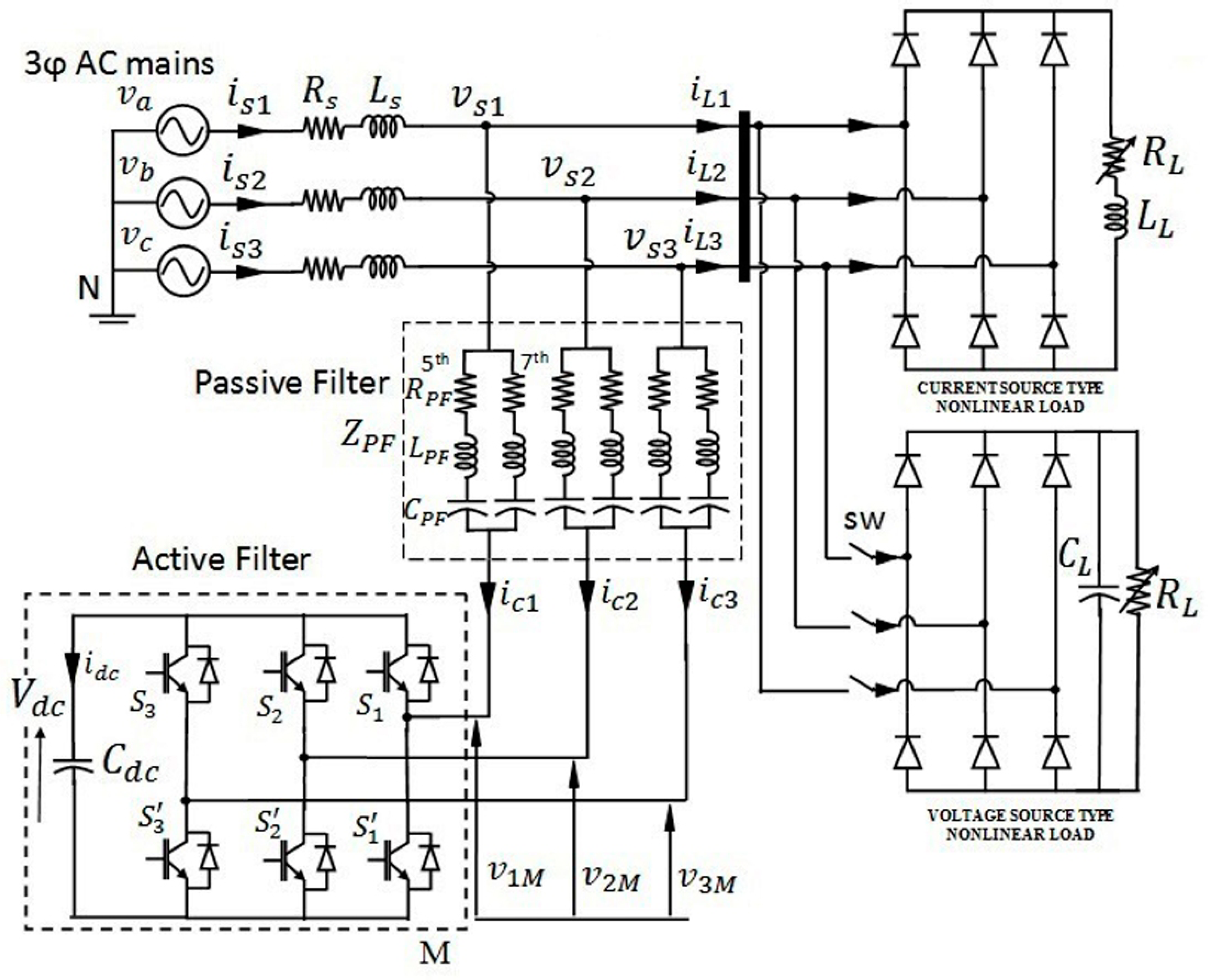
2. System Configuration of Hybrid Compensator

The system shown in Figure 1 consists of a standard three-phase 400 V, 50 Hz mains connected to a pair of three-phase uncontrolled bridge rectifiers feeding individual R-L, R-C loads, which introduce harmonic currents in the supply system due to the nonlinearity. The shunt compensator contains 5th and 7th tuned passive filters, which are in parallel and the combination is connected in series with low voltage rated active power filter. The parallel connected passive filters having selective harmonic elimination are meant for effective reactive power compensation. This system eliminates the inherent disadvantages of both active and passive filters. The hybrid compensator is operated such that the distortion currents generated due to nonlinear loads are confined within the PPF and do not flow in the AC supply mains. The fundamental voltage drop across passive power filter components permits shunt APF to operate at low DC link voltage. The three-phase source voltage, the voltage at the point of common coupling, load and compensator currents are denoted as Vabc, Vs123, iL123 and ic123, respectively, and shown individually in Figure 1.

2.1. Modelling of Shunt Hybrid Power Compensator

By applying Kirchhoff’s laws in Figure 1, the following equations in differential form in stationary three-phase reference frame are obtained, where the RPFe, LPFeq and CPFeq are equivalent parameter values of the 5th and 7th selective harmonic filters.
v s k = L P F e q d i c k d t + R P F e q i c k + ( 1 / C P F e q ) i c k d t + v k M + v M N
where k = 1, 2, 3 represent the three phases.
Differentiation of Equation (1) to eliminate the integral term yields
d v s k d t = L P F e q d 2 i c k d t 2 + R P F e q d i c k d t + 1 C P F e q i c k + d v k M d t + d v M N d t
Assuming balanced three-phase supply voltage yields
v s 1 + v s 2 + v s 3 = 0
Summing the three equations included in (1) for k = 1, 2, 3 and assuming nonexistence of the zero-sequence current into three-wire system [16] results in
v M N = 1 3 k = 1 3 v k M
The switching function C k   [12] of the kth leg of the inverter is the state of the power semiconductor devices   S k and   S k and is defined as
C k = { 1 ,   i f     S k     i s   O n     a n d     S k     i s   O f f 0 ,   i f   S k   i s   O f f   a n d   S k   i s   O n
Thus, with v k M = C k V d c and differentiation of the same, this leads to
d v k M d t = C k d V d c d t
By differentiating Equation (3), we get
d v M N d t = 1 3 k = 1 3 d d t ( C k V d c )
Substitution of Equations (5) and (6) into (2) and rearranging the same yields
d 2 i c k d t 2 = R P F e q L P F e q d i c k d t 1 C P F e q L P F e q i c k 1 L P F e q ( C k 1 3 m = 1 3 C m ) d V d c d t + 1 L P F e q d v s k d t
defining the switching state function as q n k = ( C k 1 3 m = 1 3 C m ) n , where, n = 0 or 1.
In other words, the vector q n epends on the parameters C 1 , C 2 , C 3 through a matrix transformation given below, indicating the interaction among the three phases [15].
[ q n 1 q n 2 q n 3 ] = 1 3 [ 2 1 1 1 2 1 1 1 2 ] [ C 1 C 2 C 3 ]
d 2 i c k d t 2 = R P F e q L P F e q d i c k d t 1 C P F e q L P F e q i c k 1 L P F e q q n k d V d c d t + 1 L P F e q d v s k d t
The capacitor current   i d c = i c 1 + i c 2 + i c 3 and is related to V d c by
d V d c d t = 1 C d c i d c
Expressing the DClink capacitor current i d c in terms of the switching and compensator currents, the following equation is obtained
d V d c d t = 1 C d c k = 1 3 q n k i c k = 1 C d c [ q n 123 ] T [ i c 123 ]
In the nonexistence of zero-sequence currents, the variables i c 3 and q n 3 can be eliminated by the substitution of i c 3 = ( i c 1 + i c 2 ) and q n 3 = ( q n 1 + q n 2 ) so that Equation (11) for the modelling of the capacitor is modified as follows.
d V d c d t = 1 C d c [ 2 q n 1 + q n 2 ] i c 1 + 1 C d c [ q n 1 + 2 q n 2 ] i c 2
The complete model of the shunt hybrid power compensator in abc reference frame is indicated by Equations (9) and (12).

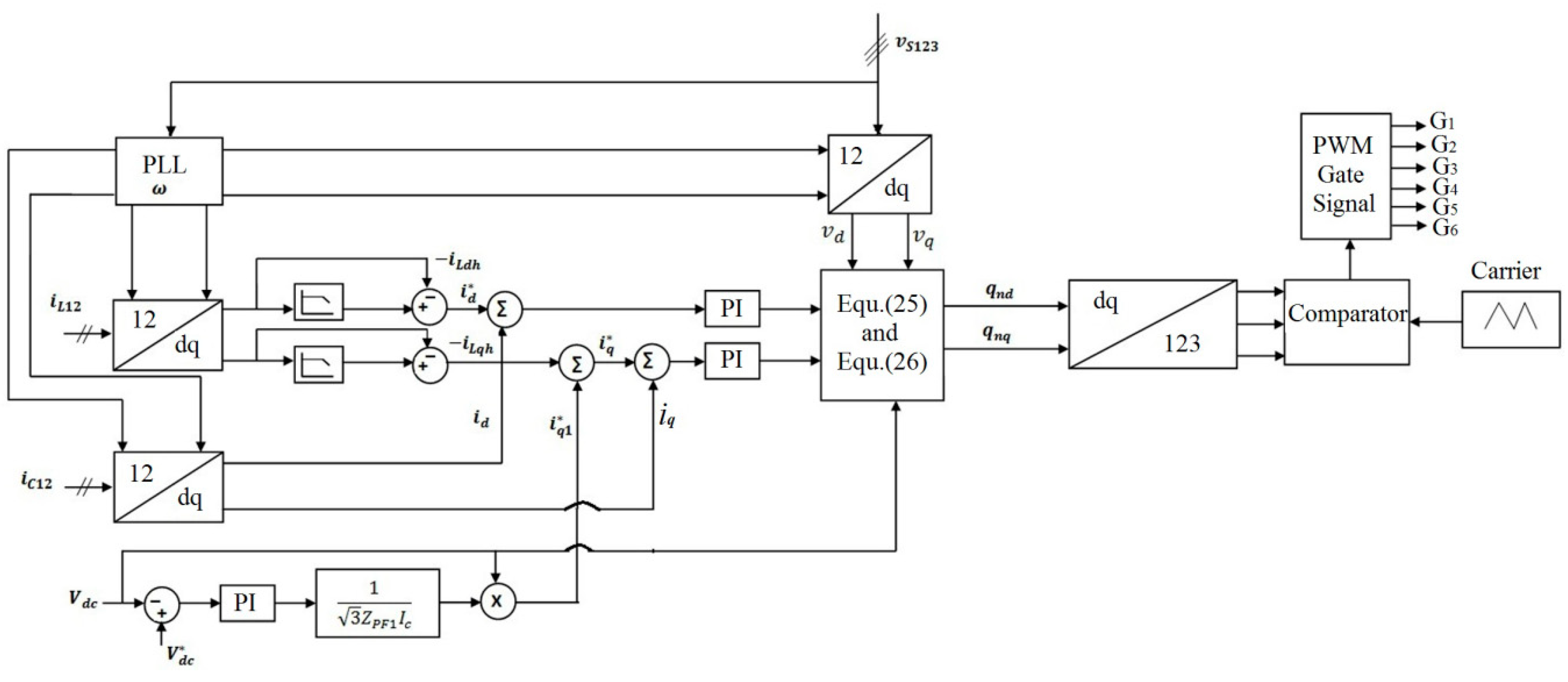
2.2. Equations in dq Frame

The model given by Equations (9) and (12) is transformed into synchronous orthogonal frame using the transformation matrix [13]
T d q 123 = 2 3 [ cos θ cos ( θ 2 π 3 ) cos ( θ 4 π 3 ) sin θ sin ( θ 2 π 3 ) sin ( θ 4 π 3 ) ]
where θ = ω t and ω represents the mains frequency.
Since T d q 123 is orthogonal, ( T d q 123 ) 1 = ( T d q 123 ) T and Equation (12) can be written as
d V d c d t = 1 C d c ( T d q 123 [ q n d q ] ) T ( T d q 123 [ i d q ] ) = 1 C d c [ q n d q ] [ i d q ]
On the other hand, Equation (9) can be written as
d 2 d t 2 [ i c 12 ] = R P F e q L P F e q d d t [ i c 12 ] 1 C P F e q L P F e q [ i c 12 ] 1 L P F e q [ q n 12 ] d V d c d t + 1 L P F e q d d t [ v s 12 ]
The three-phase current with the absence of zero-sequence components can be converted into d-q frame using reduced transformation matrix. Applying the transformations in Equation (15), the complete d-q frame dynamic model of the system is obtained as follows;
L P F e q d 2 i d d t 2 = R P F e q d i d d t + 2 ω L P F e q d i q d t ( ω 2 L P F e q + 1 C P F e q ) i d + ω R P F e q i q q n d d V d c d t + d v d d t ω v q
L P F e q d 2 i q d t 2 = R P F e q d i q d t 2 ω L P F e q d i d d t ( ω 2 L P F e q + 1 C P F e q ) i q ω R P F e q i d q n q d V d c d t + d v q d t + ω v d
C d c d V d c d t = q n d i d + q n q i q
The role of i d in Equation (16) is interpreted as the component for meeting the switching losses in the compensator, whereas the component i q is utilised to supply reactive power and maintain the DClink voltage across the capacitor for sustaining the compensator action.
It is specifically noted that this set of Equations (16)–(18) contain nonlinear terms involving the control variables q n d and q n q . Accordingly, the implementation of this control strategy is termed as nonlinear control technique by many authors in the literature [12,15,16].

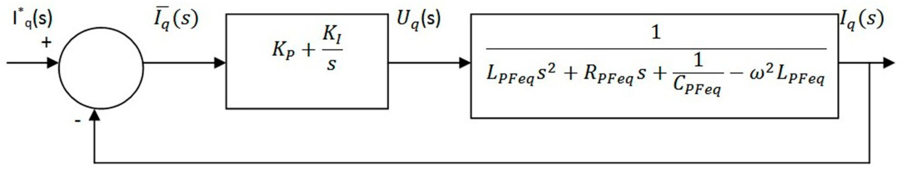
2.3. Control of Harmonic Currents

Based on the load and compensator models presented in Section 2.2, the control problem is formulated with the objective of minimizing supply-side current harmonics and improving the power factor. Also, for maintaining the performance during load fluctuations, it is necessary to maintain a desired DC link capacitor voltage. The control law is derived using the following approach.
Rewriting Equations (16) and (17) in a more convenient form, we get
L P F e q d 2 i d d t 2 + R P F e q d i d d t + ( ω 2 L P F e q + 1 C P F e q ) i d = 2 ω L P F e q d i q d t + ω R P F e q i q q n d d V d c d t + d v d d t ω v q
L P F e q d 2 i q d t 2 + R P F e q d i q d t + ( ω 2 L P F e q + 1 C P F e q ) i q = 2 ω L P F e q d i q d t ω R P F e q i d q n q d V d c d t + d v q d t + ω v d
The control variables u d and u q are defined as
u d = 2 ω L P F e q d i q d t + ω R P F e q i q q n d d V d c d t + d v d d t ω v q
u q = 2 ω L P F e q d i d d t ω R P F e q i d q n q d V d c d t + d V q d t + ω v d
Using the idea of decoupling the current harmonic components for the purpose of tracking the reference current, the error signals i ¯ d = i d i d and i ¯ q = i q i q   are generated and processed through a pair of PI controllers [12,14] to obtain u d and u q signals which are given below.
i d and   i q are the reference currents deduced from the load current, i d and i q are the actual compensator currents.Load current in d-q coordinate is processed using a pair of fourth-order Butterworth low-pass filters with cut-off frequency set at 60 Hz to extract the harmonic current references alone.
u d = K P i ¯ d + K I i ¯ d d t
u q = K P i ¯ q + K I i ¯ q d t
From Equations (19) and (20), we obtain the transfer function as follows
I d ( s ) U d ( s ) = I q ( s ) U q ( s ) = 1 L P F e q ( s 2 + R P F e q L P F e q s + 1 C P F e q L P F e q ω 2 )
The current control of the closed-loop system is shown in Figure 2 and represents the signal flow of the variables i q ( s ) ; the other component i d ( s ) is obtained concurrently in a similar manner. The transfer function of the full closed-loop control module is derived as
I q ( s ) I q ( s ) = K P L P F e q [ s + K I K P s 3 + R P F e q L P F e q s 2 + ( 1 C P F e q L P F e q ω 2 + K P L P F e q ) s + K I L P F e q ]
From Equations (21) and (22), the control variables of the proposed system are defined by the following equations.
q n d = 2 ω L P F e q d i q d t + ω R P F e q i q + d V d d t ω v q u d d V d c d t
q n q = 2 ω L P F e q d i d d t + ω R P F e q i d + d V q d t ω v d u q d V d c d t
The above equations represent both the decoupled linear compensation part and cancellation of nonlinearity.

2.4. DC Link Voltage Control

The capacitor in the APF does not need any external DC source but gets charged through the rectifier action of the built-in reverse diodes across the six Insulated-gate bipolar transistors (IGBTs). The power loss in the capacitor and switching losses in the inverter have to be met by the active component id of the compensator current from the mains, while the component iq supplies the reactive power stored in the capacitor. The power losses in this circuit can reduce the DC link capacitor voltage, thereby weakening the function of the active filter. Hence, it is necessary to maintain the voltage across the DC link capacitor at a designed reference value by an additional voltage regulator, which modifies the PWM signals appropriately. This regulator is implemented by using a PI controller [12], which processes the error between the reference voltage V d c and the actual capacitor voltage Vdc. The parameters of the PI regulator are chosen in such a way that the DC voltage is maintained around its desired value. The design values for the PI controller parameters have been obtained following the approach suggested by Salem Rahmani et al. [13,14]. The overall transfer function of this controller is incorporated as a subsystem in the simulation schematic.
The control scheme of the proposed hybrid power compensator is shown in Figure 3, where the various signals such as Vdc, V d c , i d , i q , i d and i q are processed using Equations (21) to (26) to obtain the gate trigger signals.

2.5. Simulink Model of the Shunt Hybrid Power Compensator

The Simulink schematic of the power distribution system along with the proposed shunt hybrid power compensator, which translates the entire system equations presented in Section 2 into functional blocks in the Simulink model, has been developed using MATLAB software. The nonlinear load has been modelled using a three-phase full bridge diode rectifier feeding RL and RC loads separately as subsystems and connected to the three phase mains. At the source side, a resistor–inductor combination is used to represent the line impedance of each phase before PCC. The unbalance case in the nonlinear load has been formed by connecting a single-phase diode rectifier feeding RL load between phase1 and ground. The synchronization of the subsystem with main supply frequency is accomplished by using a three-phase discrete PLL block [22,23,24,25]. The PLL block detects the supply frequency; the detected supply frequency is used to synchronize the compensator d-q axis current and the distorted load d-q axis current to extract harmonic component needs to be compensated. During load disturbance and supply voltage distortions, the variation in the supply frequency is detected by the PLL block and synchronizes the subsystems accordingly.
The hybrid filter consists of a parallel connection of selective 5th and 7th harmonic elimination passive filters as depicted in Figure 1 along with APF. The entire system simulation is carried out in a discrete mode, variable step size with ode45 (Dormand–Prince) solver.

3. Simulation Results

To evaluate the performance of the shunt HPF controlled by the proposed control algorithm, a Simulink-based schematic was created so as to operate from a 400 V, 50 Hz supply. The load consists of a set of balanced and unbalanced nonlinear loads, which are selectively connected for successive simulation runs. In this work, the performances of the compensator corresponding to the following loads are analysed: (i) three-phase rectifier feeding RL load, (ii) three-phase rectifier feeding RC load, (iii) dynamic load variation and (iv) unbalanced load. Table 1 indicates the specification of the system parameters used in the simulation.

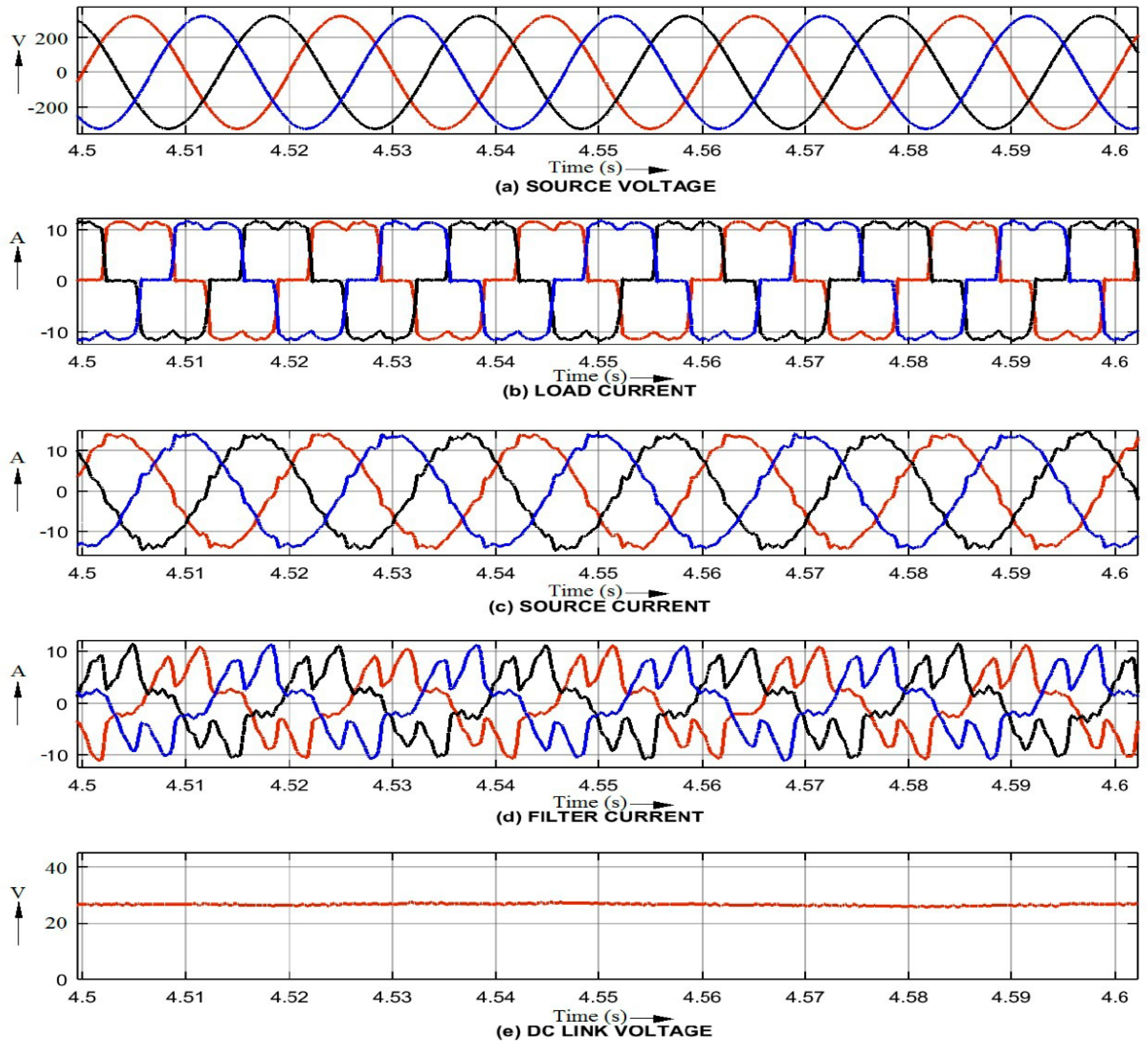
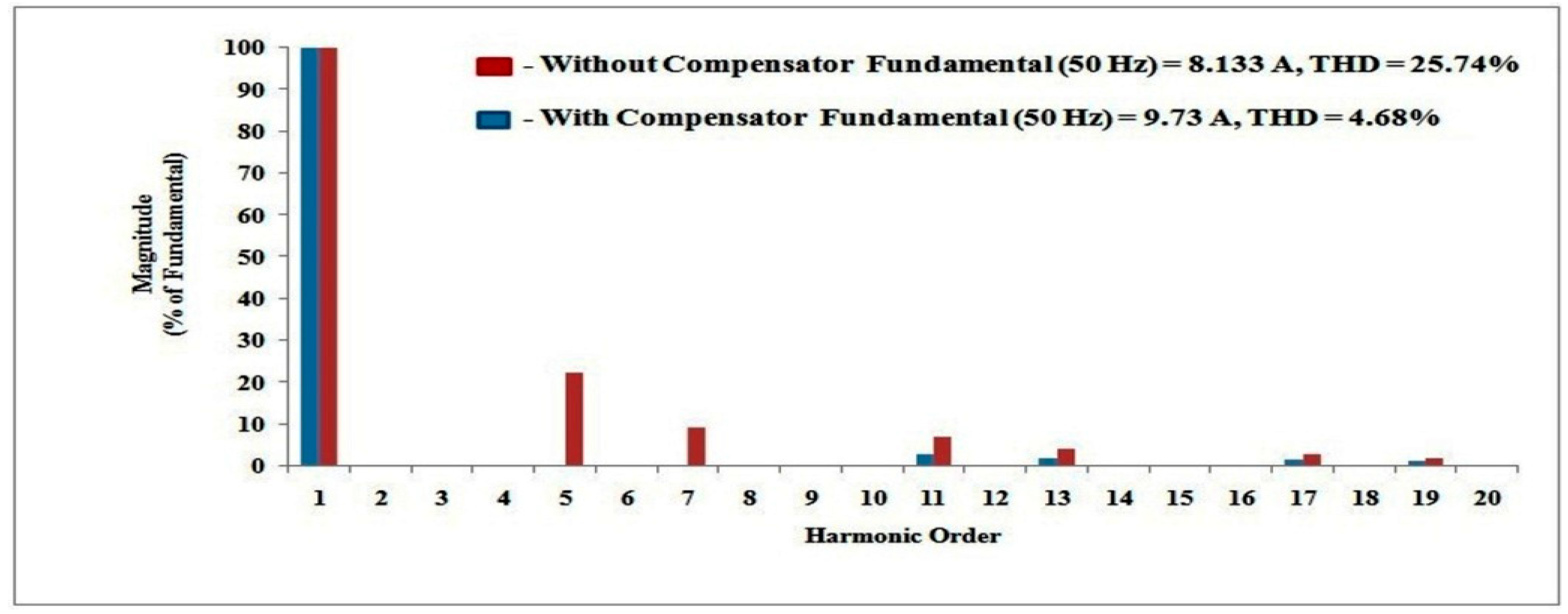
3.1. Performance of Shunt HPF to the Nonlinear Load of Current Source Type

The three-phase mains supply a diode bridge rectifier, whose output is wired to a balanced R-L load, which imposes a typical nonlinearity, resulting in harmonic currents at the supply end. The proposed hybrid shunt compensator is wired at PCC as shown in Figure 1. The results are shown in Figure 4a–e covering the waveforms of the supply voltage, currents of the load, source current after compensation, currents of the compensator and DC link voltage, respectively. The waveform depicts that the supply current waveform is almost sinusoidal after compensation and the DC link capacitor voltage is maintained constant. Figure 5 depicts the simulation results covering the harmonic spectrum of the supply current before and after compensation. The results indicate that the THD of the supply current is reduced from 25.74% without compensator to 4.68% with compensator. It is seen that the proposed control strategy with shunt HPF can mitigate the current harmonics present in the supply system within the limit specified by IEEE 519-1992 standards.

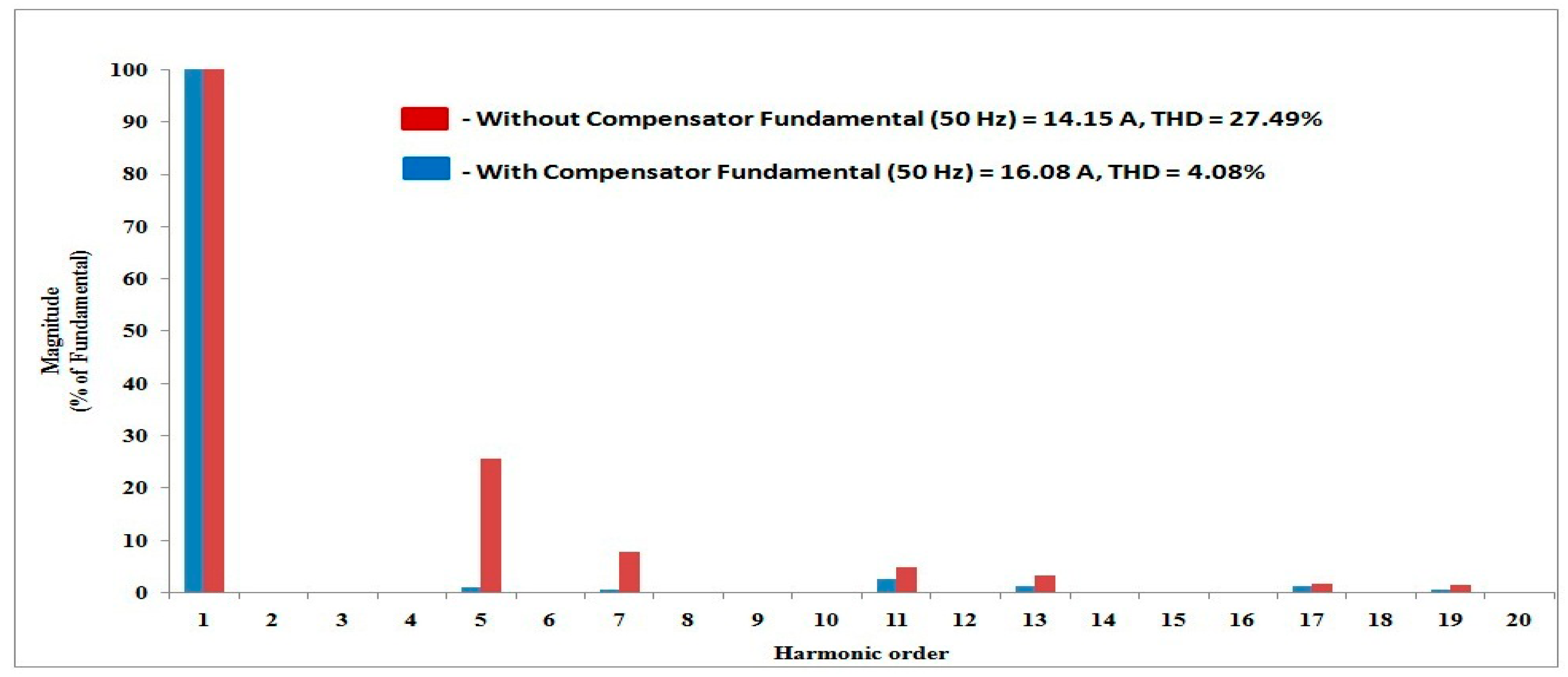
3.2. Varying Three-Phase Rectifier-Fed RL Load

Since the load in a distribution system can vary concerning time, it is essential to verify the suitability of the designed filter under varying load conditions. The simulation results for sudden change of load current from 9.74 A (rms) to 17.17 A at t = 4 s and restoration of the same to the previous value at t = 4.1 s are presented in Figure 6a–e covering source voltage, load current, source current, compensator current and DC link voltage waveforms, respectively. The THD of the supply current before step change in the load current has been improved from 25.74% without compensator to 4.55% with compensator. Similarly, after a step change in the load current, the supply current THD has been reduced from 23.06% to 4.14% with compensator. In both the cases, the compensator is capable of maintaining the THD of the source-side current within the limit specified by the IEEE 519-1992 standards. It is observed from Figure 6e,c that the compensator is able to maintain the DC link voltage as constant and supply current waveforms to be sinusoidal.

3.3. Three-Phase Rectifier-Fed RC Load

The load in the simulation schematic is replaced by an R-C circuit with parameter values as shown in Table 1 and the simulation is executed to obtain the performance of the compensator. Figure 7a–e shows the source voltage, load current, supply current after compensation, compensator current and DC link voltage waveforms, respectively. It is observed from the figures that the DC link voltage of the compensator is maintained constant during compensation, and the supply current variation approaches a sinusoidal waveform. Figure 8 shows the harmonic spectrum of line currents from mains before and after compensation. It shows that the THD of the source current is reduced considerably from 27.49% to 4.08%. The system is highly nonlinear and subjected to disturbances due to loading. Hence, in practice, the DC link voltage varies slightly due to ripples and disturbances inherent in the operation of the compensator.

3.4. Varying Three-Phase Rectifier-Fed RC Load

By introducing a 100% step increase followed by a similar decrease in the load current of the R-C circuit, the ability of the hybrid compensator to mitigate the harmonic current under varying load conditions is examined in the simulation setup. The results of this simulation, where the load current changes from 16.05 A (rms) to 30.32 A at t = 2 s and restoration of the same to 16.05 A are shown in Figure 9a–e. These depict the supply voltage, load current, supply current after compensation, compensator current and the DC link voltage, respectively. The obtained results indicate that the desirable features in the performance of the hybrid filter are maintained even after the step changes in the load within a very short time. The THD of the source current has been reduced from 27.49% without compensator to 3.46% with compensator before the step change is made in the load current. Similarly, the THD has been reduced from 20.91% to 4.77% after the step change. It is seen that the compensator operation reduces the harmonic content within a THD of 5%, in addition to maintaining a steady DC link voltage.

3.5. Unbalanced Loading Condition

To study the performance of a shunt hybrid power compensator employing synchronous rotating reference-based nonlinear control method, an unbalance in load is created by connecting a single-phase rectifier feeding R-L load across the phase ‘a’ and phase ‘b’ of the supply system. The compensation performance at steady state of the proposed compensator, such as the supply voltage, load current, supply current, compensator current and DC link voltage waveforms, is depicted in Figure 10a–e. The THD of supply phase ‘a’ current is reduced from 9.46% to 2.54% after compensation. Similarly, supply phase ‘b’ current has been reduced from 7.04% to 1.91%, while phase ‘c’ current has been reduced from 25.47% to 5.37%.
It is seen from the obtained results that the proposed control method with shunt hybrid compensator effectively compensates the harmonic distortion present in the supply current under unbalanced loading conditions.
Since the load in a distribution system can vary with respect to time, it is essential to verify the suitability of the designed filter under varying load conditions. During dynamic variations in the load current and unbalance, as shown in Figure 6, Figure 9 and Figure 10, the compensator is able to maintain constant DC link voltage as well as reduce the amount of harmonics present in the system.

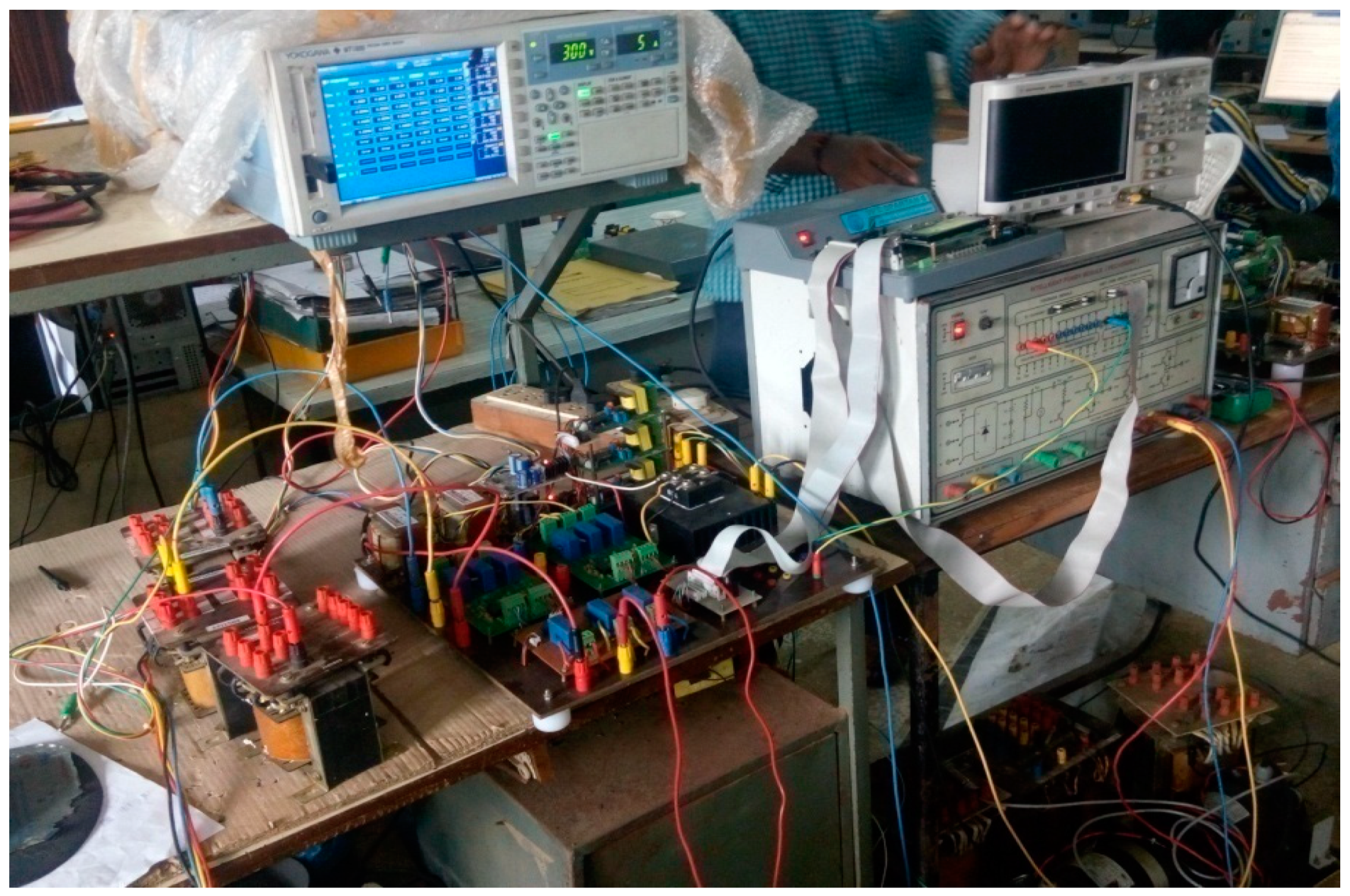
4. Hardware Fabrication

A prototype of the distribution system along with the passive and active parts of the hybrid compensator has been fabricated and experimental work on the same was carried out. Figure 11 shows the overall setup of the experimental work. The active filter part of the prototype has been developed using intelligent power module PEC16DSMO1. The IPM consists of a three-phase six-pulse inverter with six IGBT semiconductor power switches and is controlled in real time based on the software control program from the SPARTAN-6 FPGA development board. These IGBT switches are capable of operating at high frequencies of the carrier waveform up to 20 kHz.

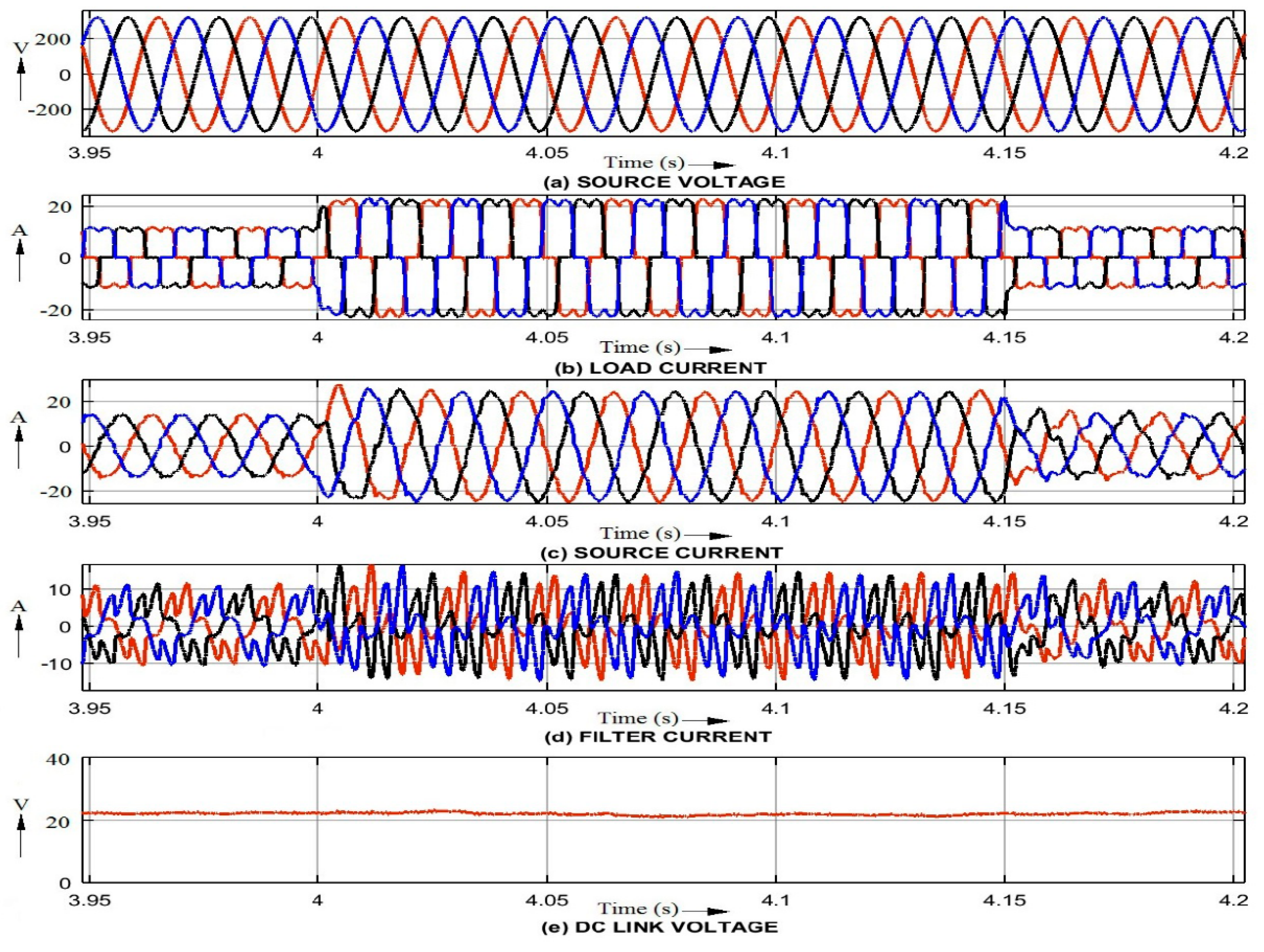
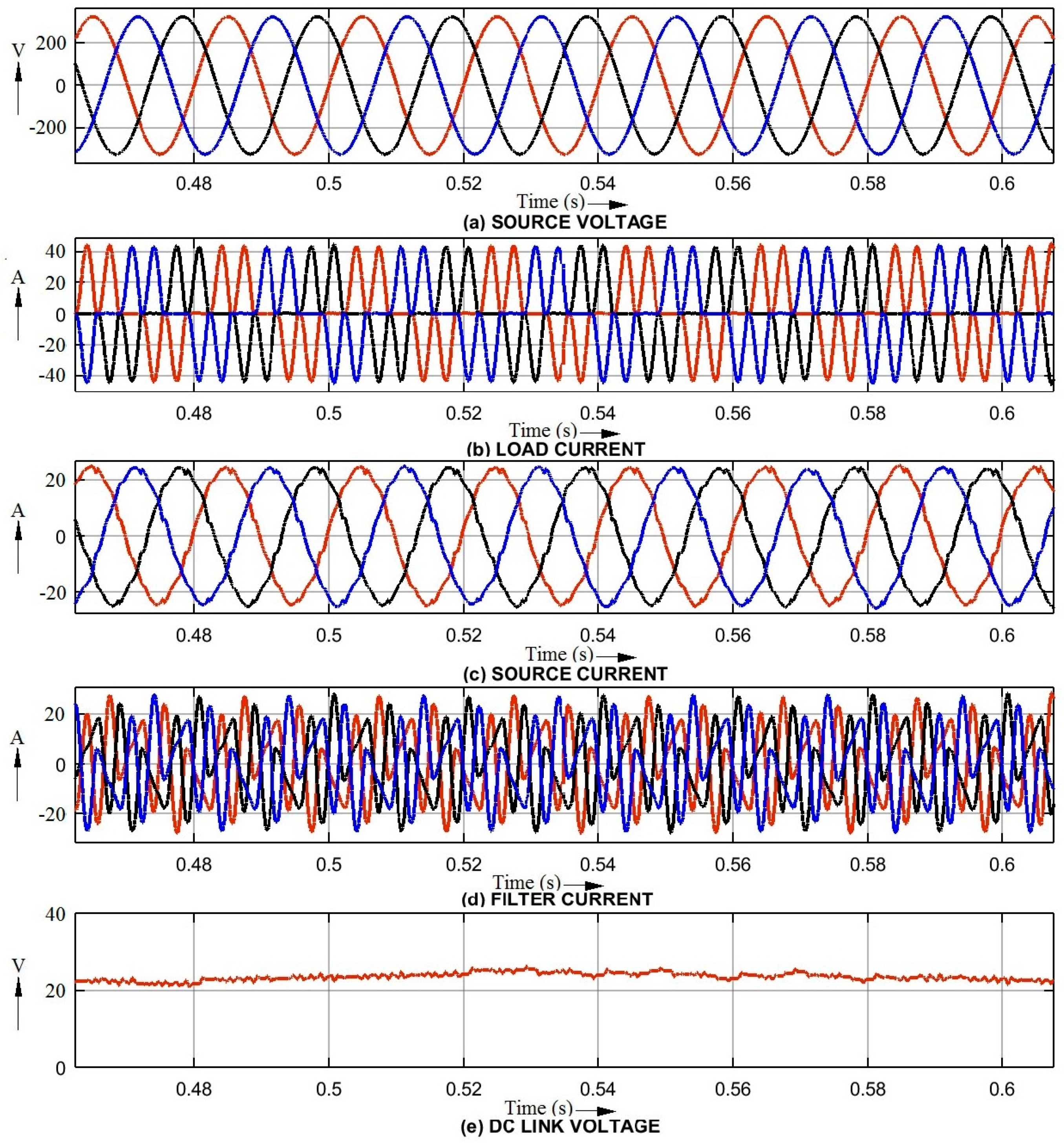
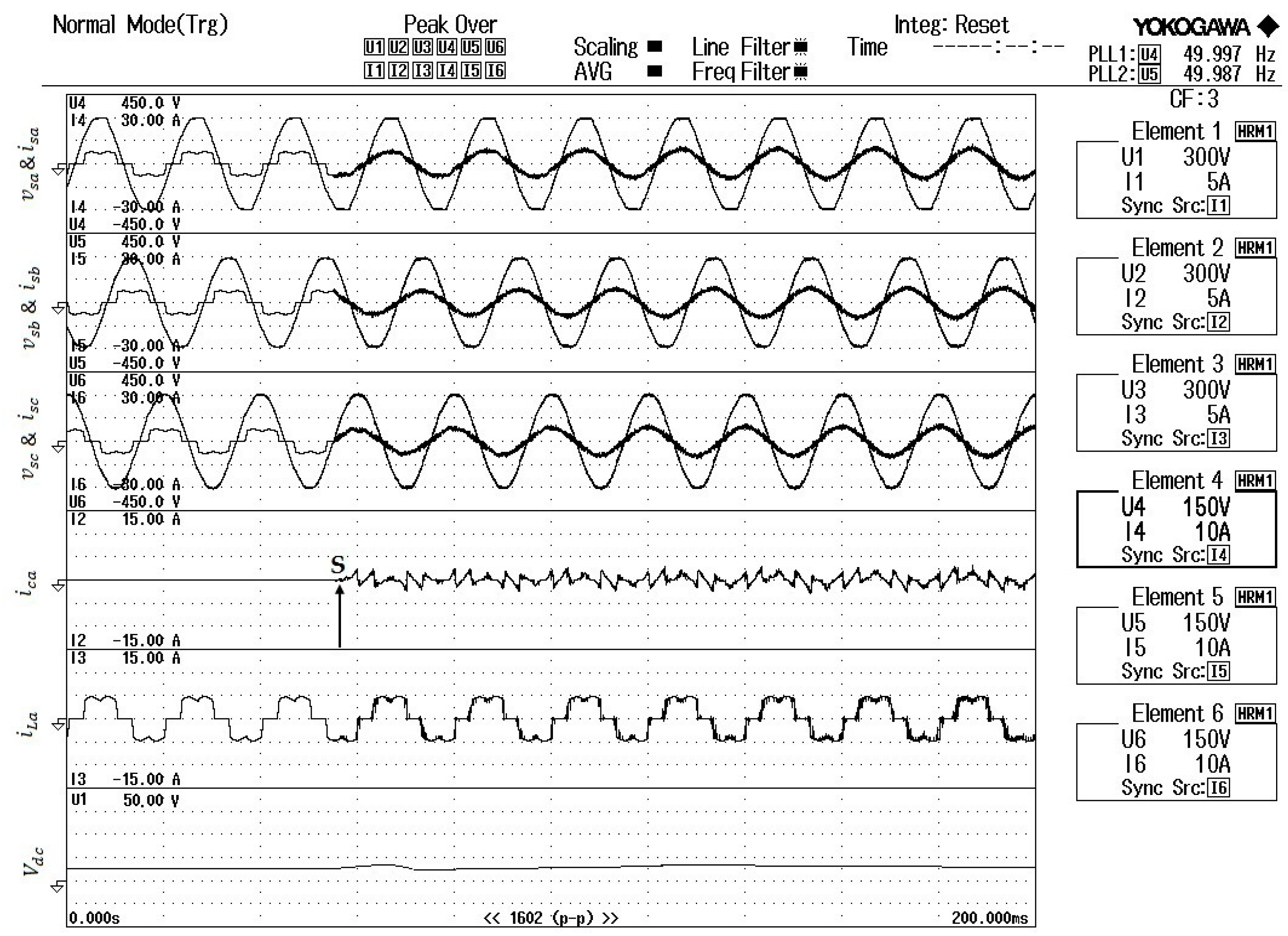
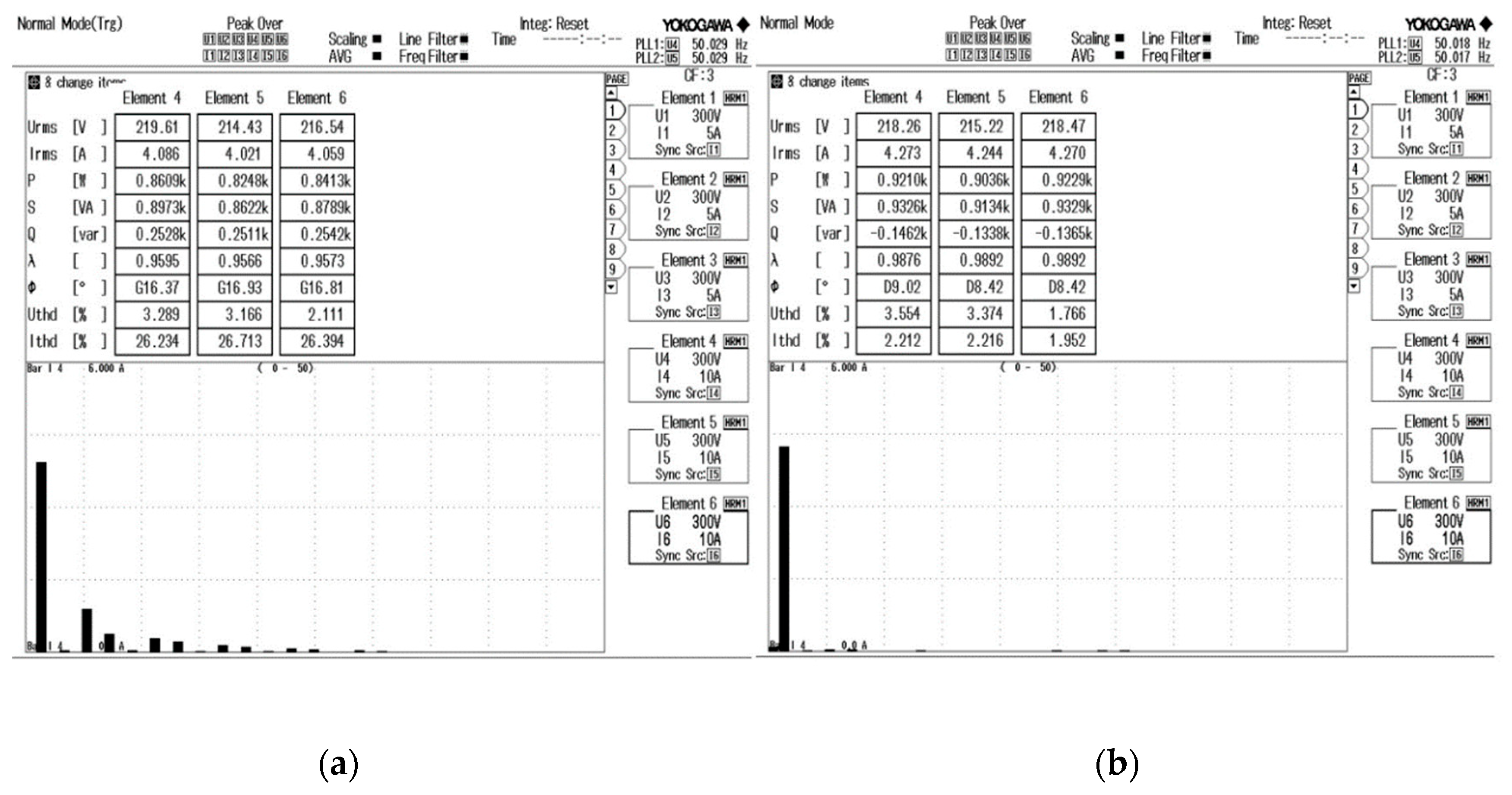
4.1. Hardware Resultsand Discussion

A series of experiments involving different types of loads and their dynamic variations have been conducted, and the performance of the compensator has been evaluated. A six-channel YOKOGAWA Power Quality Analyser has been used to capture the signals such as supply voltage, source current, load current, compensator current and DC link voltage. The hardware system parameters are shown in Table 2

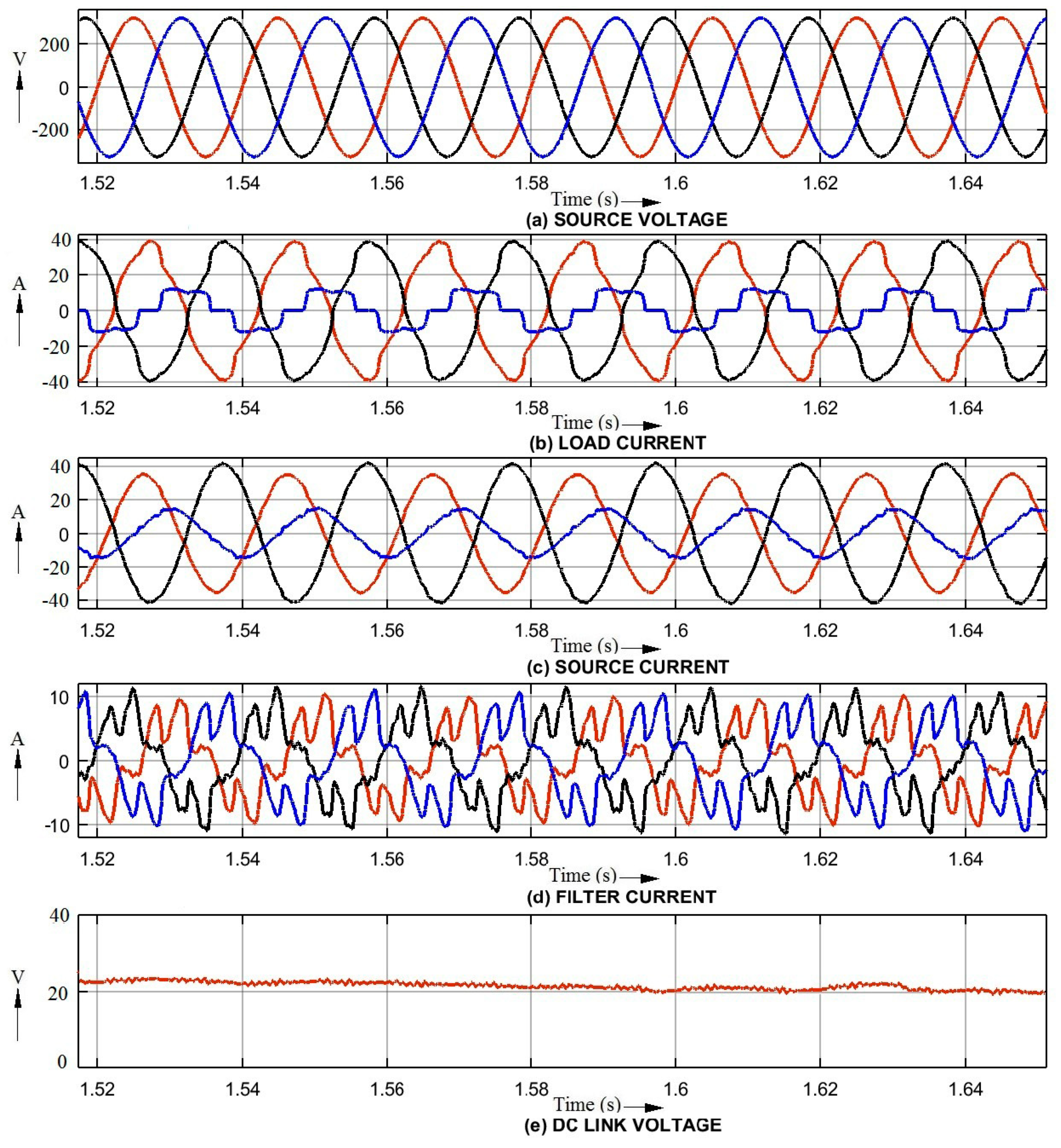
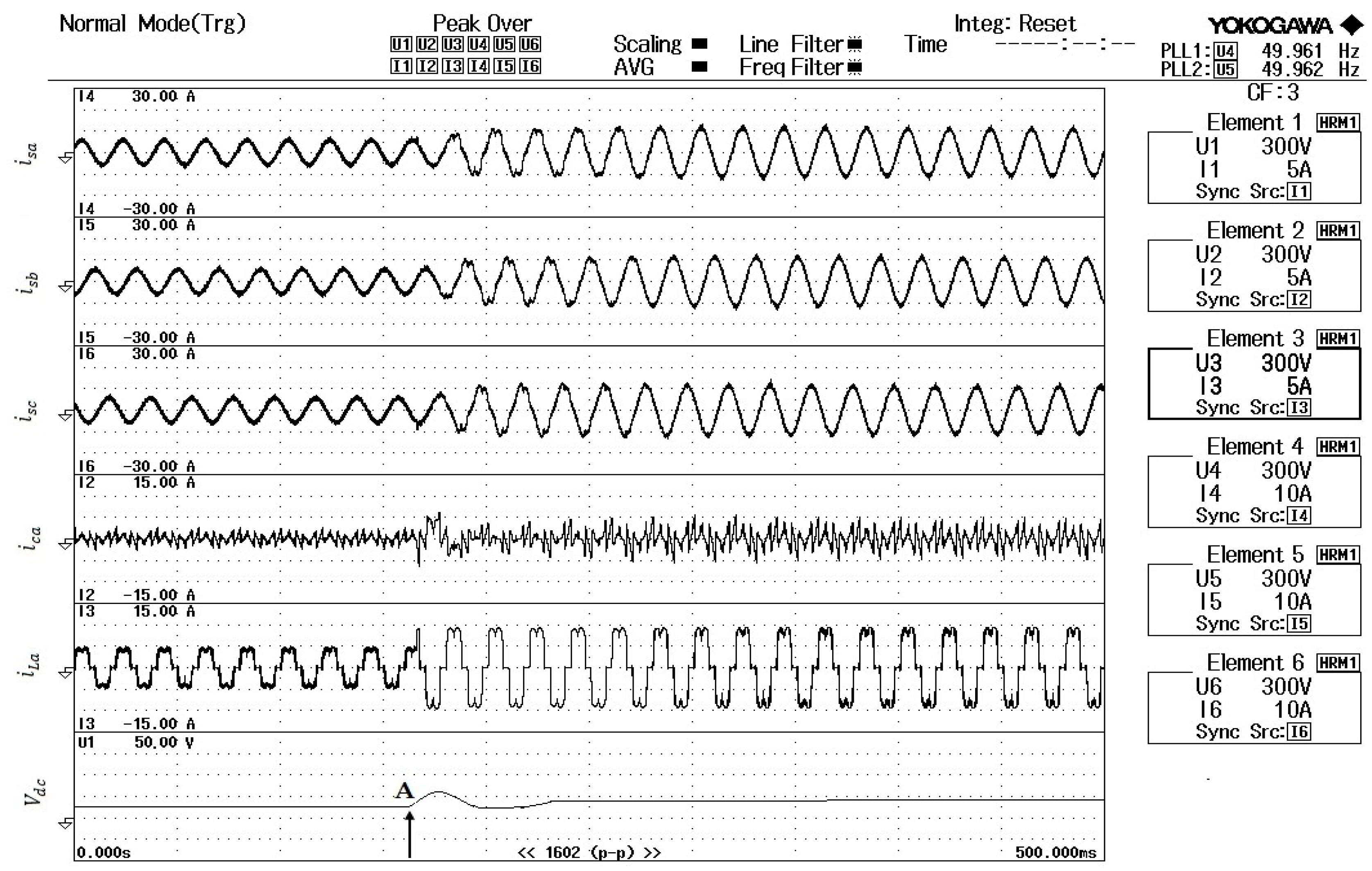
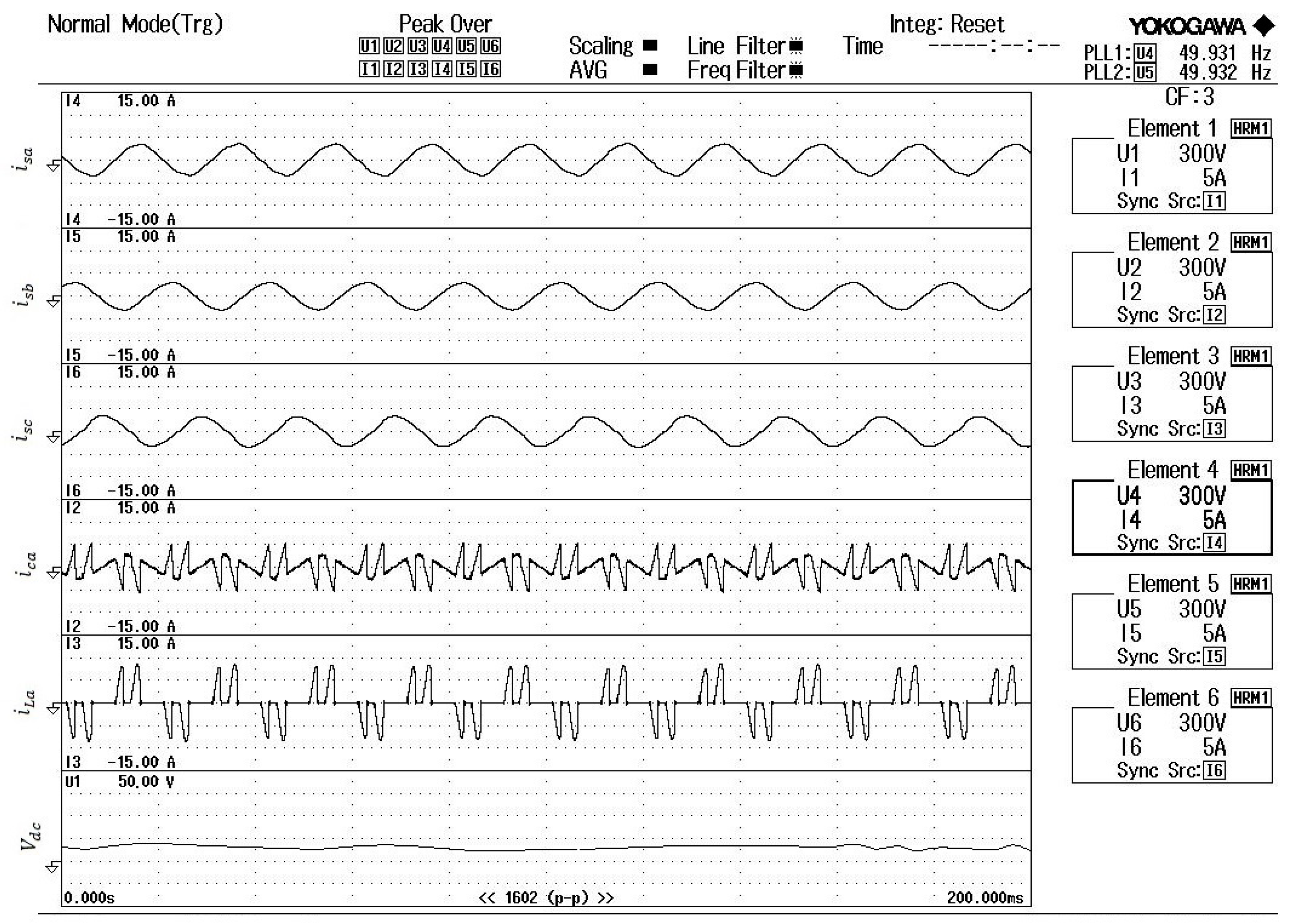
4.1.1. Performance of the Compensator for Current Source Type Nonlinear Load

Figure 12 shows the experimental response of the compensator for the current source type nonlinear load. The compensation performance of the hybrid filter has been verified by turn on the compensator at the point ‘S’ as shown in Figure 12. It is seen from the figure that the source current becomes sinusoidal after the operation of compensator at point ‘S’. The harmonic spectrum of the source current without and with compensator is shown in Figure 13a,b and it is observed that the THD of the source current has been reduced from 26.225% to 2.212%.

4.1.2. Performance of the Compensator for Varying Current Source Type Nonlinear Load

The performance of the hybrid compensator has been verified experimentally by creating a step change in the load current at ‘A’ as shown in Figure 14. It is observed that the source current in all the three phases are sinusoidal and the compensator is able compensate the harmonic distortion even after a step change in the load current. The THD of the source current after compensation has been observed as 3.26%, which is less than 5% as specified by IEEE 519-1992 standards.

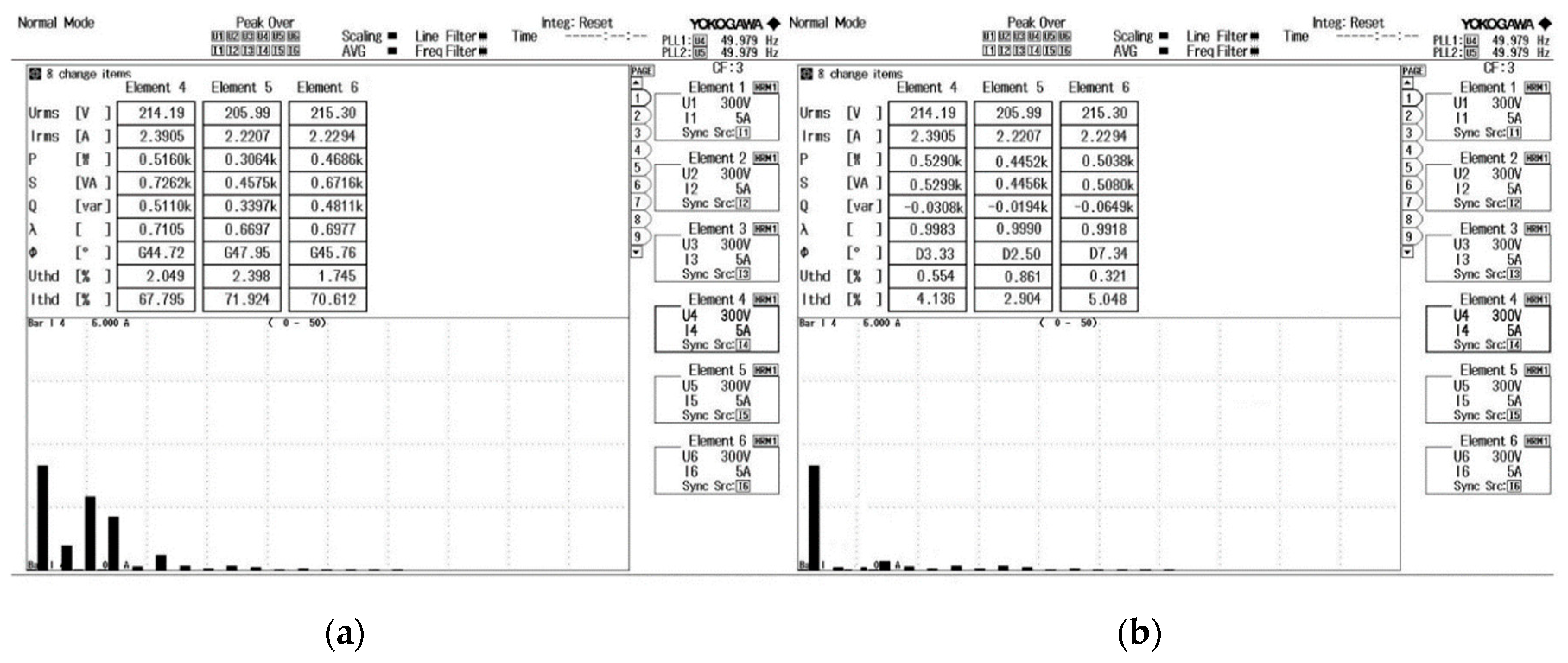
4.1.3. Performance of the Compensator for Voltage Source Type Nonlinear Load

The performance of the compensator for voltage source type nonlinear load has been experimentally verified by connecting the nonlinear load in the three-phase supply system. Figure 15 shows the three-phase source currents of all phases individually, compensator current of one phase, load current of one phase and DC link voltage, respectively. It is seen that the supply current after compensation is sinusoidal without distortion and the DC link voltage of the compensator is also maintained constant.
The FFT spectrum of the source current before and after compensation is shown in Figure 16a,b, respectively. It is observed from the FFT spectrum that the supply current harmonics have been reduced from 67.795% without compensator to 4.136% with compensator. It has been confirmed from the above results that the designed control strategy with proposed shunt hybrid power compensator is able to effectively compensate both the types of nonlinear load distortions present in the supply current. It is observed that the experimental work results are closely matching with simulation work results in all cases and the obtained performance waveforms are also matching with each other.

4.1.4. Performance Comparison and Discussion

Performance of the proposed hybrid filter with the adopted control strategy has been compared with some other control methods proposed in the literature. Table 3 shows the comparison of various control techniques proposed in the literature for harmonic reduction. It is clearly understood from Table 3 that the synchronous rotating reference theory based nonlinear control with the adopted hybrid filter topology proposed in this work gives better THD in the source current during supply feeds of different types of nonlinear loads. Most of the techniques proposed in the literature cover only current source type nonlinear load. In this work, different types of nonlinear loads and various loading conditio..ns are considered during simulation and experimental work. The experimental work has been carried out for low current rating nonlinear loads compared to the simulation work. Hence, it has been observed that the experimental THD values are better than the simulation results. Furthermore, the hardware setup has been developed for low rating loads only due to the cost. The results of simulation indicate effectiveness of the compensator topology and versatility of the control scheme for meeting the requirements of a set of nonlinear loads indicated above. In addition, the kVA ratings of the designed active filter for both types of load are only a small percentage of the respective load ratings, which is a major advantage of this scheme. Although the overall performance of the hybrid compensator has been highly satisfactory, while covering alternate cases of load, their fluctuations and unbalance, it appears that the PI controller-based algorithm shows a minor deficiency, when the passive filter parameter values undergo even minor changes. This can be traced to the presence of fixed values of the PI controller gain and time constant parameters. A possible and feasible solution to this issue of filter parameter variations is to adaptively adjust the PI parameters’ value. Although a three-phase distribution system for power quality enhancement has been considered in this paper, it is limited to a three-wire system only with isolated neutral. Hence, issues arising out of zero-sequence currents due to load unbalance have not been considered. This research work can be extended for a three-phase, four-wire system. Further, incorporation of controllers utilizing various other soft computing techniques like neural, fuzzy-neural and genetic algorithms can be carried out as further work.

5. Conclusions

A three-phase hybrid compensator scheme discussed in this paper is configured with 5th and 7th selective harmonic elimination passive filter in series with an active filter in the form of an IGBT-based PWM inverter, triggered using a control algorithm, based on a synchronously rotating reference frame (SRRF) in the d-q axis. The overall objective is to improve the steady state power factor and to ensure dynamic harmonic compensation at the supply side of three-phase mains. Accordingly, the entire system is simulated using Simulink and the results are presented, covering a set of nonlinear loads. The simulation results indicate the effectiveness of the compensator topology and versatility of the control scheme for meeting the requirements of a set of nonlinear loads. It is seen that significant reduction of source current THD is obtained within limits specified by IEEE 519-1992 standard along with excellent regulation of the DC link voltage.
A series of experiments were carried out using the above prototype along with alternate nonlinear loads and the overall performance of the hybrid filter was recorded using six channels DSO. The THD values as measured by the DSO over a series of experiments were found to be closely matching with corresponding THD values obtained during simulation for all loading conditions. It is further verified that the experimental results compared favourably with the simulation waveforms, thereby validating the simulation model. The experimental results confirm the effectiveness of the SRRF-based control strategy for the hybrid compensator scheme to achieve source side current harmonics reduction and power factor improvement to near unity.

Author Contributions

Conceptualization, R.B. and K.P.; methodology, R.B. and K.P.; software, R.B. and K.P.; validation, R.B., K.P.; and R.S.; formal analysis, R.B.; investigation, R.B. and K.P.; data curation, R.B., and K.P.; writing—original draft preparation, R.B., K.P., R.S. and R.A.; writing—review and editing, R.S. and R.A.; supervision, R.S. and R.A.

Funding

This research received no external funding.

Acknowledgments

Authors wish to express their sincere thanks to acknowledge SASTRA Deemed University, Thanjavur, India 613401 for extending infrastructural support to carry out this work.

Conflicts of Interest

The authors declare no conflict of interest.

References

  1. Peng, F.Z. Harmonic sources and filtering approaches. IEEE Ind. Appl. Mag. 2001, 7, 18–25. [Google Scholar] [CrossRef]
  2. Dugan, R.C.; Mark, F.M.; Surya, S.; Wayne, H.B. Electrical Power Systems Quality, 3rd ed.; Tata McGraw-Hill Education: Noida, India, 2012; ISBN 9780071761550. [Google Scholar]
  3. Singh, B.; Singh, B.N.; Chandra, A.; Al-Haddad, K.; Pandey, A.; Kothari, D.P. A review of three-phase improved power quality AC-DC converters. IEEE Trans. Ind. Electron. 2004, 51, 641–660. [Google Scholar] [CrossRef]
  4. Wagner, V.E.; Balda, J.C.; Griffith, D.C.; McEachern, A.; Barnes, T.M.; Hartmann, D.P.; Phileggi, D.J.; Emannuel, A.E.; Horton, W.F.; Reid, W.E.; et al. Effects of harmonics on equipment. IEEE Trans. Power Deliv. 1993, 8, 672–680. [Google Scholar] [CrossRef]
  5. Das, J.C. Passive filters-potentialities and limitations. IEEE Trans. Ind. Appl. 2004, 40, 232–241. [Google Scholar] [CrossRef]
  6. Singh, B.; Al-Haddad, K.; Chandra, A. A review of active filters for power quality improvement. IEEE Trans. Ind. Electron. 1999, 46, 960–971. [Google Scholar] [CrossRef] [Green Version]
  7. Akagi, H. New trends in active filters for power conditioning. IEEE Trans. Ind. Appl. 1996, 32, 1312–1322. [Google Scholar] [CrossRef] [Green Version]
  8. Lam, C.-S.; Wong, M.-C. Design and Control of Hybrid Active Power Filters; Springer: Berlin, Germany, 2014. [Google Scholar]
  9. Singh, B.; Verma, V.; Chandra, A.; Al-Haddad, K. Hybrid filters for power quality improvement. IEE Proc.-Gener. Transm. Distrib. 2005, 152, 365–378. [Google Scholar] [CrossRef]
  10. Rivas, D.; Morán, L.; Dixon, J.W.; Espinoza, J.R. Improving passive filter compensation performance with active techniques. IEEE Trans. Ind. Electron. 2003, 50, 161–170. [Google Scholar] [CrossRef]
  11. Samadaei, E.; Lesan, S.; Cherati, S.M. A new schematic for hybrid active power filter controller. In Proceedings of the 2011 IEEE Applied Power Electronics Colloquium (IAPEC), Johor Bahru, Malaysia, 18–19 April 2011; pp. 143–148. [Google Scholar]
  12. Mendalek, N.; Al-Haddad, K.; Fnaiech, F.; Dessaint, L.A. Nonlinear control technique to enhance dynamic performance of a shunt active power filter. IEE Proc.-Electr. Power Appl. 2003, 150, 373–379. [Google Scholar] [CrossRef]
  13. Rahmani, S.; Hamadi, A.; Mendalek, N.; Al-Haddad, K. A new control technique for three-phase shunt hybrid power filter. IEEE Trans. Ind. Electron. 2009, 56, 2904–2915. [Google Scholar] [CrossRef]
  14. Rahmani, S.; Mendalek, N.; Al-Haddad, K. Experimental design of a nonlinear control technique for three-phase shunt active power filter. IEEE Trans. Ind. Electron. 2010, 57, 3364–3375. [Google Scholar] [CrossRef]
  15. Zouidi, A.; Fnaiech, F.; Al-Haddad, K. Voltage source inverter based three-phase shunt active power filter: Topology, Modeling and control strategies. In Proceedings of the 2006 IEEE International Symposium on Industrial Electronics, Montreal, QC, Canada, 9–13 July 2006; Volume 2, pp. 785–790. [Google Scholar]
  16. Mendalek, N.; Al-Haddad, K. Modeling and nonlinear control of shunt active power filter in the synchronous reference frame. In Proceedings of the Ninth International Conference on Harmonics and Quality of Power. Proceedings (Cat. No.00EX441), Orlando, FL, USA, 1–4 October 2000; Volume 1, pp. 30–35. [Google Scholar]
  17. Balasubramanian, R.; Sankaran, R.; Palani, S. Simulation and performance evaluation of shunt hybrid power filter using fuzzy logic based non-linear control for power quality improvement. Sadhana 2017, 42, 1443–1452. [Google Scholar] [CrossRef]
  18. Palandöken, M.; Aksoy, M.; Tümay, M. Application of fuzzy logic controller to active power filters. Electr. Eng. 2004, 86, 191–198. [Google Scholar] [CrossRef]
  19. Dey, P.; Mekhilef, S. Current controllers of active power filter for power quality improvement: A technical analysis. Automatika 2015, 56, 42–54. [Google Scholar] [CrossRef]
  20. Unnikrishnan, A.K.; Subhash Joshi, T.G.; Manju, A.S.; Joseph, A. Shunt hybrid active power filter for harmonic mitigation: A practical design approach. Sadhana 2015, 40, 1257–1272. [Google Scholar]
  21. Chauhan, S.K.; Shah, M.C.; Tiwari, R.R.; Tekwani, P.N. Analysis, design and digital implementation of a shunt active power filter with different schemes of reference current generation. IET Power Electron. 2013, 7, 627–639. [Google Scholar] [CrossRef]
  22. Cataliotti, A.; Cosentino, V. A Time-domain strategy for the measurement of IEEE standard 1459–2000 Power quantities in Non sinusoidal Three–phase and Single–phase systems. IEEE Trans. Power Deliv. 2008, 23, 2113–2123. [Google Scholar] [CrossRef]
  23. Cataliotti, A.; Cosentino, V. Disturbing Load Identification in Power Systems: A Single-Point Time–Domain Method Based on IEEE 1459–2000. IEEE Trans. Instrum. Meas. 2009, 58, 1436–1445. [Google Scholar] [CrossRef]
  24. Golestan, S.; Gurrero, J.M.; Vasquez, J.C. Three–Phase PLLs: A Review of Recent Advances. IEEE Trans. Power Electron. 2017, 32, 1894–1907. [Google Scholar] [CrossRef]
  25. Golestan, S.; Ge, J.M.; Vasquez, J.; Abusorrah, A.M.; Al-Turki, Y.A. Modeling, Tuning, and Performance Comparison of Second–Order-Generalized-Integrator–Based FLLs. IEEE Trans. Power Electron. 2018, 33, 10229–10239. [Google Scholar] [CrossRef]
  26. Balasubramanian, R.; Palani, S. Simulation and performance evaluation of shunt hybrid power filter for power quality improvement using PQ theory. Int. J. Electr. Comput. Eng. 2016, 6, 2603–2609. [Google Scholar] [CrossRef]
  27. Dey, P.; Mekhilef, S. Synchronous reference frame based control technique for shunt hybrid active power filter under non-ideal voltage. In Proceedings of the 2014 IEEE Innovative Smart Grid Technologies-Asia (ISGT ASIA), Kuala Lumpur, Malaysia, 20–23 May 2014; pp. 481–486. [Google Scholar]
  28. Bhattacharya, A.; Chakraborty, C.; Bhattacharya, S. Parallel-connected shunt hybrid active power filters operating at different switching frequencies for improved performance. IEEE Trans. Ind. Electron. 2012, 59, 4007–4019. [Google Scholar] [CrossRef]
Figure 1. Configuration of the shunt hybrid compensator.
Electronics 08 00042 g001
Figure 2. Structure of current control loop for iq and id.
Electronics 08 00042 g002
Figure 3. Control structure of the shunt hybrid compensator.
Electronics 08 00042 g003
Figure 4. Performance of the compensator to the nonlinear load of current source type.
Electronics 08 00042 g004
Figure 5. FFT analysis of the supply current with and without compensator.
Electronics 08 00042 g005
Figure 6. Response of the compensator to sudden change of load current.
Electronics 08 00042 g006
Figure 7. Performance of compensator for voltage source type nonlinear load.
Electronics 08 00042 g007
Figure 8. Harmonic spectrum of supply current before and after compensation.
Electronics 08 00042 g008
Figure 9. Performance of the compensator for variation in three-phase rectifier-fed RC load.
Electronics 08 00042 g009
Figure 10. Performance of the compensator to the unbalanced nonlinear load.
Electronics 08 00042 g010
Figure 11. Experimental setup.
Electronics 08 00042 g011
Figure 12. Hardware response of the compensator for current source type load.
Electronics 08 00042 g012
Figure 13. FFT spectrum of source current (a) before compensation and (b) after compensation.
Electronics 08 00042 g013
Figure 14. Performance of the compensator for time-varying current source type nonlinear load.
Electronics 08 00042 g014
Figure 15. Performance of the compensator for voltage source type nonlinear load.
Electronics 08 00042 g015
Figure 16. FFT Spectrum of source current (a) before compensation and (b) after compensation.
Electronics 08 00042 g016
Table 1. Parameters of the system.
Phase Voltage and FrequencyVsrms = 230 V and fs = 50 Hz
Impedance of the lineRs = 0.1 Ω, Ls = 4 mH
Nonlinear load of current source typeRL = 50 Ω, LL = 10 mH
Nonlinear load of voltage source type
5th tuned PPF parameters
7th tuned PPF parameters
RL = 32 Ω, CL = 1000 µF
R = 0.1 Ω, L = 10 mH, C = 40 µF
R = 0.1 Ω, L = 7 mH, C = 30 µF
DClink voltage and capacitanceVdc = 25 V, Cdc = 6600 μF
Parameters of the outer loop PI controllerk1 = 0.22 and k2 = 15.85
Inner loop PI controller parametersKP = 0.6 and KI = 1.2
Table 2. Experimental circuit parameters.
Active Power FilterIntelligent Power Module (IPM) PEC16DSMO1 with 6 IGBT Switches
IGBT rating25 A, 1200 V
Switching frequency of APF switches2 kHz
Current sensorsLTS 25-NP
Voltage sensorsLV 25-P
Filter inductors7 mH and 10 mH
Filter capacitors30 µF and 40 µF
DC link capacitor6400 µF
Table 3. Comparison of the performance of various control techniques.
Control MethodsSRF Theory-Based Nonlinear Control for SHAPF [13]p-q Theory-Based Control for SHAPF [26] SRF Theory-Based Control for SHAPF [27] Parallel Connected SHAPF [28]
THD% Three-phase rectifier-fed RL load4.64.32-4.3
THD% Three-phase rectifier-fed RC load4.084.15--
Unbalanced load % THD2.29 to 4.80-1.18 to 24.5 to 4.7
DC link voltage25 V
APF rating is less
50 V
APF rating is moderate
220 V
APF rating is more
26 V
APF rating is less

