3.1. Proposed Classification Scheme for TCAM Table
The proposed design uses the bits extracted from specific bit positions of the TCAM words to classify the TCAM table words into groups called as TCAM sub-tables. In the proposed partitioning scheme we extract
classification bits from the specified bit positions of the TCAM words to produce
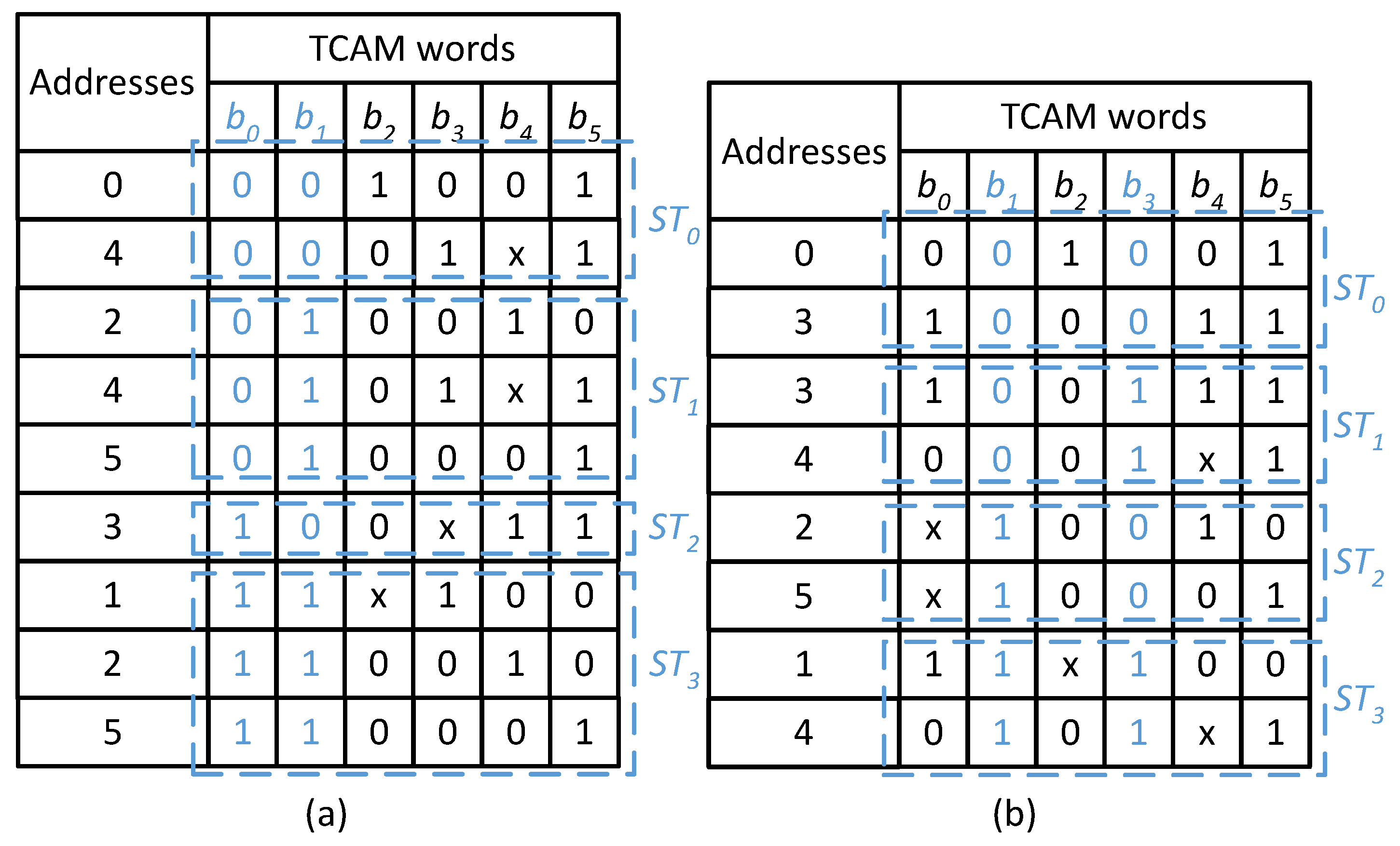
M sub-tables. For example, suppose two bits are used for the classification of a sample TCAM table of size
is presented in
Table 2. The TCAM table presented in
Table 2 is classified using two different set of bit positions
and
as shown in
Figure 2a,b, respectively. The sub-tables constructed based on the bit values (00, 01, 10, and 11) of bit positions
are shown in
Figure 2a. The number of TCAM words in the constructed sub-tables
,
,
and
varies based on the pattern of bits in the bit positions
selected for the classification of
Table 2. TCAM words with ‘x’ as bit value in the classification bit positions are stored in more than one sub-table. For example, the TCAM word at address 2 has the bit values of ‘x1’ at
, and is thus stored in both sub-tables
and
. This redundancy expands the resultant TCAM sub-tables. The classification of any realistic dataset based on a specific set of bit positions may not necessarily produce sub-tables of the same size.
The proposed solution is based on the concept that the classification effectiveness of a set of bit positions varies from that of other bit positions for a specific dataset when the target of the classification is to construct balanced-size sub-tables. The classification example of the TCAM table in
Table 2 using two different sets of bit positions is illustrated in
Figure 2. It shows that the classification using
is more effective for the TCAM table presented in
Table 2, as the constructed sub-tables are of balanced size (2), when compared with the unbalanced size sub-tables constructed for bit positions
(2, 3, 1, and 3) as explained above.
The constructed TCAM sub-tables are further mapped to the distinct rows of SRAM blocks in the proposed design.
Figure 3 shows the mapping of the proposed classification scheme constructed sub-tables to SRAM memory. The contents of the four bit places
of the unbalanced size sub-tables shown in
Figure 2a and that of bit places
of the balanced size sub-tables shown in
Figure 2b are vertically partitioned into width of two, further mapped to the SRAMs with depth
shown in
Figure 3a,b, respectively. It clearly illustrates that the SRAM memory requirement for storing balanced size TCAM sub-tables constructed for bit positions
is lower than that of unbalanced size sub-tables constructed for bit positions
. The SRAM memory utilization overhead for pre-classifying the TCAM table contents in the proposed approach is minimal as balanced size sub-tables are constructed based on effective classification bits.
Algorithm 1 describes the proposed classification scheme. It classifies the TCAM words of the TCAM table into M sub-tables based on the comparison with the -bit values extracted from specific bit positions. The resultant sub-tables formed are tested for the maximum depth bound (MDB) of , where is the width of the configured SRAM blocks of the design on FPGA and is a scaling factor with integer values of . If the number of TCAM words in the resultant sub-tables exceeds MDB, a subsequent set of bit positions is used for the classification of the TCAM table. In the worst-case scenario, all subsets of bit positions from W bit positions are used to classify the TCAM table. The worst-case classification complexity of the proposed Algorithm 1 is reduced by using a relaxed MDB for the construction of sub-tables. An increase in the value of by one increases the MDB of the sub-tables by . A relaxed MDB of the sub-tables results in an increased RAM memory usage, as the resultant sub-tables are mapped to the SRAM blocks of the proposed design. The value of provides a trade-off between the time complexity of the proposed classification algorithm and the overall RAM memory usage of the proposed design.
The words of the M TCAM sub-tables are mapped to the M rows of the SRAM blocks of the architecture and the corresponding classification bit positions are used to configure the pre-classifier bit positions in the proposed architecture.
| Algorithm 1 Algorithm for the classification of the TCAM table into M sub-tables. |
INPUT:D ternary words of W bits: , where x, All possible subsets of bit positions from W bit positions: , where , OUTPUT:M sub-tables (STs) with identification addresses of , and each ST of ternary words of W bits: , where x. fordo for do // Check for the maximum depth bound if () then else // Extraction of classification bits & construction of sub-tables if () then end if end if end for end for : Extracted classification bits : Size of constructed sub-tables
|
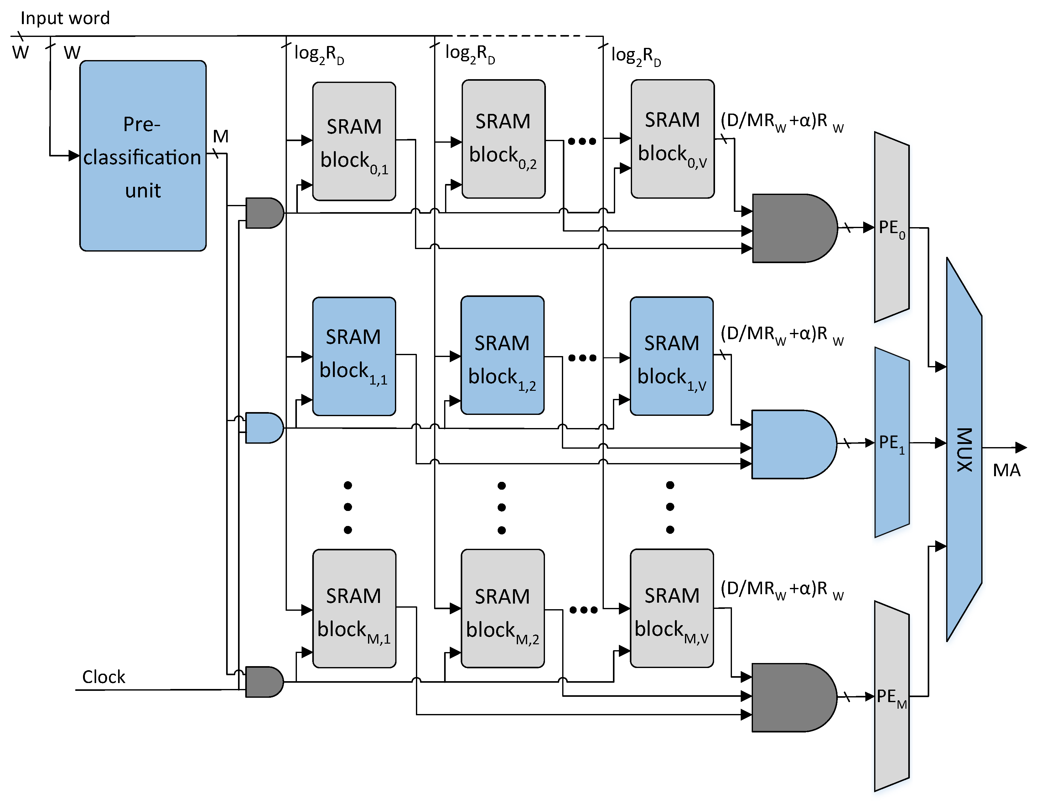
3.2. Proposed Architecture
The TCAM table of size is classified into M sub-tables using the proposed classification scheme in Algorithm 1. The W-bit TCAM words of M sub-tables constructed are further divided into V sub-words of -bits. The resultant sub-partitions of the TCAM table are mapped to the M rows of the V SRAM blocks in the proposed architecture as shown in Figure 5. Each TCAM table sub-partition of size is implemented using an SRAM block. The SRAM block is a cascade of number of size SRAM blocks.
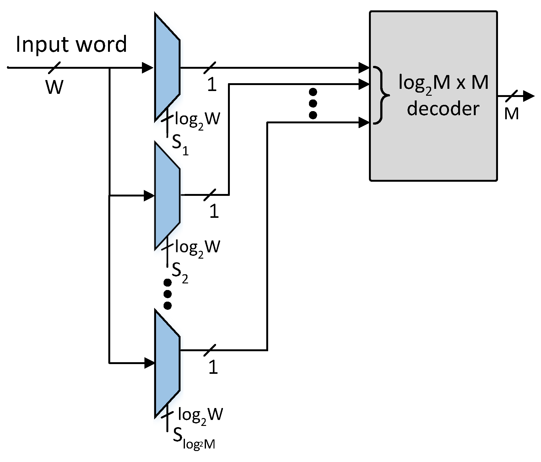
The proposed architecture comprises a pre-classifier unit and an SRAM-based TCAM. The pre-classifier unit of the proposed architecture is shown in
Figure 4. The bit positions of the pre-classifier bits are specified using Algorithm 1 provided
number of pre-classification bit positions. The pre-classifier bits are extracted from the
bit positions of the incoming TCAM words using the
number of select lines of
W-to-1 multiplexers as shown in
Figure 4. The extracted
bits are further decoded to get an
M-bit control signal that selectively activates at most one row of SRAM blocks of the proposed architecture.
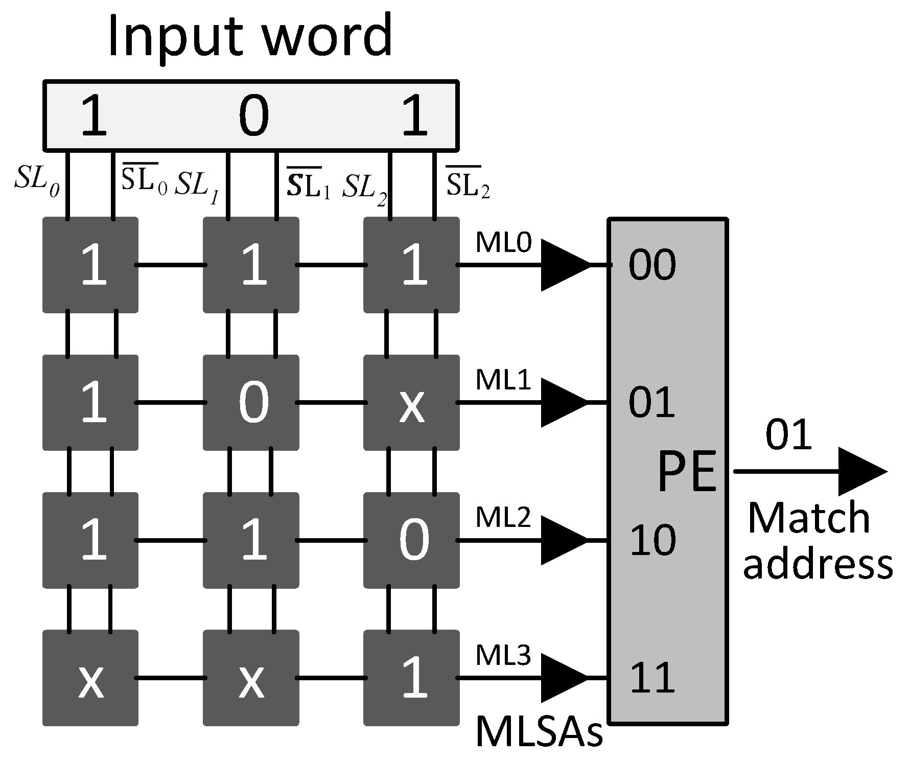
The proposed SRAM-based TCAM architecture is shown in
Figure 5. The incoming
W-bit TCAM word is divided into
V sub-words of
-bits. The
V sub-words are provided as addresses to the selected row of
V SRAM blocks in parallel and
V SRAM words are read. The
V SRAM words read undergo a bit-wise
AND operation and the resultant matching information bit vector is provided to the associated PE. The PE unit encodes the highest-priority matching bit position with the level high as the matching address.
3.3. Update Operation
The proposed TCAM design maps a new TCAM table dataset of the same size to the SRAM blocks of the configured architecture on FPGA. The SRAM blocks of the architecture has storage space for number of -bit TCAM sub-words. Algorithm 1 finds the set of classification bit positions, which makes TCAM sub-tables considering the maximum depth limitation of the configured architecture SRAM blocks on FPGA. The updated TCAM sub-tables are mapped to the SRAM blocks of the design on FPGA. The corresponding classification bit positions from Algorithm 1 configure the pre-classifier unit. The classification bits are now extracted from the updated set of bit positions for the incoming TCAM words. The proposed solution performs reconfiguration of the hardware design on FPGA in two cases: first, when the number of TCAM words in the Algorithm 1 constructed TCAM sub-tables exceeds the storage space of the configured architecture SRAM blocks, resulting in a relaxed MDB on the updated TCAM sub-tables. Second, when a TCAM table of different size is implemented in the proposed design.
During run-time, an update process of a TCAM word in proposed design includes the writing of the update word to the respective TCAM sub-table first, and the updated sub-table is then written to the corresponding row of SRAM blocks in the proposed architecture. The number of TCAM words in updated sub-tables is tested for the MDB of
as this is the storage capacity of a row of configured SRAM blocks in proposed architecture. Owing to the presence of the don’t-care bits (x) in the TCAM words, EE-TCAM in the worst case writes the entire used SRAM memory to complete the update process of a TCAM word. The partitioned sub-tables are written in parallel to the corresponding SRAM blocks in the proposed architecture, and the depth
of the configured BRAMs determines the update latency of EE-TCAM design. The update latency of EE-TCAM is 513 cycles. While native TCAMs have also comparable worst case TCAM write time of O(N) for updating a TCAM word, where N is the number of words in the TCAM table [
28,
29,
30,
31].


