A Broadband THz On-Chip Transition Using a Dipole Antenna with Integrated Balun


Department of Electronic Engineering, Sogang University, Seoul 04107, Korea
*
Author to whom correspondence should be addressed.
Electronics 2018, 7(10), 236; https://doi.org/10.3390/electronics7100236
Submission received: 30 August 2018
/
Revised: 28 September 2018
/
Accepted: 1 October 2018
/
Published: 5 October 2018
Abstract
:A waveguide-to-microstrip transition is an essential component for packaging integrated circuits (ICs) in rectangular waveguides, especially at millimeter-wave and terahertz (THz) frequencies. At THz frequencies, the on-chip transitions, which are monolithically integrated in ICs are preferred to off-chip transitions, as the former can eliminate the wire-bonding process, which can cause severe impedance mismatch and additional insertion loss of the transitions. Therefore, on-chip transitions can allow the production of low cost and repeatable THz modules. However, on-chip transitions show limited performance in insertion loss and bandwidth, more seriously, this is an in-band resonance issue. These problems are mainly caused by the substrate used in the THz ICs, such as an indium phosphide (InP), which exhibits a high dielectric constant, high dielectric loss, and high thickness, compared with the size of THz waveguides. In this work, we propose a broadband THz on-chip transition using a dipole antenna with an integrated balun in the InP substrate. The transition is designed using three-dimensional electromagnetic (EM) simulations based on the equivalent circuit model. We show that in-band resonances can be induced within the InP substrate and also prove that backside vias can effectively eliminate these resonances. Measurement of the fabricated on-chip transition in 250 nm InP heterojunction bipolar transistor (HBT) technology, shows wideband impedance match and low insertion loss at H-band frequencies (220–320 GHz), without in-band resonances, due to the properly placed backside vias.
1. Introduction
The terahertz (THz) wave is generally referred to as the frequency band from 0.1 THz to 10 THz, corresponding to the wavelength in air from 3 mm to 0.03 mm [1]. This frequency band is often called a THz gap, because it has been known to be difficult to generate and detect signals at this frequency band using electronic or optical technologies. Recently, there has been extensive research on THz applications in various fields, such as high-speed communications, non-destructive inspections, spectroscopy, and medical imaging [2,3,4]. THz monolithic integrated circuits (TMICs), such as power amplifiers, multipliers, mixers, and antennas, have been successfully developed using advanced transistor technologies, such as a complementary metal oxide semiconductor (CMOS), gallium arsenide (GaAs) high-electron mobility transistors (HEMTs), and indium phosphide (InP) heterojunction bipolar transistors (HBTs) [5,6,7,8,9,10]. These semiconductor-based technologies allow the production of low-cost, compact, portable, and mass-producible THz systems.
In order to build practical THz systems, it is essential to package the developed TMICs into waveguide modules. Especially rectangular waveguides that are well-suited for THz transmission lines, as they allow low loss and easy fabrication compared with the coaxial cables. There can exist many electromagnetic (EM) modes in rectangular waveguides, the dominant mode with lowest cut-off frequency being a transverse electric (TE10) mode. However, TMICs are implemented with planar transmission lines, such as microstrip lines and coplanar waveguides in a quasi-transverse electromagnetic (TEM) mode. Therefore, transition with a low loss and broad bandwidth is an indispensable component of converting the modes of EM fields between TMICs and rectangular waveguides.
There are several publications on rectangular waveguide-to-microstrip transitions at THz frequencies [11,12,13,14,15]. Off-chip transitions are designed using thin substrates with low loss and low dielectric constant (εr), such as 50-μm-thick quartz with εr = 3.8, allowing a wideband low-loss performance [14,15]. However, they should be electrically connected to TMICs using bond-wires, which lead to parasitic components and result in impedance mismatches and additional losses. In order to minimize the performance degradation of bond-wires, the transitions can be monolithically integrated into TMICs, which are called on-chip transitions [16]. On-chip transitions eliminate the wire-bonding process and additional interconnection lines, which result in compact, low loss, low cost, and highly repeatable THz modules.
However, on-chip transitions can exhibit limited performance. The semi-conductor substrates used in TMICs generally exhibit a high dielectric constant and high loss tangent, compared with those used in off-chip transitions. Note that the waveguide size becomes very small at a THz frequency in order to eliminate higher order EM modes. For example, an internal size of WR-03 waveguide for H-band (220–320 GHz) is only 860 μm × 430 μm, therefore a very thin substrate is preferred for the transitions, which are inserted inside the waveguides. In other words, the transition designed in the thick substrate with a high dielectric constant can increase the impedance mismatch between air-filled waveguide and transition. It can also generate higher order EM modes inside the transition or waveguide, significantly degrading the transition performance. In the work published by Zamora et al. [17], an on-chip transition was designed on very thin (25 μm) InP substrate in a WR-4.3 waveguide (operating frequency = 170–260 GHz, waveguide size = 1.092 mm × 0.546 mm). However, the very thin substrate can cause wafer-handling problems and high fabrication costs. In addition, many backside vias were closely placed in order to reduce the substrate modes in coplanar waveguides, without the detailed analysis of the resonances in the InP substrate [17].
In this work, we design an on-chip rectangular waveguide-to-microstrip transition on a thick InP substrate at the H-band, using a dipole antenna with an integrated balun. We analyze the resonance problem created by the InP substrate using a three-dimensional (3-D) EM simulator. It is demonstrated that the transition can experience severe performance degradation from the resonances induced in the InP substrate. It is also shown that the resonances can be effectively eliminated by properly placing backside vias. Finally, the designed transition was fabricated and measured to show low-loss and resonance-free performance across full H-band frequencies.
2. Design of the On-Chip Transition with an Integrated Balun
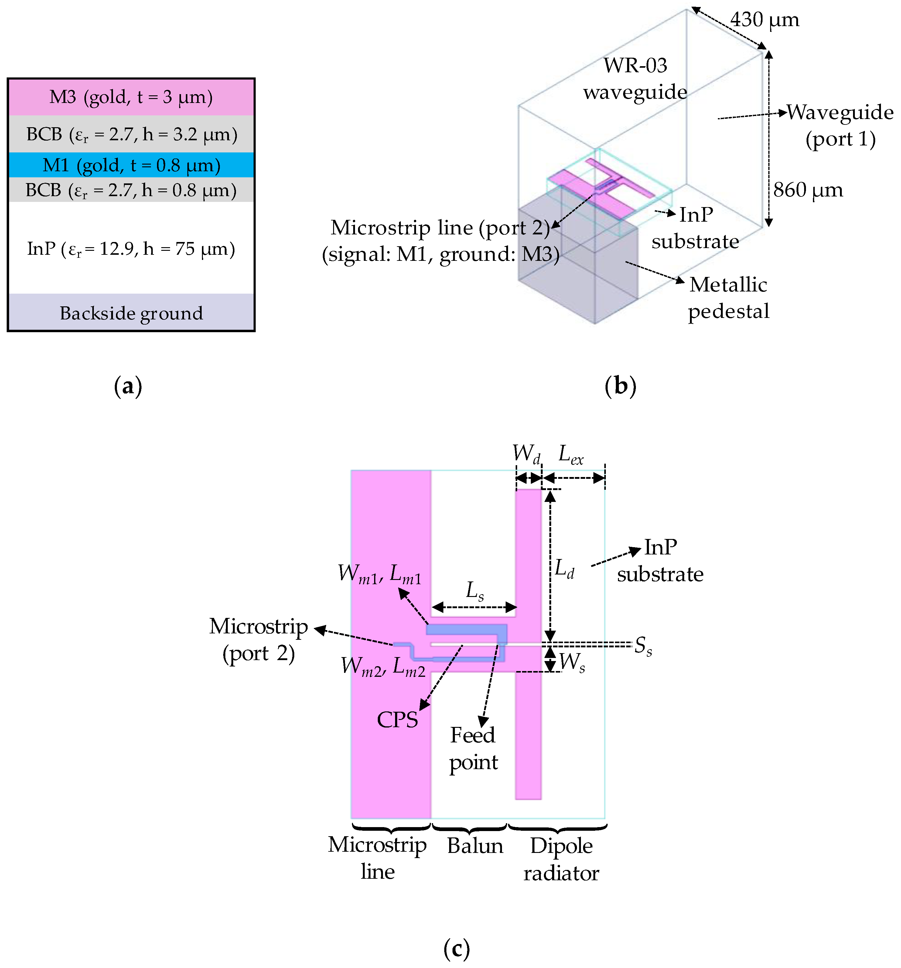
We designed the waveguide-to-microstrip transition using a 250 nm InP HBT process, so that it can be easily integrated with TMICs developed using the same processes [16]. Figure 1a shows the layer structure of this process where active circuits reside on the 75 μm-thick InP substrate (εr = 12.9). Therefore, the backside via connecting the ground of active or passive circuits with the backside ground creates high parasitic inductance and resistance, which leads to severe performance degradation of TMICs at THz frequencies. Generally, one of the front metal layers is utilized as a ground plane of TMICs to minimize parasitic effects [8]. In this work, the third metal layer (M3) is selected as a ground plane, while the first metal layer (M1) is used on the InP substrate as a signal line of microstrip lines connecting the circuit components, such as transistors, resistors, and capacitors. The intermediate metal layer (M2) is omitted in this figure for simplicity. Therefore, the inverted microstrip line is formed between M1 and M3, with the inter-dielectric layer of 3 μm-thick benzocyclobutene (BCB). Several TMICs, such as power amplifiers, were successfully fabricated using this inverted microstrip configuration [10,18].
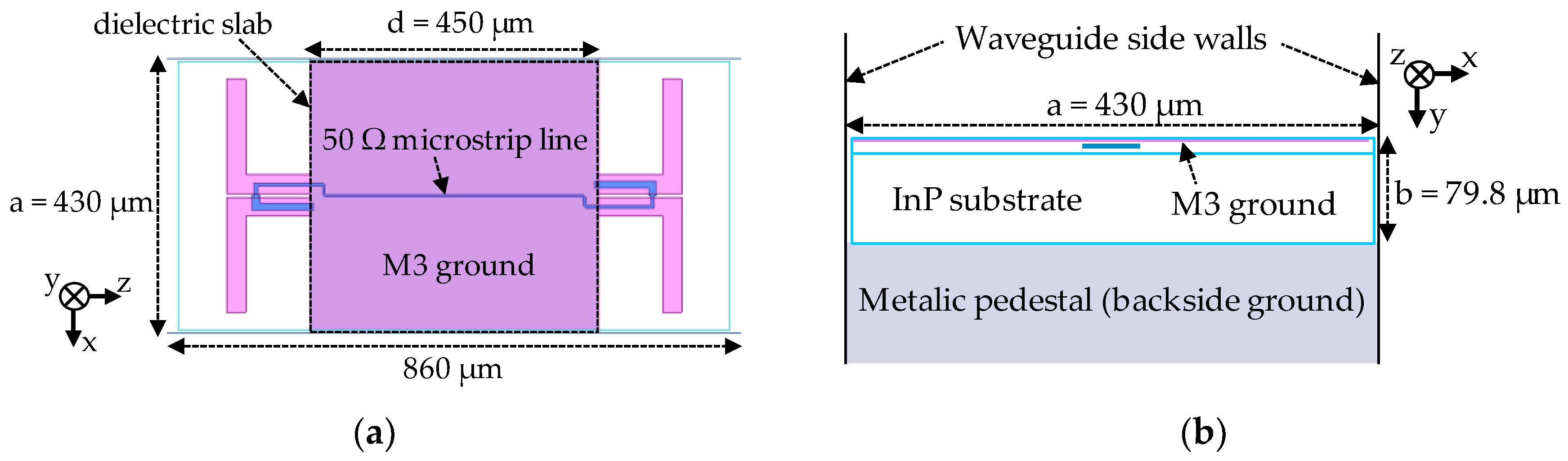
Figure 1b shows the proposed H-band waveguide-to-microstrip transition on the InP substrate using the dipole antenna, which allows for a compact size, simple structure, broad bandwidth characteristics, and alignment of input and output waveguide ports. A detailed layout of the transition is described in Figure 1c, consisting of a dipole radiator, coplanar-strip (CPS) line, reflector, balun, and microstrip line. The rectangular waveguide (WR-03 at H-band) operates at its dominant mode (TE10), presenting electric field intensity parallel to the E-plane of the waveguide [19]. Its EM fields are captured by the dipole radiator (approximately a half-wave long) inducing a differential signal across CPS. The dipole radiator is designed on M3 and connected to the ground plane of microstrip line through CPS line. The ground plane of the microstrip and the metallic pedestal underneath support the transition substrate to operate as a reflector of the dipole antenna. The signals on CPS are then converted to the quasi-TEM of the microstrip line, due to the CPS-to-microstrip transition, which performs the function of the balun, as well as converting differential signals to single-ended signals [20,21].
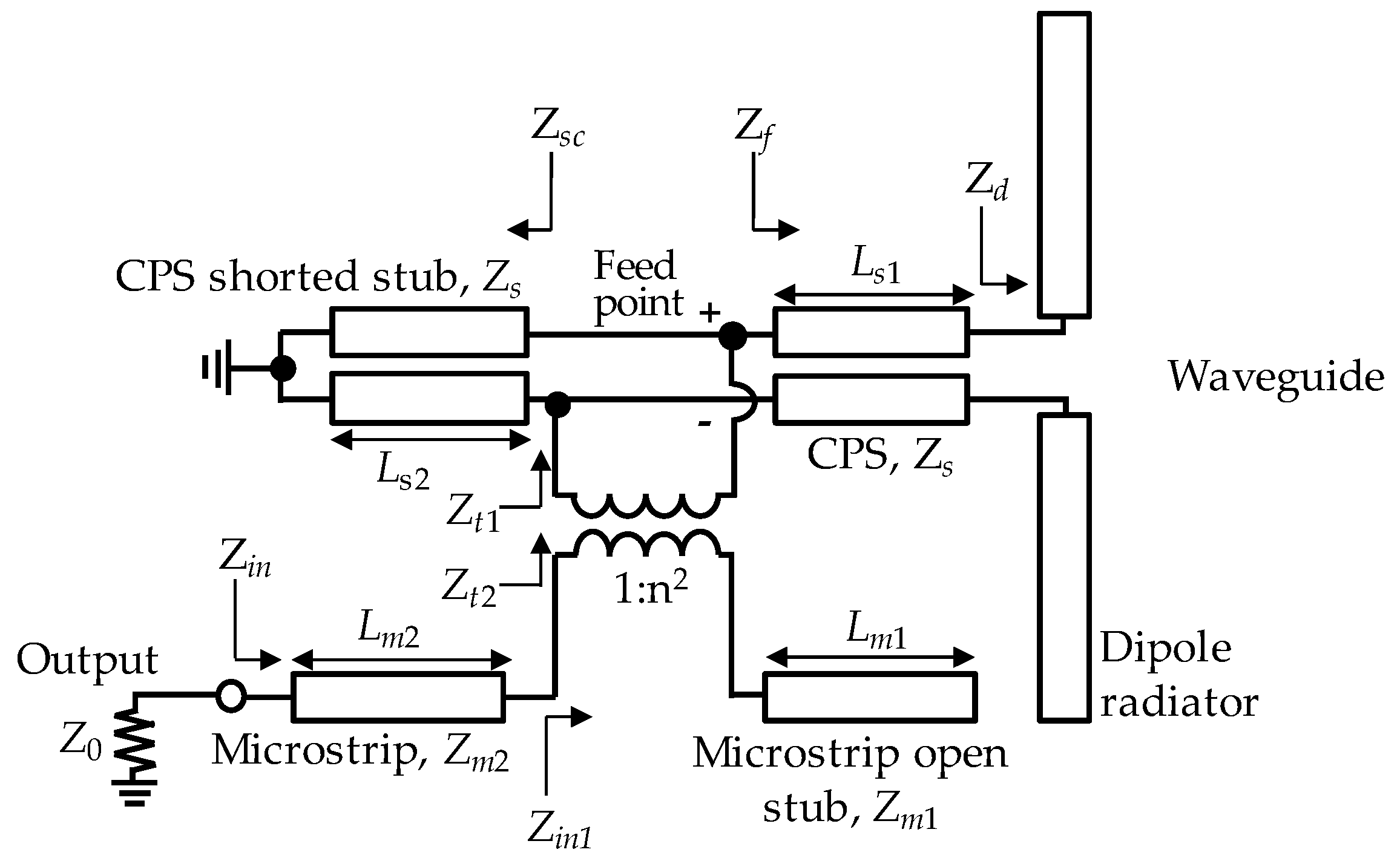
The transition in Figure 1 can be modeled as its equivalent circuit as shown in Figure 2 [20]. The coupling between CPS and microstrip line is represented by an ideal transformer with an impedance transformation ratio of 1:n2. The length of the CPS line (Ls), or the distance between radiator and reflector, is generally determined to be around 0.2× the guided wavelength. According to the design theory of the dipole antenna [22], so that Zsc is expected to provide a high impedance (or open in an ideal case). The microstrip open stub is approximately a quarter-wave long and provides a short circuit to one terminal of the transformer. In this way, the CPS-to-microstrip line provides a function of balun (converting the balanced signal in CPS to an unbalanced one in the microstrip line). The impedances indicated in Figure 2 at each point can be calculated using the transmission line theories as follows [19].
The properties of transmission lines are represented by characteristic impedances (Zs or Zm), propagation constants (βs or βm), and lengths (Ls or Lm). The subscript s and m represent CPS and microstrip line, respectively.
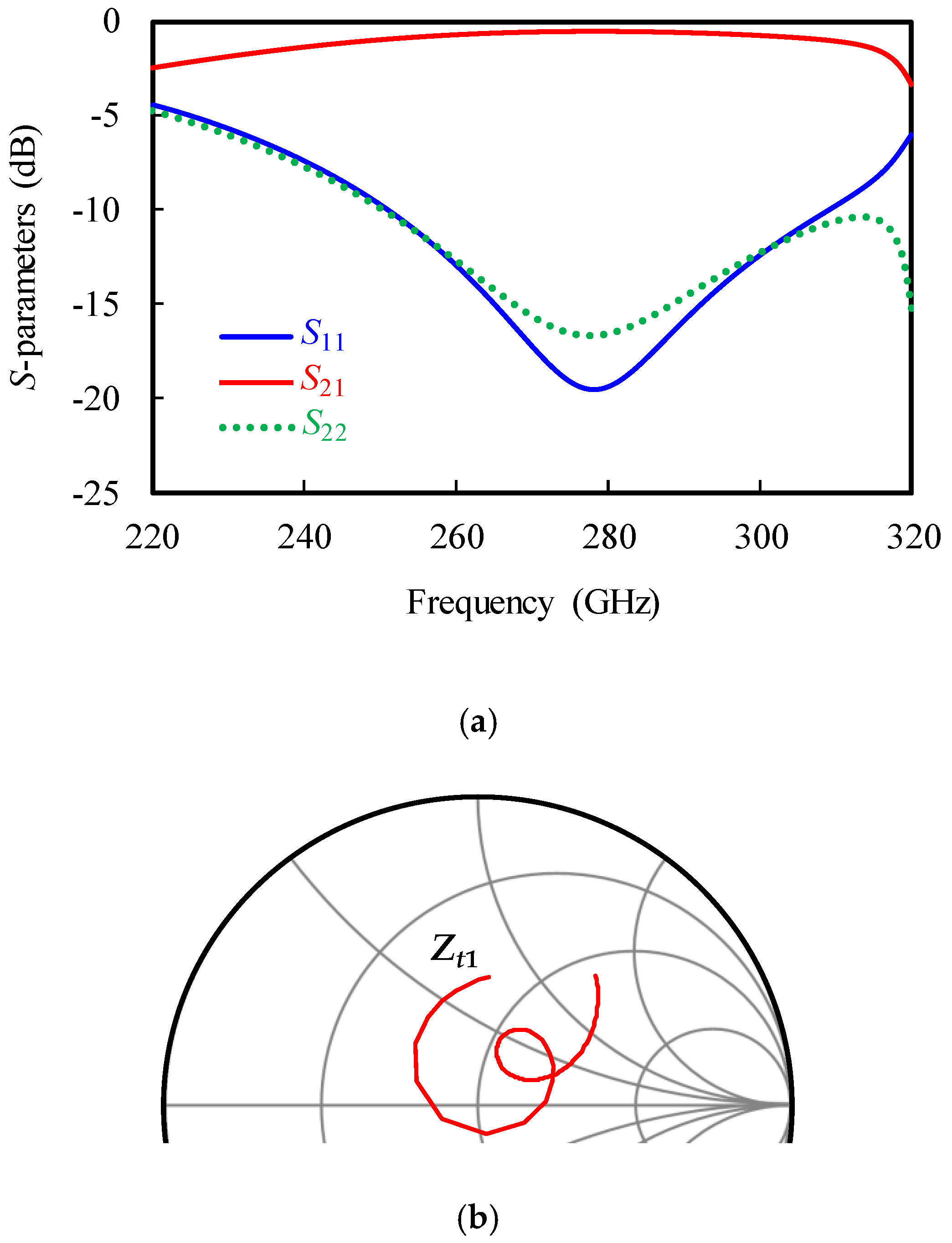
Based on the equivalent circuit model, the dimensions of the transition are mainly determined from the 3-D EM simulation using Ansoft HFSS. Firstly, the simulation is performed on the transition without M1 signal lines to determine the dimensions of the dipole radiator (Wd and Ld), CPS (Ws, Ss, Ls1), and the distance of the dipole radiator from the reflector (Ls). In this simulation, the waveguide is set to port 1 and a differential 50 Ω port 2 is set up across two strips at the distance of Ls1 from the dipole radiator, as illustrated in Figure 2. The latter node is referred to as a feed point of the dipole antenna. The dimensions are then determined from the EM simulation to provide low insertion loss (10log|S21|2) and good impedance match or return loss (−10log|S11|). Figure 3 shows the simulation results of this structure using the determined dimensions given in Table 1, exhibiting insertion loss of 0.54 dB and return loss greater than 15 dB at 280 GHz. Figure 4 shows the simulated Zt1 (impedance at the feed point), indicating that the dipole antenna was properly designed, allowing a broadband impedance match.
Next, we place a microstrip signal line in M1 above the feed point and extend it along the CPS. One end of the microstrip signal line is terminated with the open circuit and the other microstrip output port of the entire transition. The microstrip interconnection line (Zm2 and Lm2) to output port is designed to have a characteristic impedance of Z0 (50 Ω). Dimensions of the microstrip open stub (Wm1 and Lm1) are determined by the EM simulation. From the simulation it is found that the approximately quarter-wave long open stub with low characteristic impedance (about 35 Ω) allows for the most wideband impedance matches.
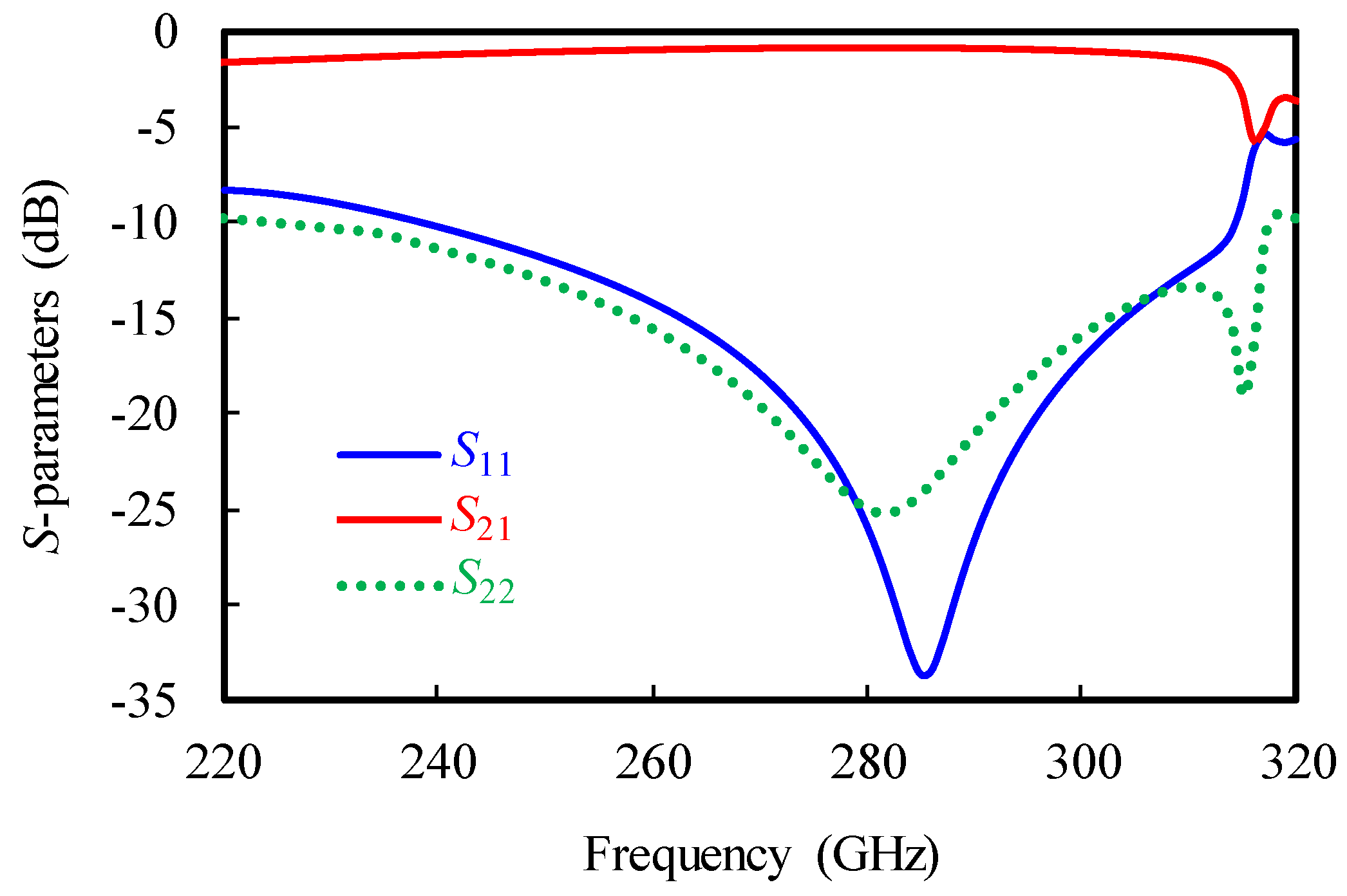
Following the above procedures, we determine all the dimensions of the transition, which are listed in Table 1. Figure 4 shows the simulation results of the designed waveguide-to-microstrip transition (not back-to-back but single transition). Note that in this simulation, input and output ports are waveguide and microstrip, respectively. The designed transition shows insertion loss less than 1.5 dB and return loss greater than 10 dB between 240 and 312 GHz.
3. Resonance Problems of the On-Chip Transition
In Section 2, we designed the single on-chip transition with a short microstrip section as shown in Figure 2. However, TMICs need long microstrip lines for interconnection and impedance matching, which can occupy a large InP area. In addition, they usually require transitions at both input and output, when they are packaged as waveguide modules. Considering this situation, we construct back-to-back connected transitions with a 352 μm-long 50 Ω microstrip line, which resides on the metallic pedestal, as shown in Figure 5a. This 50 Ω microstrip line will be replaced with TMICs.
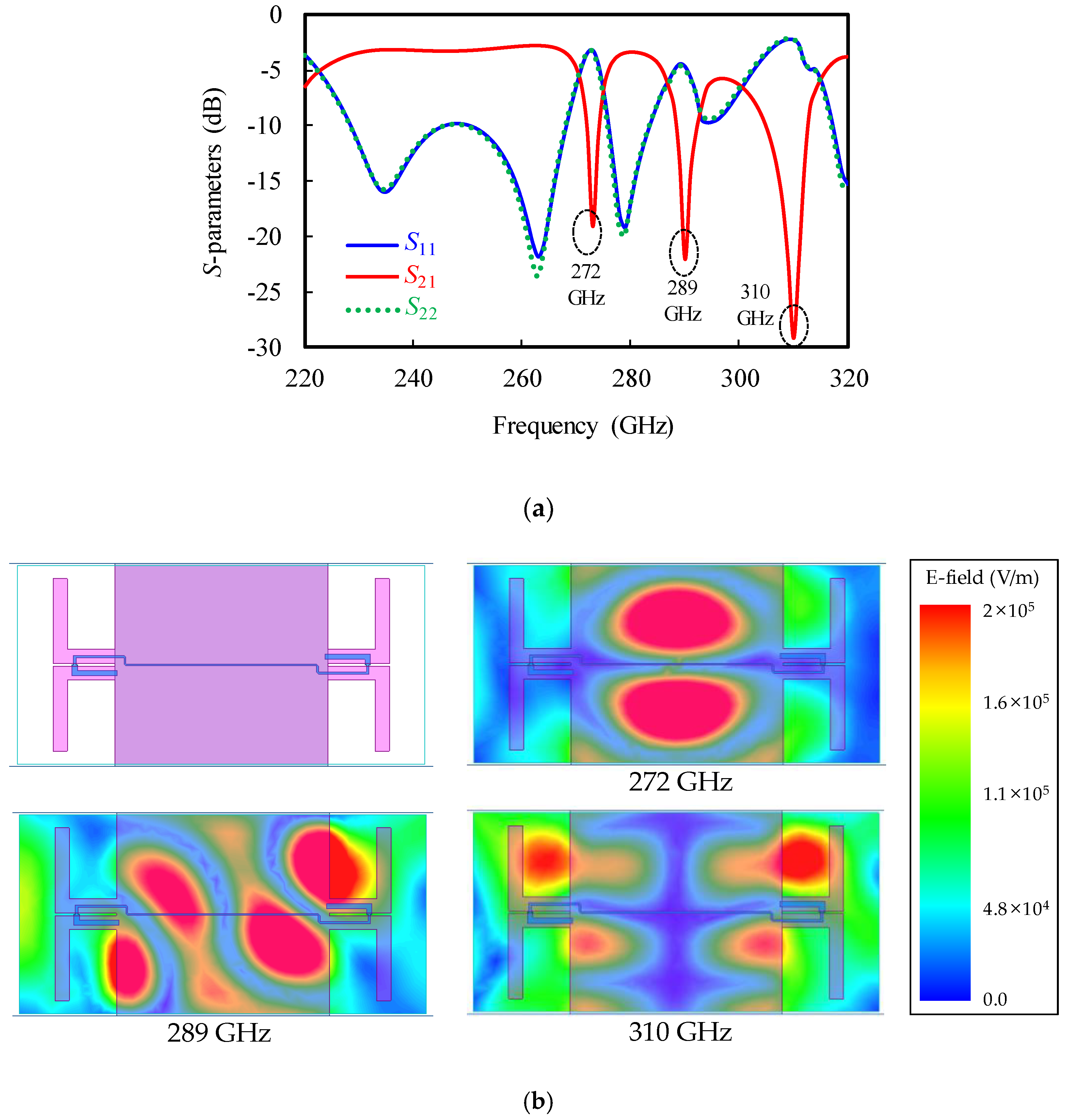
Figure 6a shows the simulation results (S-parameters) of the back-to-back transitions of Figure 5. The dimensions of the transition given in Table 1 were also used in this simulation. Figure 6a demonstrates that the performance of the transition can be severely degraded by simply connecting two transitions in the back-to-back configuration, due to several in-band resonances at 272, 289, and 310 GHz. Note that most of these were not found in the simulation results of the single transition (Figure 4). Figure 6b shows the magnitude of electric field intensity in the middle plane of InP substrate at each resonance frequency. These plots illustrate that EM energies are confined in the InP substrate at resonant frequencies, so we can claim that the resonances are related to the dielectric slab. This InP slab is covered with M3 and backside ground planes on the top and bottom, respectively, and waveguide side walls on the upper and lower sides, as shown in Figure 5b. That is, the dielectric slab is covered with metals except for the left and right side walls, and can therefore be viewed as a dielectric-filled rectangular waveguide with reduced height. This may result in several resonant frequencies depending on a, b, and d, which are the width, height, and length of the dielectric-filled rectangular waveguide, as designated in Figure 5b.
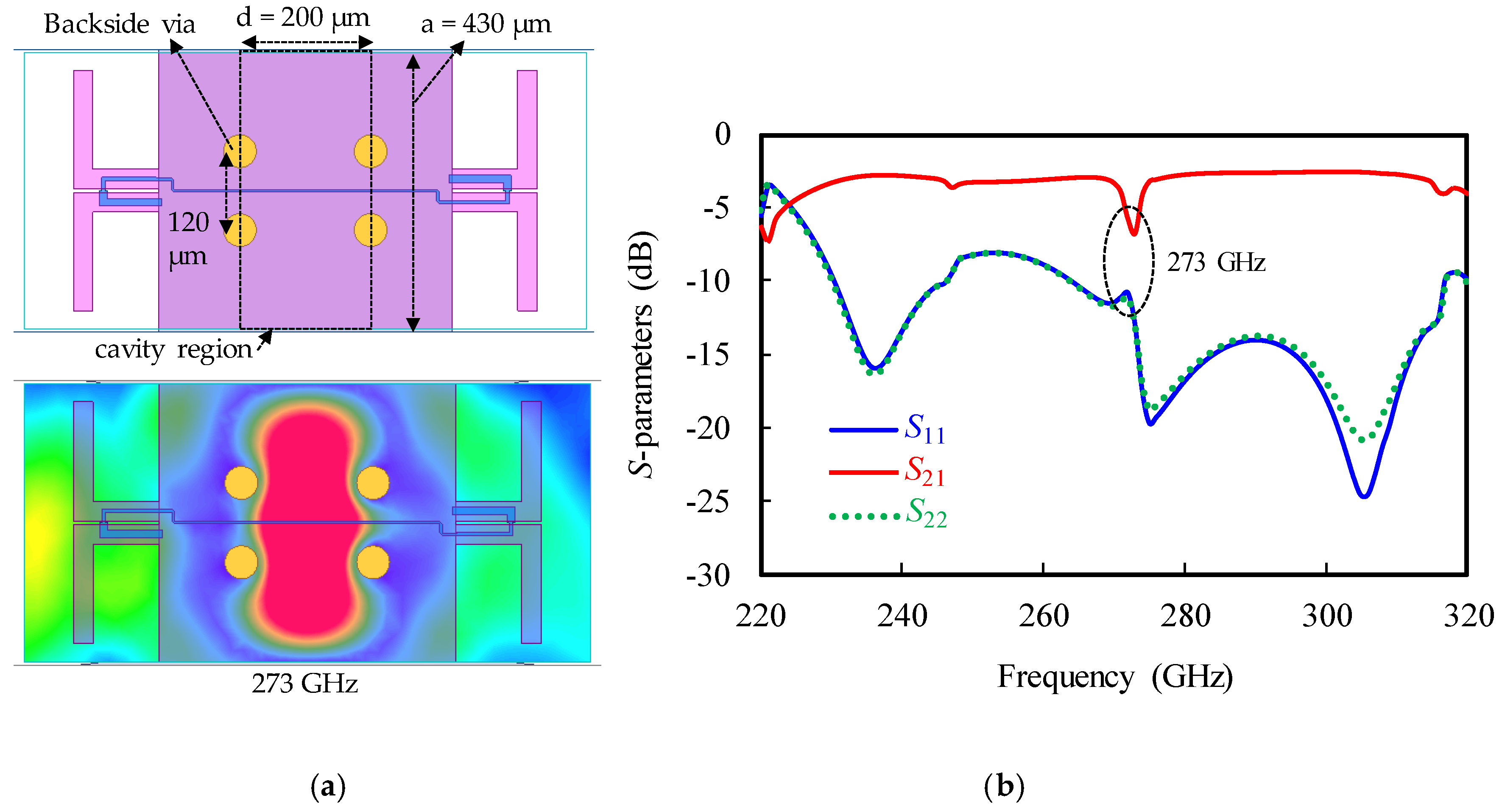
These in-band resonances should be removed so that they do not degrade the performance of TMICs modules when the TMICs are packaged using the transitions. In this work, we utilize the backside vias connecting M3 and backside ground planes to remove the resonances in the dielectric slab. For example, if four backside vias are placed in the dielectric slab as shown in Figure 7a, almost all of the in-band resonances shown in Figure 6 are eliminated, as shown in Figure 7b. This result indicates that the backside vias can suppress the resonances by electrically shorting the fields in the dielectric-filled waveguide. However, there is still a resonance at 273 GHz. This seems to be caused by a rectangular cavity as indicated in Figure 7a, consisting of four backside vias serving as shorting posts of the dielectric-filled waveguide. The resonant frequency of the rectangular cavity filled with a dielectric can be calculated using Equation (6) [23].
where μ and ε denote the permeability and permittivity of the dielectric. There can exist a number of resonance modes depending on the integer values of m, n, and p. Electric field distribution at resonant frequency is plotted in Figure 7a, which is similar to that of TE101 mode (which is a dominant mode in this structure). The four vias are placed apart by 120 and 200 μm in x- and z-axis directions, respectively, which creates the rectangular cavity with a = 430 μm, b = 79.8 μm, and d = 160 μm (with the via diameter considered). The resonant frequency can be calculated to be 278 GHz from Equation (6), which is very close to the simulation result in Figure 7.
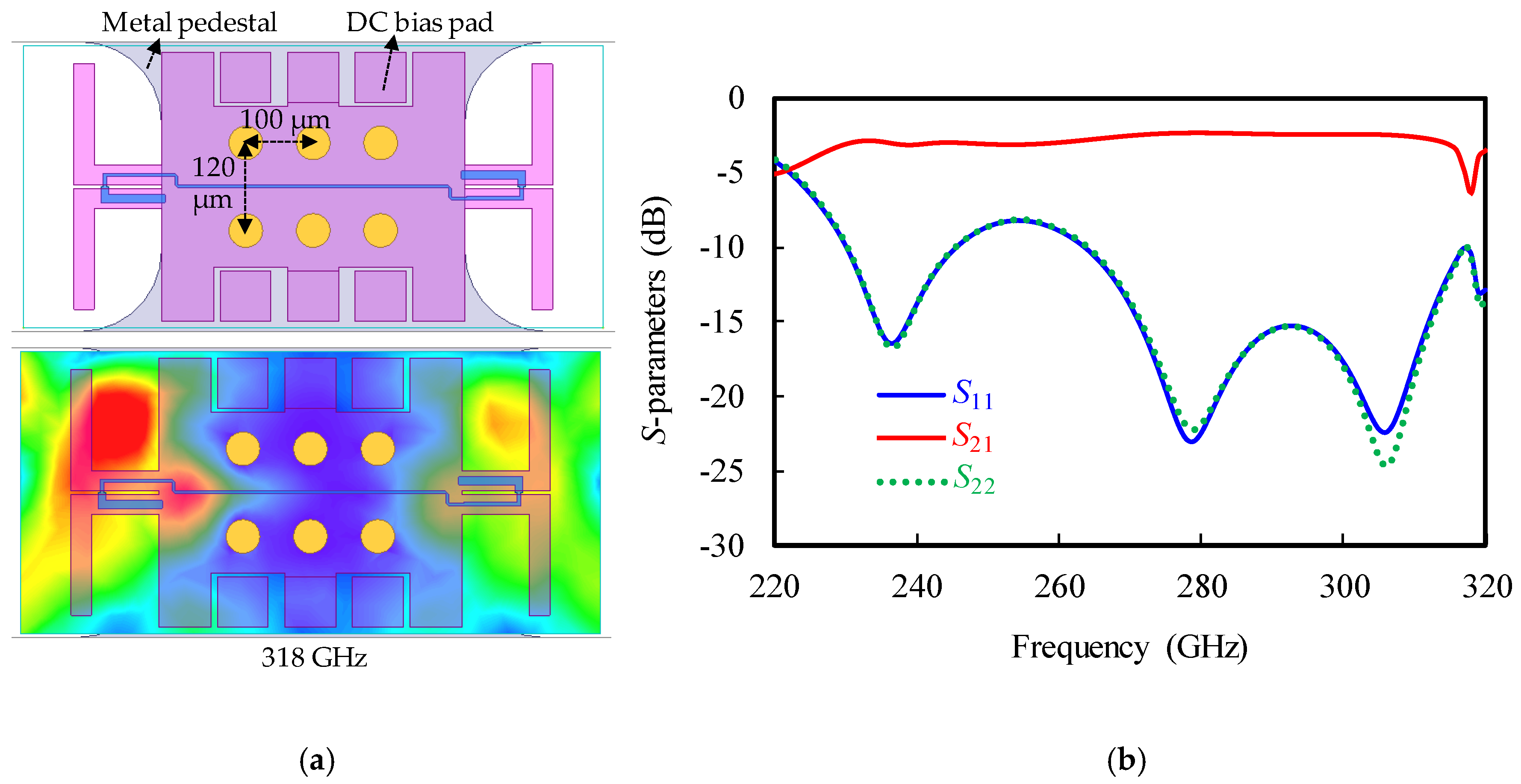
In order to remove all of the resonances, the vias should be placed such that the TE101 mode resonant frequency of the cavity exceeds the upper-edge of the H-band. A cavity with a = d = 185 μm and b = 79.8 μm exhibits the resonance frequency of 319 GHz according to Equation (6). This implies that there will be no in-band resonance if the vias are placed such that the cavity size (a and d) is smaller than 185 μm.
Figure 8a shows the final design of the back-to-back on-chip transition with six backside vias placed properly, such that there is no in-band resonance (with the respective spacing of vias of 120 and 100 μm in x- and z-directions). Typical DC bias and ground pads of TMICs are also included in the layout. The metallic pedestal is drawn to have rounded corners considering the limitation of mechanical machining. Figure 8b shows the simulation results of the final design of the on-chip dipole transition. It shows a back-to-back insertion loss less than 3.0 dB and return loss greater than 8 dB without the resonances from 231 GHz to 314 GHz. There is a small resonance at 318 GHz, which is generated in the space between the dipole radiator and the metallic pedestal, as shown in Figure 8a. The distance between the radiator and reflector can be adjusted to remove this resonance, however this will lead to significant performance degradation of the dipole antenna.
In the above simulations of the back-to-back transition, there is a small difference between S11 and S22. This is because, despite the structure being symmetric, the generated meshes from the EM simulator may not be. Note that the field distribution is time-varying and was captured at the time when the resonant field was obviously observed in the simulation.
4. Experimental Results
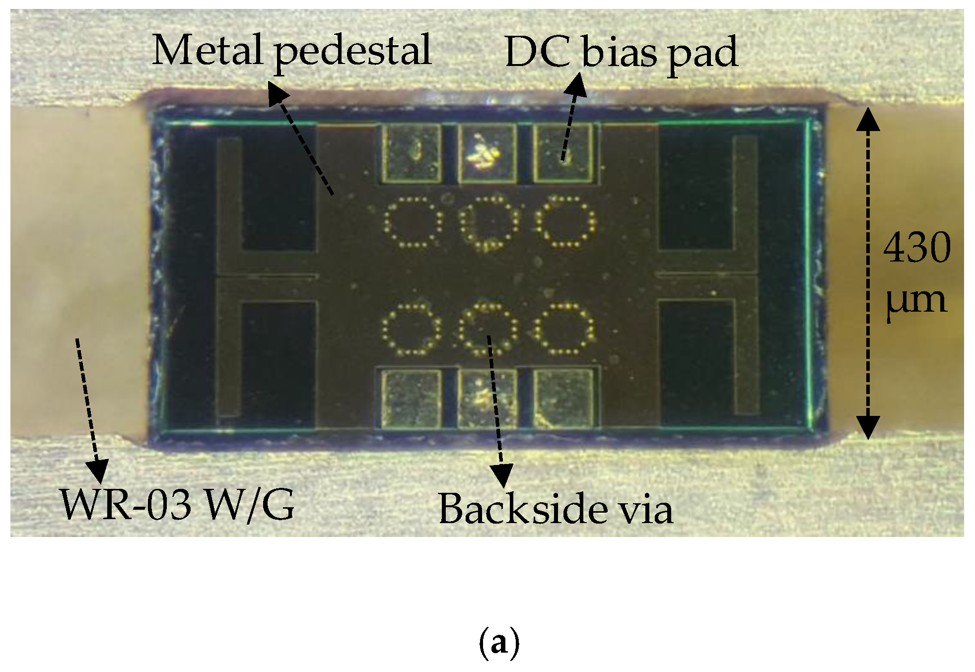
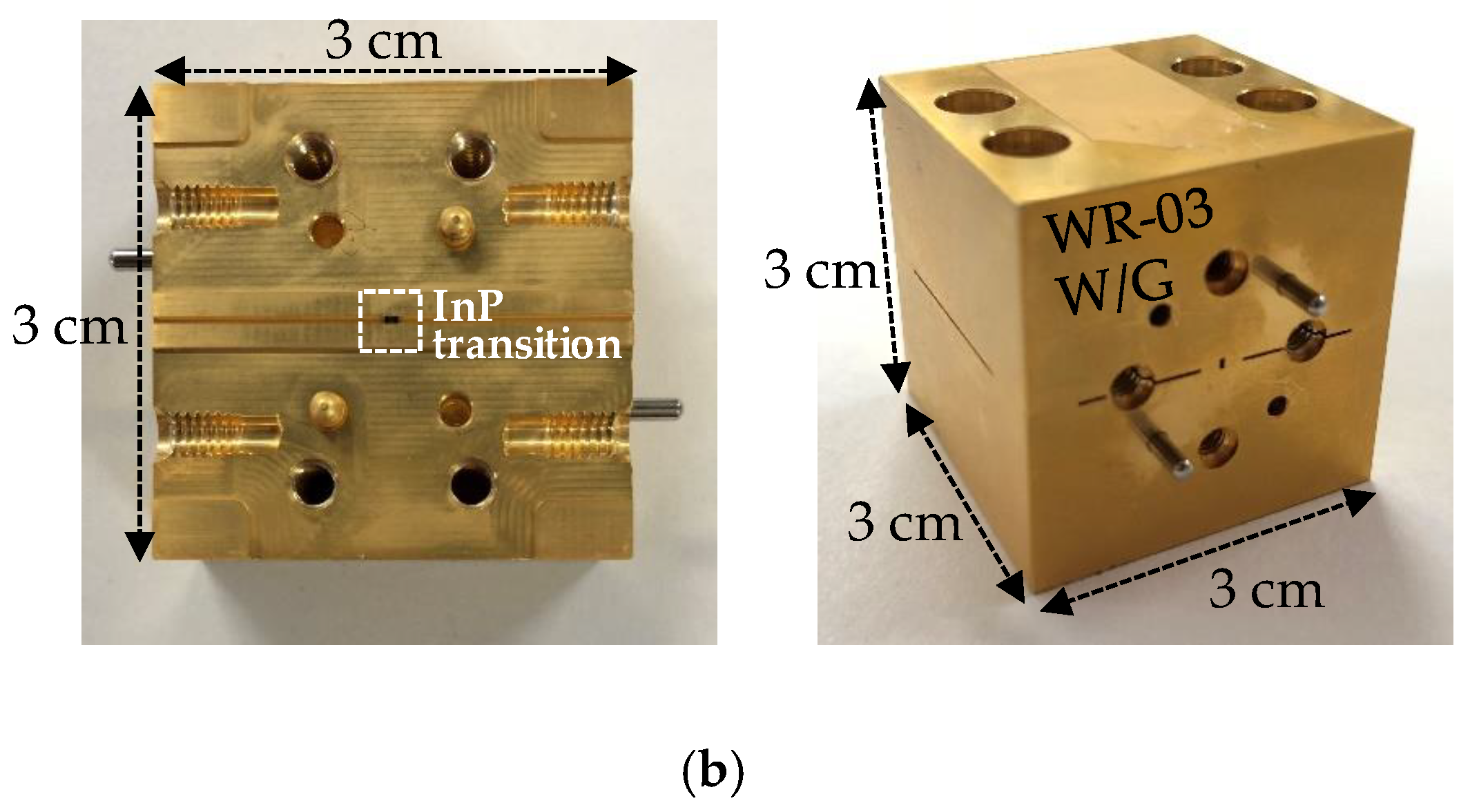
Figure 9a shows the photograph of the fabricated on-chip transition using the 250 nm InP HBT process from Teledyne Technologies (Thousand Oaks, CA, USA). The dipole antennas are fabricated in M3 and the microstrip signal line in M1, under the M3 ground plane. The transition substrate is mounted on the metallic pedestal using a conductive epoxy inside the WR-03 rectangular waveguide, which consists of two split-metallic blocks, as shown in Figure 9b. The size of the module is 3.0 cm × 3.0 cm × 3.0 cm. In order to estimate the loss of the rectangular waveguide itself at H-band, a 3 cm-long straight (through) waveguide was also fabricated and measured.
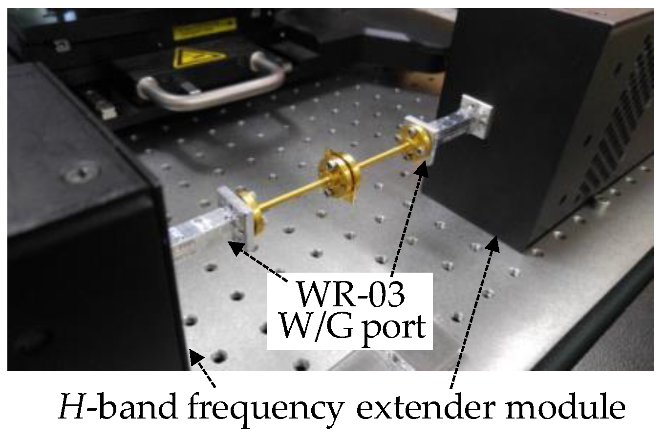
The S-parameters of the fabricated transition were measured using the set up shown in Figure 10, where the H-band frequency extender modules, having WR-03 waveguide flanges, are connected to the vector network analyzer. The fabricated transition module is inserted between the waveguide ports of the extender modules. Prior to measuring the fabricated transition, the calibration was performed by using the WR-03 through-reflect-line calibration standards.
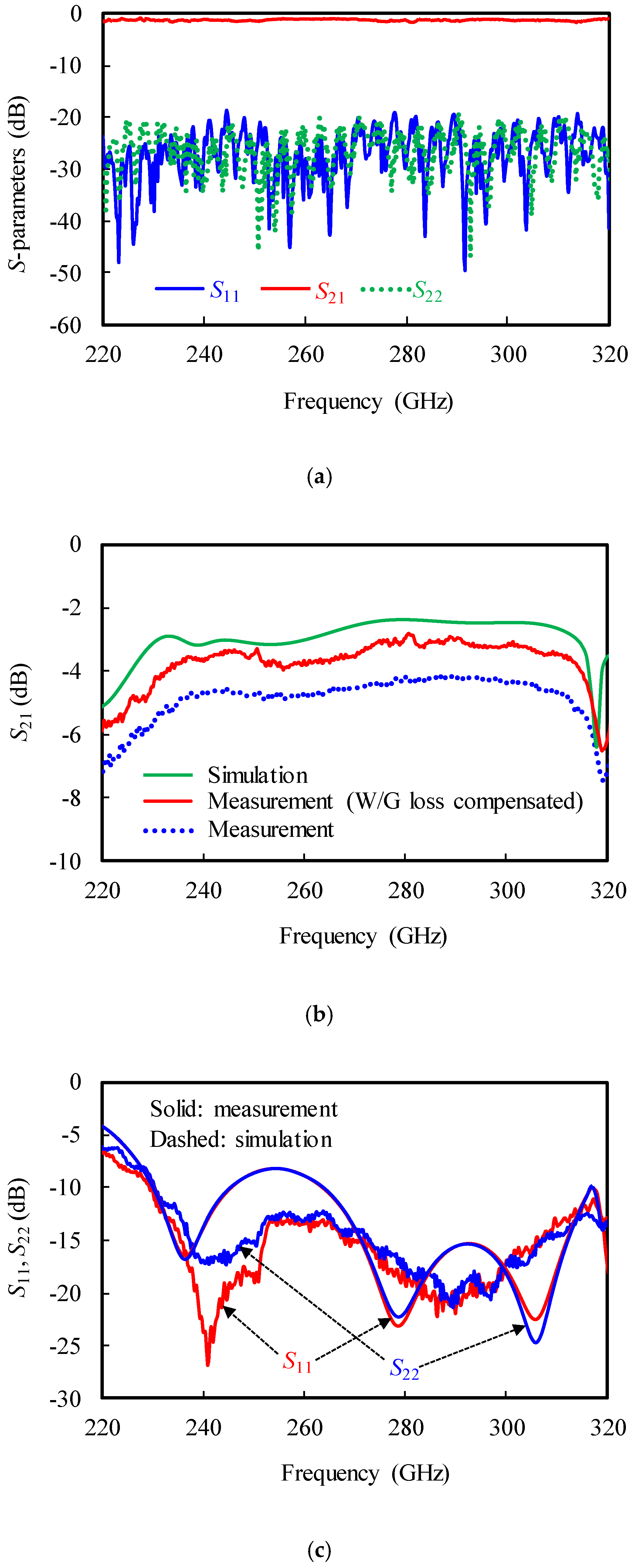
Figure 11a shows the measured results of the fabricated 3 cm-long straight waveguide. It exhibits an insertion loss of 1.0–1.6 dB and return loss greater than 20 dB at full H-band. Figure 11b,c shows the measurement results of the fabricated back-to-back transition, where insertion loss is less than 4.9 dB and return loss is greater than 12 dB, between 235 GHz and 312 GHz. The measurement shows good agreement with the simulation. The small discrepancy seems to be caused by the errors in the fabrication process, such as the substrate attachment and the waveguide machining. Note that there is no in-band resonance as expected by the simulation. Figure 11b also includes the compensated insertion loss, which is obtained by subtracting the measured insertion loss of the 3 cm-long straight waveguide. The compensated insertion loss is 3.2 dB at 300 GHz. A 352 μm-long 50 Ω microstrip line in the middle of two transitions exhibits a 0.95 dB loss from EM simulation. Thus, the insertion loss per transition can be estimated to be as low as 1.1 dB at 300 GHz, which is low enough to be used for packaging TMICs. In summary, the designed InP on-chip transition using dipole antenna with an integrated balun presents low insertion loss and good return loss over a wide bandwidth at H-band, due to the proposed technique of removing in-band resonances.
5. Conclusions
In this paper, the InP on-chip transition operating H-band frequencies (220–320 GHz), was proposed using the dipole antenna with integrated balun. Its structure was designed to provide wideband impedance match and low insertion loss using a 3-D EM simulator. In-band resonance problems were also investigated within the thick InP substrate with high dielectric constant. The simulation and measurement show that these resonances can be removed out of H-band by properly locating several backside vias. The final design of the back-to-back transition showed good wideband impedance match and low loss at H-band. Therefore, it can be effectively integrated on TMICs, such as power amplifiers, low noise amplifiers, oscillators, mixers, and so on, which will allow high performance, low-cost, compact, and reproducible THz modules.
Author Contributions
Conceptualization, W.C. and J.J.; methodology, J.J.; software, W.C.; validation, W.C. and J.J.; formal analysis, W.C.; investigation, W.C.; resources, J.J.; data curation, W.C.; writing-original draft preparation, W.C. and J.J.; writing-review and editing, W.C. and J.J.; visualization, W.C.; supervision, J.J.; funding acquisition, J.J.
Funding
This work was partly supported by a grant to the Terahertz Electronic Device Research Laboratory, funded by Defense Acquisition Program Administration and by the Agency for Defense Development (UD180025RD). This work was also partly supported by the Institute for Information & Communications Technology Promotion (IITP) grant, funded by the Korean government (MSIT) (No. 2016-0-00185, Development of ultra-wideband terahertz CW spectroscopic imaging systems based on electronic devices).
Conflicts of Interest
The authors declare no conflicts of interest.
References
- Sirtori, C. Bridge for the terahertz gap. Nature 2002, 417, 132–133. [Google Scholar] [CrossRef] [PubMed]
- Marchese, L.E.; Terroux, M.; Bolduc, M.; Cantin, M.; Martin, O.; Desnoyers, N.; Bergeron, A. A 0.1 megapixel THz camera with 17 degree field of view for large area single shot imaging. In Proceedings of the 2014 39th International Conference on Infrared, Millimeter, and Terahertz waves (IRMMW-THz), Tucson, AZ, USA, 14–19 September 2014. [Google Scholar]
- Kašalynas, I.; Venckevičius, R.; Minkevičius, L.; Wahaia, F.; Janonis, V.; Tamošiūnas, V.; Seliuta, D.; Valušis, G.; Sešek, A.; Trontelj, J.; et al. High spatial resolution terahertz imaging of carcinoma tissues at 0.6 THz frequencies. In Proceedings of the 2016 41st International Conference on Infrared, Millimeter, and Terahertz Waves (IRMMW-THz), Copenhagen, Denmark, 25–30 September 2016. [Google Scholar]
- Mendis, R. Guided-wave THz time-domain spectroscopy of highly doped silicon using parallel-plate waveguides. Electron. Lett. 2006, 42, 19–27. [Google Scholar] [CrossRef]
- Lee, I.; Kim, J.; Jeon, S. A G-Band Frequency Doubler Using a Commercial 150 nm GaAs pHEMT Technology. J. Electromagn. Eng. Sci. 2017, 17, 147–152. [Google Scholar] [CrossRef] [Green Version]
- Hussain, N.; Kedze, K.E.; Park, I. Performance of a Planar Leaky-Wave Slit Antenna for Different Values of Substrate Thickness. J. Electromagn. Eng. Sci. 2017, 17, 202–207. [Google Scholar] [CrossRef] [Green Version]
- Kim, H.; Choe, W.; Jeong, J. Terahertz CMOS V-shaped Patch Antenna using Defected Ground Structure. Sensors 2018, 18, 2432. [Google Scholar] [CrossRef] [PubMed]
- Kim, J.; Jeon, S.; Kim, M.; Urteaga, M.; Jeong, J. H-Band Power Amplifier Integrated Circuits Using 250-nm InP HBT Technology. IEEE Trans. THz Sci. Technol. 2015, 5, 215–222. [Google Scholar] [CrossRef]
- Kim, J.; Jeong, J. Submillimeter-wave InP HBT power amplifier using impedance-transforming two-way balun. Microw. Opt. Technol. Lett. 2015, 57, 1831–1834. [Google Scholar] [CrossRef]
- Kim, S.; Yun, J.; Yoon, D.; Kim, M.; Rieh, J.; Urteaga, M.; Jeon, S. 300 GHz Integrated Heterodyne Receiver and Transmitter With On-Chip Fundamental Local Oscillator and Mixers. IEEE Trans. THz Sci. Technol. 2015, 5, 92–101. [Google Scholar] [CrossRef]
- Varonen, M.; Samoska, L.; Fung, A.; Padmanahban, S.; Kangaslahti, P.; Lai, R.; Sarkozy, S.; Soria, M.; Owen, H. LNA modules for the WR4 (170–260 GHz) frequency range. In Proceedings of the 2014 IEEE MTT-S International Microwave Symposium (IMS2014), Tampa, FL, USA, 1–6 June 2014. [Google Scholar]
- Varonen, M.; Samoska, L.; Fung, A.; Padmanabhan, S.; Kangaslahti, P.; Lai, R.; Sarkozy, S.; Soria, M.; Owen, H.; Reck, T.; et al. A WR4 Amplifier Module Chain With an 87 K Noise Temperature at 228 GHz. IEEE Microw. Compon. Lett. 2015, 25, 58–60. [Google Scholar] [CrossRef]
- Tessmann, A.; Leuther, A.; Hurm, V.; Massler, H.; Zink, M.; Kuri, M.; Riessle, M.; Lösch, R.; Schlechtweg, M.; Ambacher, O. A 300 GHz mHEMT amplifier module. In Proceedings of the 2009 IEEE International Conference on Indium Phosphide & Related Materials, Newport Beach, CA, USA, 10–14 May 2009. [Google Scholar]
- Choe, W.; Kim, J.; Jeong, J. Full H-band waveguide-to-coupled microstrip transition using dipole antenna with directors. IEICE Electron. Express 2017, 14, 1–6. [Google Scholar] [CrossRef]
- Kim, J.; Choe, W.; Jeong, J. Submillimeter-Wave Waveguide-to-Microstrip Transitions for Wide Circuits/Wafers. IEEE Trans. THz Sci. Technol. 2017, 7, 440–445. [Google Scholar] [CrossRef]
- Samoska, L.; Deal, W.R.; Chattopadhyay, G.; Pukala, D.; Fung, A.; Gaier, T.; Soria, M.; Radisic, V.; Mei, X.; Lai, R. A Submillimeter-Wave HEMT Amplifier Module With Integrated Waveguide Transitions Operating Above 300 GHz. IEEE Trans. Microw. Theory Tech. 2008, 56, 1380–1388. [Google Scholar] [CrossRef]
- Zamora, A.; Leong, K.M.K.H.; Reck, T.; Chattopadhyay, G.; Deal, W. A 170–280 GHz InP HEMT low noise amplifier. In Proceedings of the 2014 39th International Conference on Infrared, Millimeter, and Terahertz waves (IRMMW-THz), Tucson, AZ, USA, 14–19 September 2014. [Google Scholar]
- Song, H.; Kim, J.; Ajito, K.; Kukutsu, N.; Yaita, M. 50-Gb/s Direct Conversion QPSK Modulator and Demodulator MMICs for Terahertz Communications at 300 GHz. IEEE Trans. Microw. Theory Tech. 2014, 62, 600–609. [Google Scholar] [CrossRef]
- Pozar, D.M. Microwave Engineering, 4th ed.; Wiley: New York, NY, USA, 2011; pp. 50–120. [Google Scholar]
- Li, R.; Wu, T.; Pan, B.; Lim, K.; Laskar, J.; Tentzeris, M.M. Equivalent-Circuit Analysis of a Broadband Printed Dipole With Adjusted Integrated Balun and an Array for Base Station Applications. IEEE Trans. Antennas Propag. 2009, 57, 2180–2184. [Google Scholar] [CrossRef] [Green Version]
- Kaneda, N.; Qian, Y.; Itoh, T. A Broad-Band Microstrip-to-Waveguide Transition Using Quasi-Yagi Antenna. IEEE Trans. Microw. Theory Tech. 1999, 47, 2562–2567. [Google Scholar] [CrossRef]
- Stutzman, W.L. Antenna Theory and Design, 3rd ed.; Wiley: New York, NY, USA, 2005; pp. 220–250. [Google Scholar]
- Cheng, D.K. Field and Wave Electromagnetics, 2nd ed.; Addison-Wesley: Boston, MA, USA, 1989; pp. 582–588. [Google Scholar]
Figure 1.
Proposed on-chip waveguide-to-microstrip transition. (a) Layer structure of 250 nm InP heterojunction bipolar transistor (HBT) process. (b) 3-D view of the transition. (c) Detailed view of the transition substrate.
Figure 1.
Proposed on-chip waveguide-to-microstrip transition. (a) Layer structure of 250 nm InP heterojunction bipolar transistor (HBT) process. (b) 3-D view of the transition. (c) Detailed view of the transition substrate.

Figure 2.
Equivalent circuit of the transition.

Figure 3.
Simulation results of the designed dipole antenna without microstrip lines (port 1: Waveguide, port 2: Differential port across two strips on a coplanar strip (CPS) line at a feed point). (a) S-parameters; (b) Zt1.
Figure 3.
Simulation results of the designed dipole antenna without microstrip lines (port 1: Waveguide, port 2: Differential port across two strips on a coplanar strip (CPS) line at a feed point). (a) S-parameters; (b) Zt1.

Figure 4.
Simulation results of the designed transition (single transition).

Figure 5.
Back-to-back structure of the designed on-chip transitions. (a) Top view. (b) Cross-sectional view.
Figure 5.
Back-to-back structure of the designed on-chip transitions. (a) Top view. (b) Cross-sectional view.

Figure 6.
Simulation results of the back-to-back transition. (a) S-parameters. (b) Magnitude of electric field intensity (E-field in V/m) in the middle plane of Indium phosphide (InP) substrate.
Figure 6.
Simulation results of the back-to-back transition. (a) S-parameters. (b) Magnitude of electric field intensity (E-field in V/m) in the middle plane of Indium phosphide (InP) substrate.

Figure 7.
Simulation results of the back-to-back transition with four backside vias. (a) Transition with four backside vias and electric field distribution. (b) Simulated S-parameters.
Figure 7.
Simulation results of the back-to-back transition with four backside vias. (a) Transition with four backside vias and electric field distribution. (b) Simulated S-parameters.

Figure 8.
Final design of the back-to-back transition. (a) Transition with six backside vias and electric field distribution at 318 GHz. (b) Simulated S-parameters.
Figure 8.
Final design of the back-to-back transition. (a) Transition with six backside vias and electric field distribution at 318 GHz. (b) Simulated S-parameters.

Figure 9.
Fabricated waveguide-to-microstrip transition. (a) Fabricated transition in 250 nm InP heterojunction bipolar transistor (HBT) process. (b) Transition mounted in WR-03 rectangular waveguide.
Figure 9.
Fabricated waveguide-to-microstrip transition. (a) Fabricated transition in 250 nm InP heterojunction bipolar transistor (HBT) process. (b) Transition mounted in WR-03 rectangular waveguide.


Figure 10.
Photograph of the H-band measurement set up.

Figure 11.
Measured S-parameters. (a) Fabricated 3-cm-long straight waveguide. (b) Fabricated back-to-back transition (S21). (c) Fabricated back-to-back transition (S11, S22).
Figure 11.
Measured S-parameters. (a) Fabricated 3-cm-long straight waveguide. (b) Fabricated back-to-back transition (S21). (c) Fabricated back-to-back transition (S11, S22).


Table 1.
Dimensions of the designed transition (in μm).
| Lex | Wd | Ld | Ws | Ls | Ss | Wm1 | Lm1 | Wm2 | Lm2 |
|---|---|---|---|---|---|---|---|---|---|
| 75 | 30 | 180 | 30 | 100 | 5 | 11.7 | 105 | 5.5 | 105 |
© 2018 by the authors. Licensee MDPI, Basel, Switzerland. This article is an open access article distributed under the terms and conditions of the Creative Commons Attribution (CC BY) license (http://creativecommons.org/licenses/by/4.0/).
Share and Cite
MDPI and ACS Style
Choe, W.; Jeong, J. A Broadband THz On-Chip Transition Using a Dipole Antenna with Integrated Balun. Electronics 2018, 7, 236. https://doi.org/10.3390/electronics7100236
AMA Style
Choe W, Jeong J. A Broadband THz On-Chip Transition Using a Dipole Antenna with Integrated Balun. Electronics. 2018; 7(10):236. https://doi.org/10.3390/electronics7100236
Chicago/Turabian StyleChoe, Wonseok, and Jinho Jeong. 2018. "A Broadband THz On-Chip Transition Using a Dipole Antenna with Integrated Balun" Electronics 7, no. 10: 236. https://doi.org/10.3390/electronics7100236
Note that from the first issue of 2016, this journal uses article numbers instead of page numbers. See further details here.