1. Introduction
The evolution of the pseudo floating amplifier is related to other known electronic circuits such as: non volatile floating gate circuits (NFG) [
1,
2,
3], semi floating gate circuits (SFG) [
4,
5], and quasi floating gate circuits (QFG) [
6,
7,
8]. In the last two decades, pseudo floating-gate amplifiers (PFGA) have been researched in order to realize many analog and digital electronic circuits, such as multivalued gate (MV) [
9], analog to digital converters [
10], band pass filters [
11,
12,
13,
14], Bulk controlled tunable filters [
15], tunable dual-band pass filters [
16], filters based on current-starved PFGA [
17,
18], reconfigurable analogue circuits [
19] to implement mixer and extractor [
20] and multiplexer/demultiplexer [
21]. Furthermore, the possibility to implement bidirectional systems by using this technique have been introduced in [
14,
19,
20,
21,
22,
23].The main advantages of this type of amplifier are the small number of transistors and a simple biasing principle based on current leakages. These characteristics imply the possibility to implement low power and low voltage amplifiers, which are the main requirements for modern electronic circuits. All of these benefits encourage further research applications for this type of amplifier. Therefore, in this paper, the possibility to implement the pseudo floating gate amplifier in low leakage CMOS processes has been investigated. The aim of this paper is to provide the guidelines to optimize the design of this type of amplifier. A low leakage PFGA can provide an alternative structure for those amplifiers utilized in high voltage applications such as resonating sensor front-end [
24,
25,
26,
27,
28,
29] in which the MOSFETs are implemented by using low leakage CMOS processes. For instance, in ultrasound applications, high voltages are used to actuate resonating sensors, providing energetic sound-waves used to scan the seafloor for surface analysis, or used in military applications to detect nearby objects, or used in medical applications to scan the internal human organs. In these applications, high voltage amplifiers are usually implemented, which could be realized with the proposed electronic circuit.
The paper is organized as follows:
Section 2 provides an overview of the basic working principle of a PFGA,
Section 3 introduces the main requirements and constraints to design a low leakage PFGA.
Section 4 provides a detailed description of the offset of a low leakage PFGA.
Section 5 presents 3 different methods to compensate for the input offset of the low leakage-PFGA.
Section 6 describes the origin of the non-linearity in the pseudo floating gate amplifier and the design strategy to minimize it.
Section 7 provides the rules to design an amplifier based on this structure.
Section 8 describes the measurement set-up utilized for the characterization of the PFGA prototypes.
Section 9 reports the measurement results. The paper ends with the conclusions in
Section 10.
2. PFGA Basic Principle
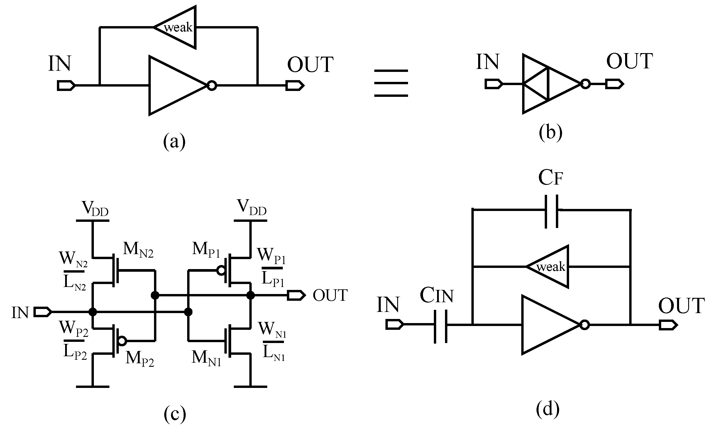
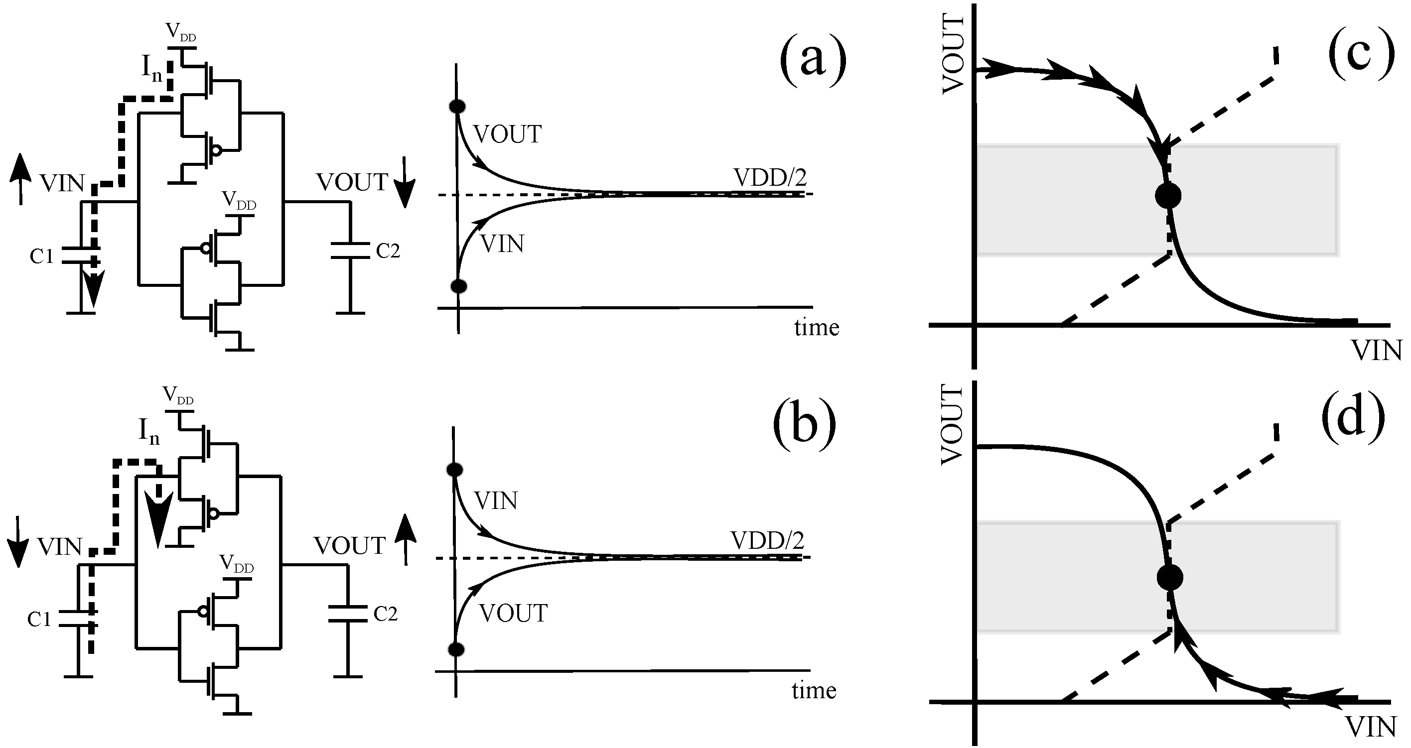
The structure of a Pseudo Floating gate amplifier is represented in
Figure 1.
Figure 1a represents a PFGA at system level,
Figure 1b shows the symbol adopted in literature to represent this type of amplifier and
Figure 1c shows the amplifier at transistor level.
The amplifier is made of four transistors, two to implement a logic inverter (
,
) and the other two to implement a voltage buffer (
,
). The voltage buffer provides the biasing for the inverter, which is forced to work as an amplifier rather than a digital logic device. The system is brought into the equilibrium state by the current leakages of the buffer, which is turned off during the whole operation of this device. Such buffer is usually denoted as “weak”, because it does not give any contribution to the amplifier, except for the weakly biasing of the inverter. Therefore, the PFGA inherits most of the characteristics of the inverter. In order to work properly, the input signal has to be connected to the PFGA through an input capacitance
as shown in
Figure 1d, otherwise the voltage buffer cannot provide the correct biasing voltage for the inverter. In [
30] it has also been proved that by adding a feedback capacitor, it is possible to control the gain of the amplifier (
Figure 1d). Ideally, the equilibrium state is reached when
, because it corresponds to the equilibrium point of a PFGA made of an ideal inverter and an ideal voltage buffer as shown in
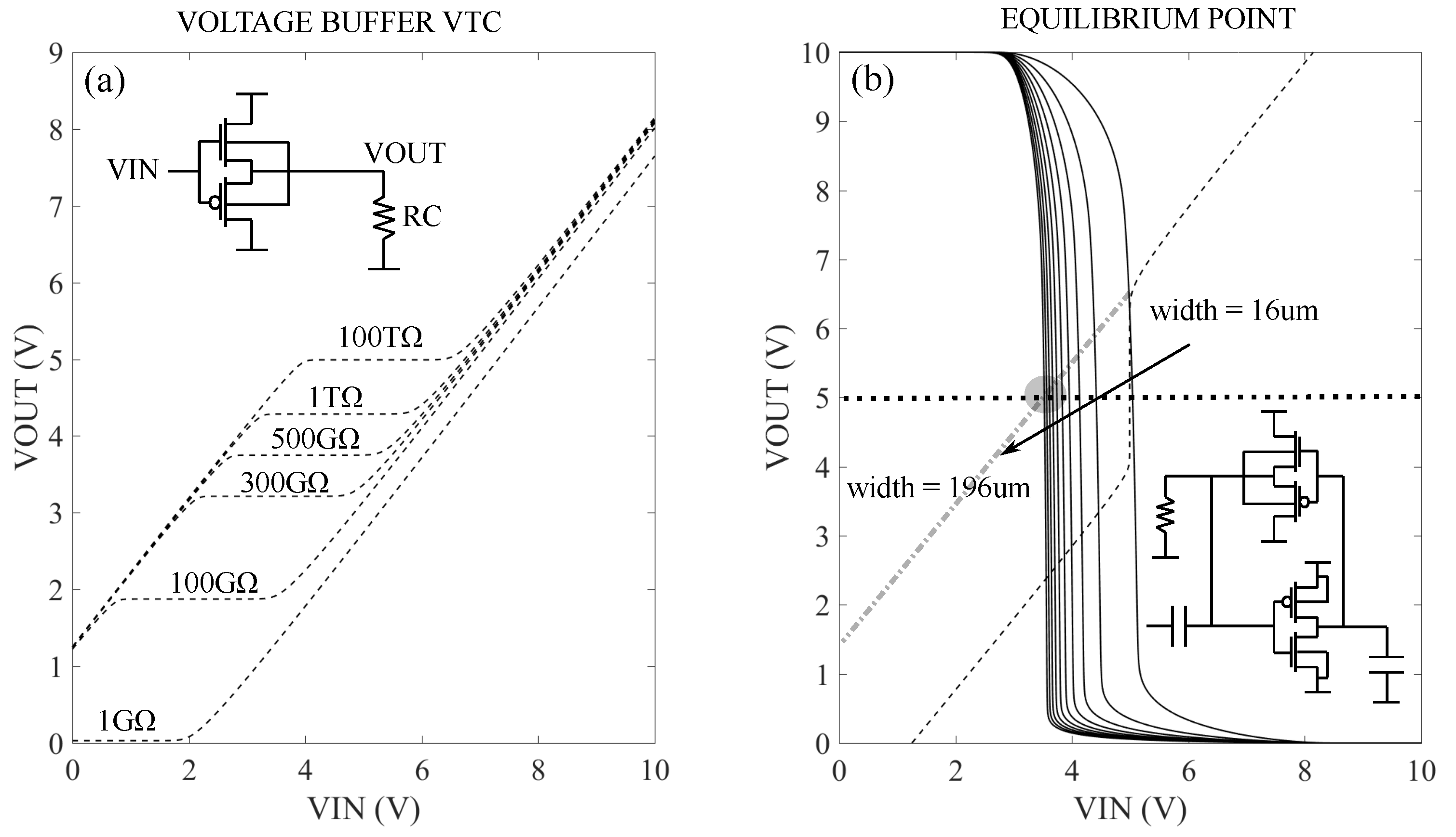
Figure 2a–c.
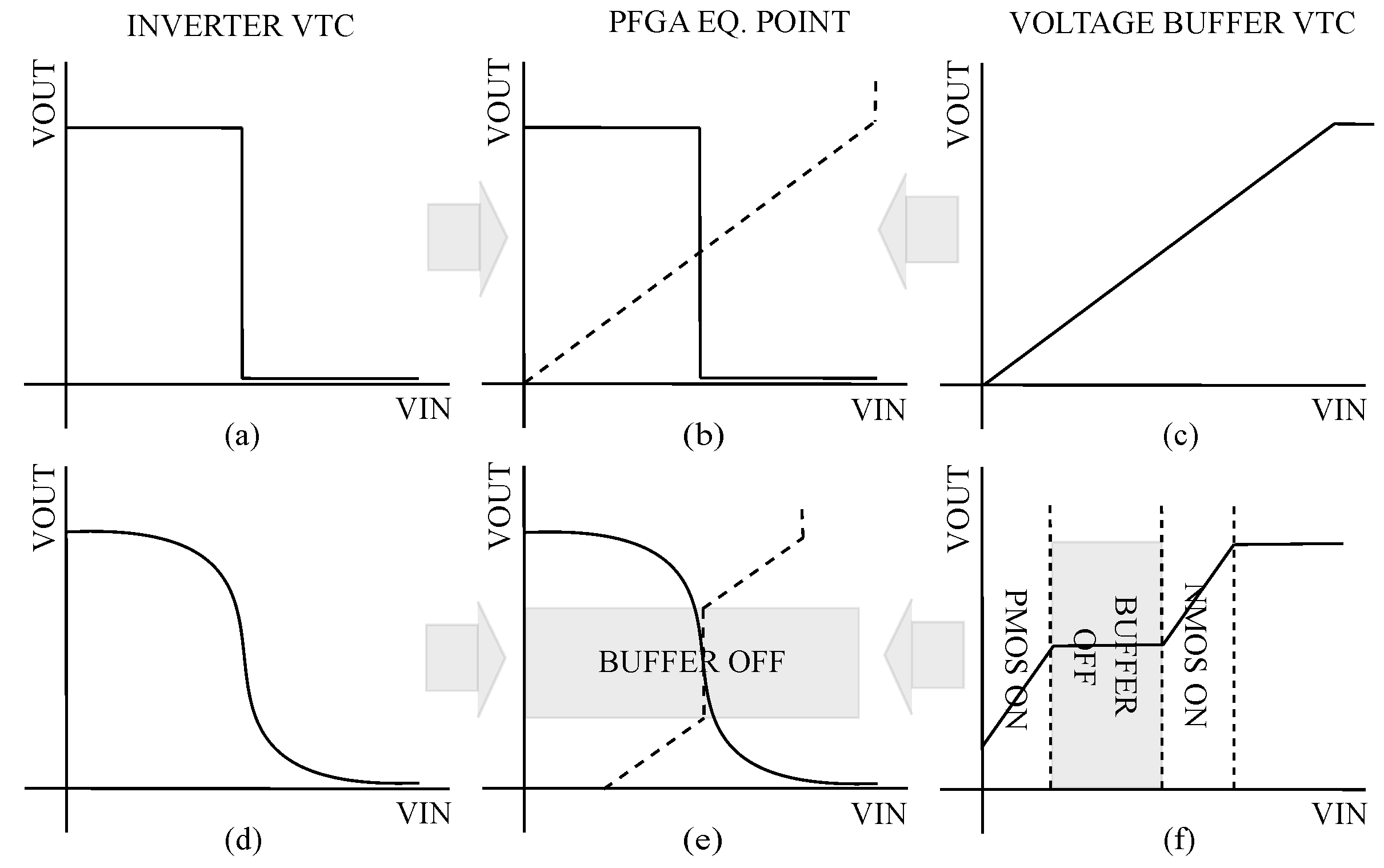
Figure 2a–c shows a graphical representation of the equilibrium point defined by the intersection of the ideal voltage transfer characteristic (VTC) curves of these two devices. A more realistic representation, which considers the transistor implementation of the PFGA, is shown in
Figure 2d–f.
Figure 3 shows two different approaches to understand and visualize the working principle of this amplifier. The first one is from a dynamic point of view, while the second one is from a static point of view.
Figure 3a,b shows a transient analysis of two different situations, in which the input and the output start from two opposite initial conditions, and then the system is left by itself to bring back the equilibrium. These graphs show that after a finite amount of time, the voltage at the input and output node approach the same value due to the feedback reaction of the NMOS (N-type MOSFET) or the PMOS (P-type MOSFET) in the voltage buffer.
Figure 3c,d shows the same situations, assuming that the working point is moving over the voltage transfer characteristic curve (VTC) of the inverter, which occurs when the input node is much slower than the output node. The static analysis in
Figure 3c,d shows more clearly how the working point is at first driven by the NMOS or PMOS in strong inversion and then, since the buffer turns off (grey region), only the channel leakage currents of the same MOSFET could finish bringing this amplifier in the equilibrium state. It is now clear that this amplifier is meant to be fabricated with high leakage CMOS processes, therefore a low leakage implementation could introduce some design issues to take into account. In particular, the dominant contribution to the leakages considered in this paper is the subthreshold channel currents of the MOSFET in the voltage buffer. In the next sections, we will investigate how to implement the PFGA in low leakage CMOS technologies.
3. Low Leakage PFGA Requirements
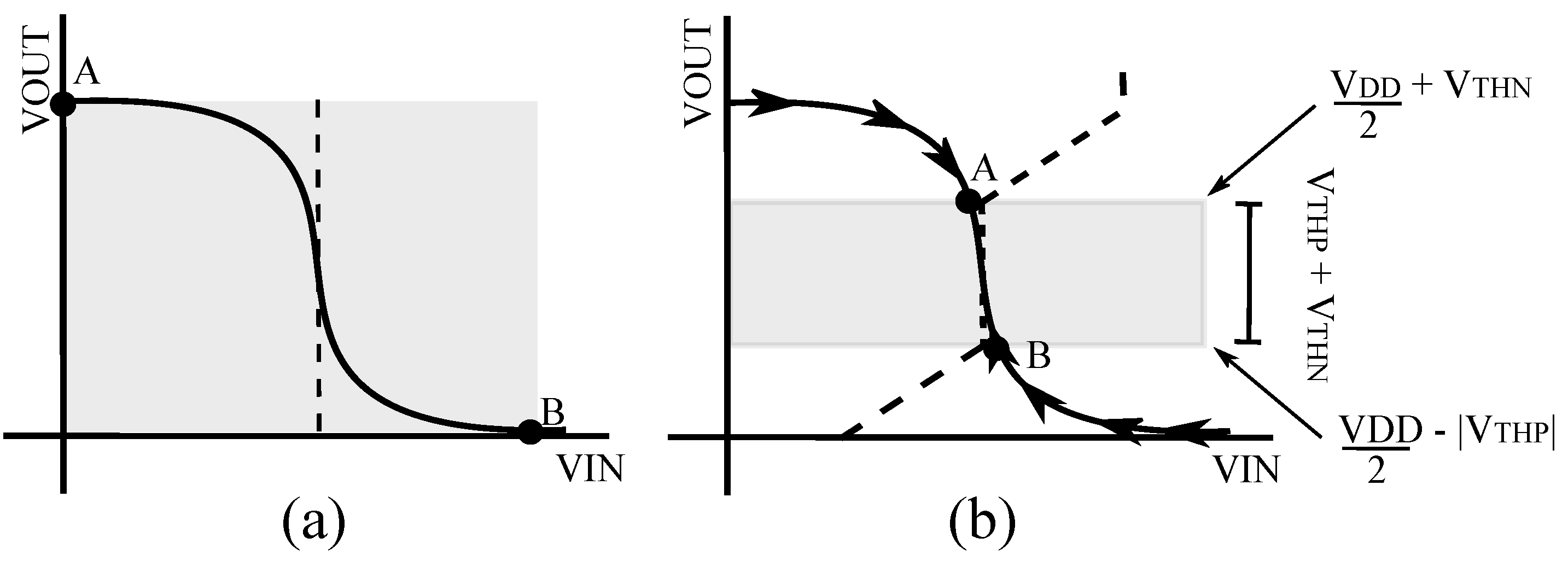
Before starting the analysis of a low leakage PFGA (LL-PFGA), the requirements to design this amplifier must be investigated. Therefore, two cases are considered: one in which the voltage buffer is turned off for any value of the input voltage and the other one in which the voltage buffer is turned off in a limited range of the output swing. These two situations are represented in
Figure 4a,b respectively.
Figure 4a represents the ideal behaviour of a PFGA in high leakage technologies where the voltage buffer provides the only biasing of the inverter by means of the leakage currents. Nevertheless, in the case of a very low channel leakage, the sub-threshold currents of the voltage buffer needs a long time to bring the input node of the PFGA to the equilibrium point. The approaching time to this point could be so long, that the output and the input voltage seem to remain fixed to one of the rail of the power supply (points A and B
Figure 4a), even if they are moving very slowly toward
. This situation can occur when high floating gate capacitances and low values for the power supply are used in addition to low leakage transistors, to implement the amplifier.
Figure 4b shows that one of the transistors in the voltage buffer is ON until the input voltage reaches a value around the equilibrium, then it turns off. This situation is the typical case of a normal PFGA design characterized by high channel leakage, which does not introduce any problems. In this case, the working point continues to move due to the sub-threshold currents in opposite to a low leakage PFGA. From the biasing point of view, it seems that the smaller is the OFF range of the voltage buffer, the better is the position of amplifier working point. However, this design strategy has two side effects. The first one is that the biasing is mainly due to the voltage buffer in ON state, which increases the power dissipation of the amplifier. The second is that the smaller the OFF region of the voltage buffer, the smaller is the output swing of the amplifier. Indeed, this range is defined as the interval of output values in which the inverter works as an amplifier and the voltage buffer is turned off. Therefore, to maximize the output swing, the off region of the voltage buffer must be larger than or equal to the range in which the inverter works as an amplifier. Finally, it must be noticed that the OFF region of a CMOS voltage buffer is not easily controllable. Indeed, the width of the OFF region of an unloaded voltage buffer (
) depends on the threshold voltage of its MOSFET, as shown in
Figure 4b. This parameter is not easy to control unless a triple well process is used to implement a bulk driven technique, which increases the cost of this device. In order to avoid to fall in the case shown in
Figure 4a, it is necessary that
. If this condition is not met, the bias point remains fixed in a position far apart from the ideal value. It is also interesting to notice that this condition does not allow to design the inverter in the PFGA in weak inversion. Although increasing the power supply seems like a good method to consider the OFF region of the voltage buffer smaller than the available output swing, it must be taking into account the body effect of the transistors in the voltage buffer, which increases their threshold voltages and therefore the OFF region. In conclusion, in this section the main difference between LL-PFGA (Low leakage PFGA) and HL-PFGA (High leakage PFGA) has been exploited, which consists in the transient time to approach the equilibrium point. Furthermore, an analytical condition of the power supply has been provided to allow the design of a LL-PFGA.
4. Offset in a Low Leakage PFGA
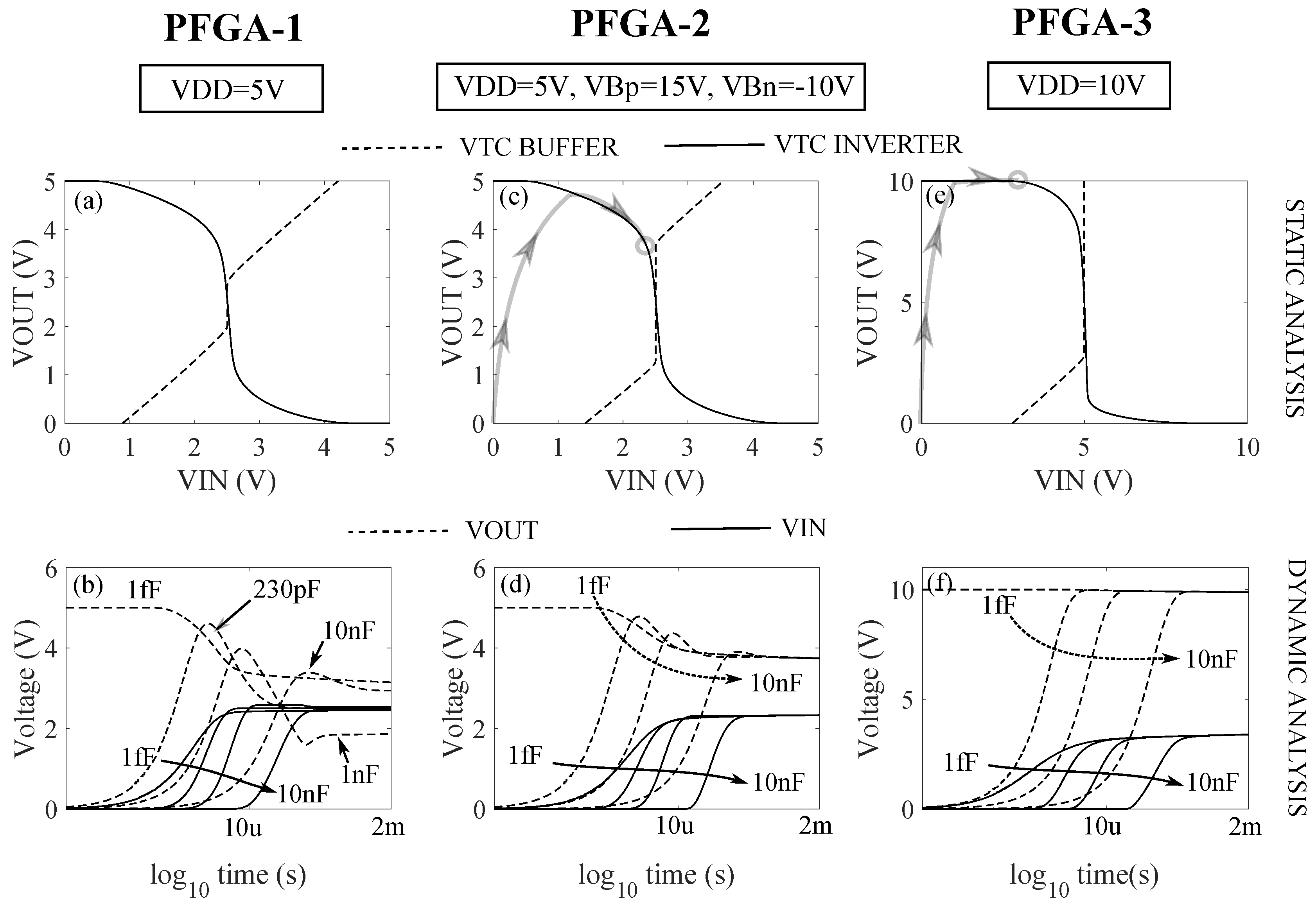
The first step in the design of a LL-PFGA is the dynamic and static analysis of the circuit, which are used to determine the position of the bias point. In this work, these analyses are performed for
V, 10 V. The AMS-350nm technology provides many types of different models but only the nmos4/pmos4, nmos20h/pmos20h are suitable to implement a LL-PFGA in this range of voltages. The threshold voltages for these models are shown in
Table 1.
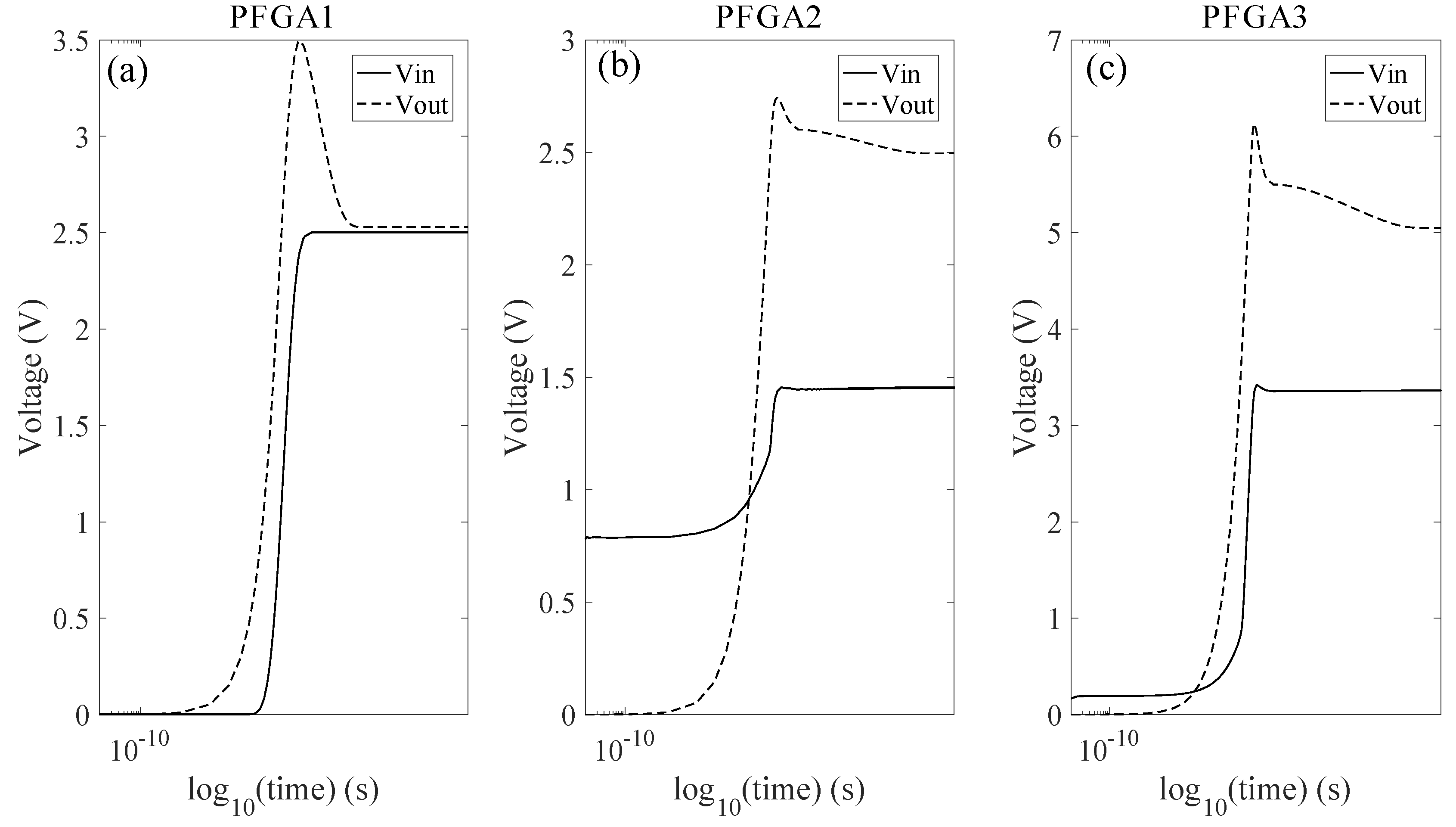
By using these models, three scenarios have been investigated : PFGA1 with nmos4/pmos4 at
V, PFGA2 with nmos4/pmos4 at
V and body terminal connected to
V,
V and PFGA3 with nmos20h/pmos20h at
V. The connections of the PFGA2 body terminals allow to mimic the behaviour of a PFGA with a wider OFF region of the voltage buffer. These three cases are represetned in
Figure 5.
All of the three cases represented in
Figure 5 describe low leakage PFGA, since the bias point cannot approach the ideal equilibrium point.
Figure 5b,d,f show that after the power supply is connected to the amplifier, the values of the input and the output voltage start to rise. In particular, the output voltage grows faster than the input voltage because at the beginning of the initial transient
V. Therefore at
the PMOS of the inverter is completely turned ON, while both MOSFET in the voltage buffer are still turned OFF. After, the output voltage reaches a certain value at which
the NMOS of the voltage buffer turns ON and the input node voltage starts to rise. Finally, the two signals try to converge to the equilibrium point. The two cases shown in
Figure 5d,f present the behaviour expected from the static analysis in
Figure 5c,e. The trajectory of the working point is represented in grey line with arrows in
Figure 5c,e. For the case in
Figure 5c,d, the working point moves toward the ideal equilibrium point until the voltage buffer turns off (flat region of the VTC of the voltage buffer), which stops it. The static analysis of the PFGA3 shows that the OFF region of the voltage buffer is larger than the expected value (
). This is because in this technology, the threshold voltage is highly affected by the body effect, thus increasing significantly the OFF region of the voltage buffer. For the case in
Figure 5e,f, the working point is almost fixed at one rail of the power supply, since the buffer is always OFF and the leakages are not strong enough to move the bias point toward the ideal value. In the three cases of study, it has been tested if the dynamic of the system is affected by the time constant of the input and the output node. This test has been performed by varying the values of the load capacitance. The dynamic of the PFGA2 and the PFGA3 seems to be independent from any variations of the load capacitance, rather than the dynamic of the PFGA1 in
Figure 5a,b. In particular, there exists a situation (
pF,
pF) which is highly favorable to the biasing of PFGA1. For these particular values of input and load capacitances, the bias point approaches very close to the ideal value. It has been concluded that when the OFF region of the voltage buffer is relatively narrow to place the bias point in the linear region of the inverter, the trajectory of the working point is controlled by the values of the time constants of the input and the output node of the PFGA. This is because the inverter is highly sensitive to input voltage variations which occurs in its linear region. While, if the buffer turns off when the bias point is at the edge or outside the linear region, then the dynamic is controlled by the static characteristic of the PFGA and the trajectory of the bias point can be predicted by the graphical representation of the VTC curves as done for the cases in
Figure 5c,d,e,f. These are three possible scenarios that can occur when a low leakage PFGA is designed. For the PFGA1, the position of the bias point can be optimized by selecting a precise value of the input coupling capacitance
, which is usually in the same order of the load capacitance. For the other two cases, it is necessary to wait an unreasonable amount of time before the working point reaches the ideal equilibrium state. In this paper, the distance between the point A or B shown in
Figure 4b from the ideal bias point (
) will be referred to as “offset” of the amplifier. In particular,
will be referred to as input offset and
will be referred to as output offset of the LL-PFGA. In order to provide a properly working LL-PFGA, this offset must be compensated by using other techniques, which will be described in a later part of this work. All of these three PFGA will be analyzed and designed in order to provide the correct bias point and a working amplifier.
5. Offset Compensation Techniques for Low Leakage PFGA
In the previous section, three possible PFGA designs have been analyzed. These cases will be referred as PFGA1 (
Figure 5a,b), PFGA2 (
Figure 5c,d) and PFGA3 (
Figure 5e,f). The offset of the PFGA1 can be compensated by tuning the input capacitance to a value in the same order of the output capacitance value. Therefore, once the value of the load capacitance is known, it is possible to compensate easily the offset for the PFGA1. The PFGA3, PFGA4 cannot be used as amplifiers since their bias point is too far from the ideal value. This section provides design rules to compensate the equivalent offset for PFGA2 and PFGA3. These design strategies can be implemented without using any other electronic circuit, but they are based on the optimization of the basic structure of the PFGA and by adding only one resistor in the circuit. There are two main problems in PFGA2 and PFGA3 : the first one is that the bias point, although looks constant, is continuing to move toward the ideal equilibrium point very slowly, moved by the low magnitude of the leakage currents of the voltage buffer. The second problem is that the bias point is still very far from the ideal value (
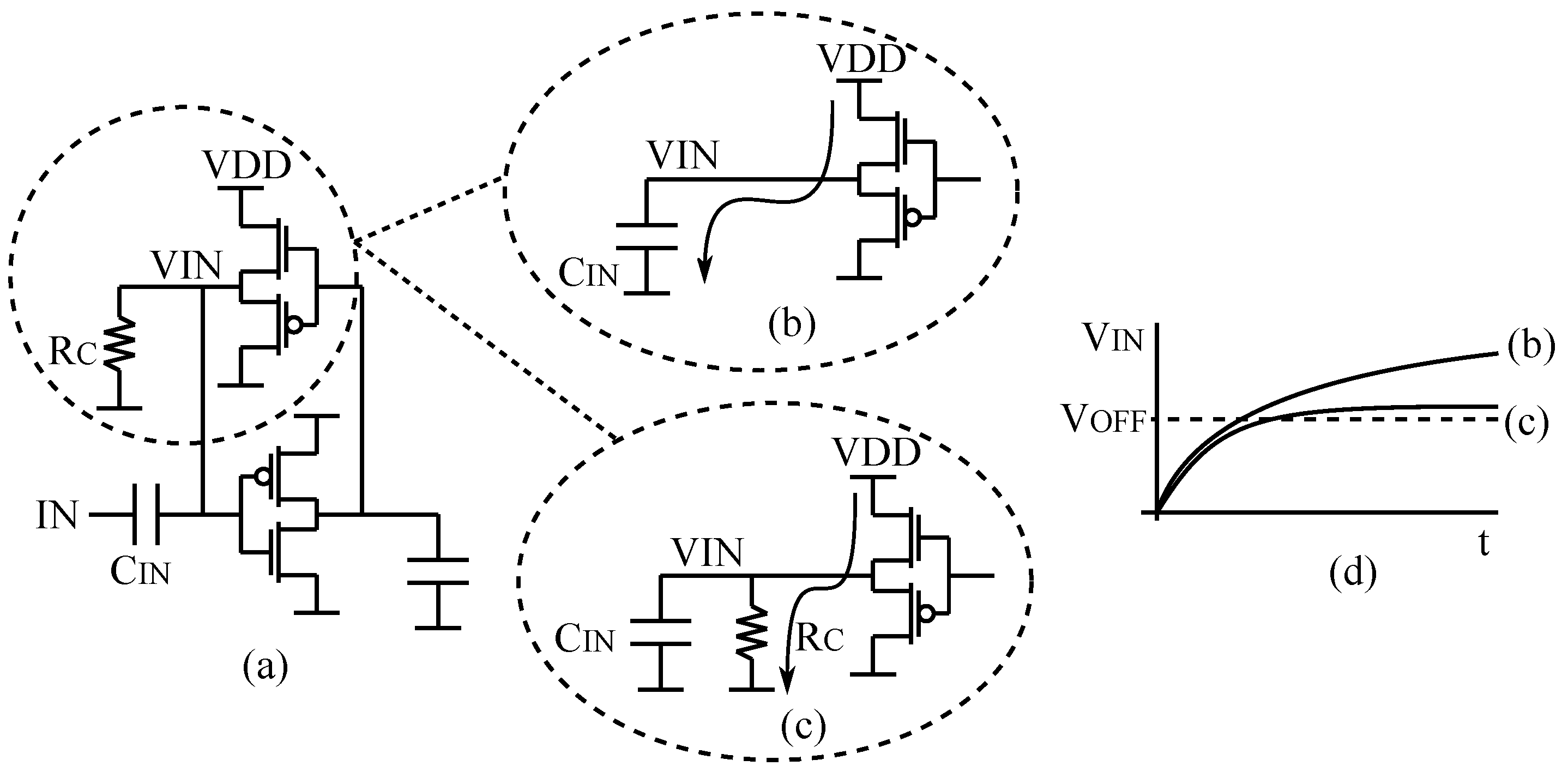
). The fact that the bias point is continuously moving after the voltage buffer turns off, means that after a very long time, the bias point could be different and so the PFGA characteristics can also change in time. The first problem can be addressed by adding a resistor at the input node of the PFGA as shown in
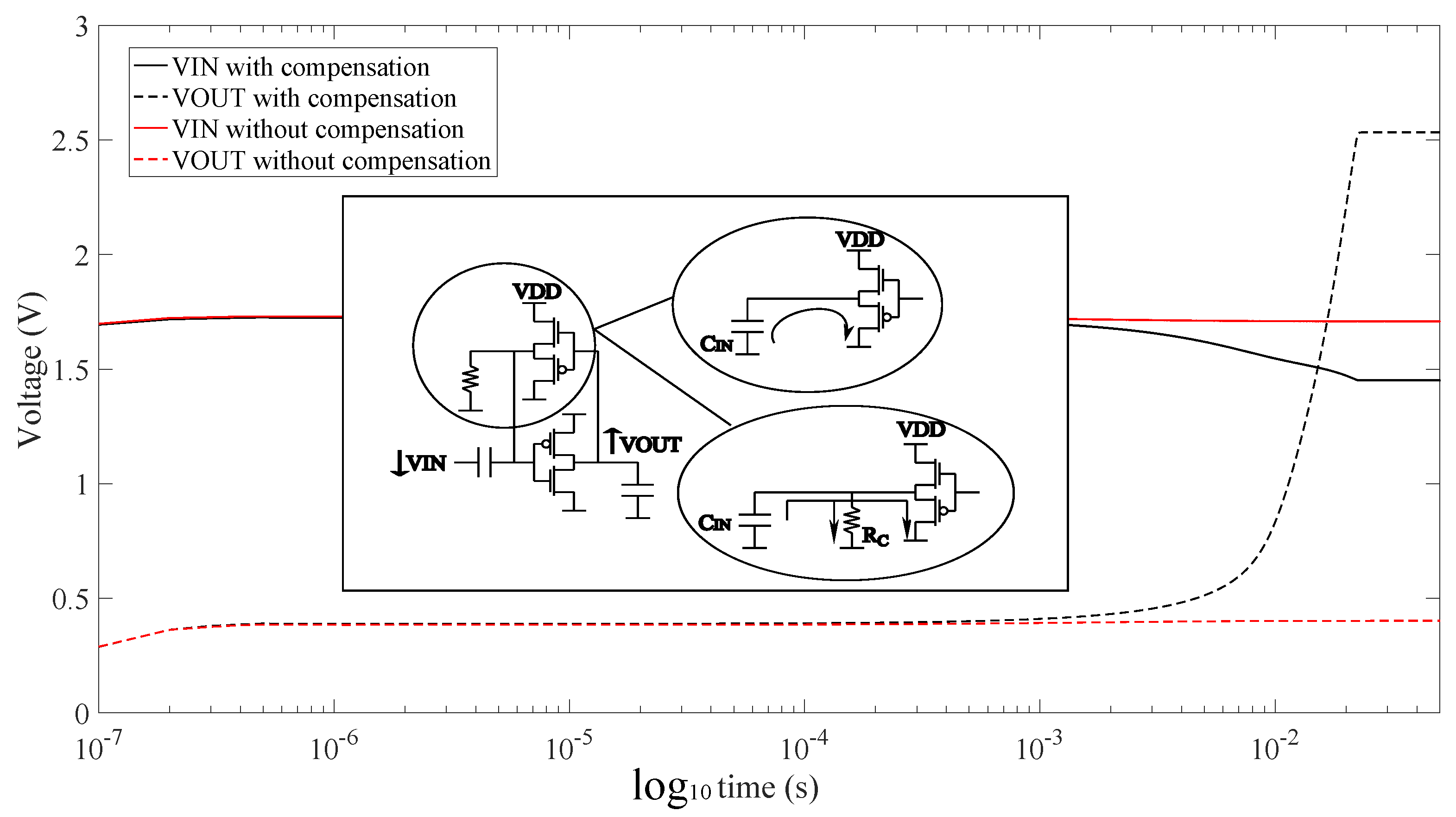
Figure 6a.
Figure 5d shows that the bias point continues to move after the voltage buffer turns OFF because the input node is charged by the leakage currents of the voltage buffer as shown in
Figure 6b. The resistor
is used to create a path for the leakage current generated by the voltage buffer in order to stop the charging of the
when
, as shown in
Figure 6c.
Figure 6d shows the comparison of the signal
for a PFGA with and without
. By using
, the working point becomes stable at a precise value and it is easy to implement in CMOS technology with a voltage controlled MOSFET. Unfortunately, this advantage occurs at the expenses of the position of the bias point, which moves further from the ideal state as the
value decreases. This phenomenon is exploited in a graphical representation showed in
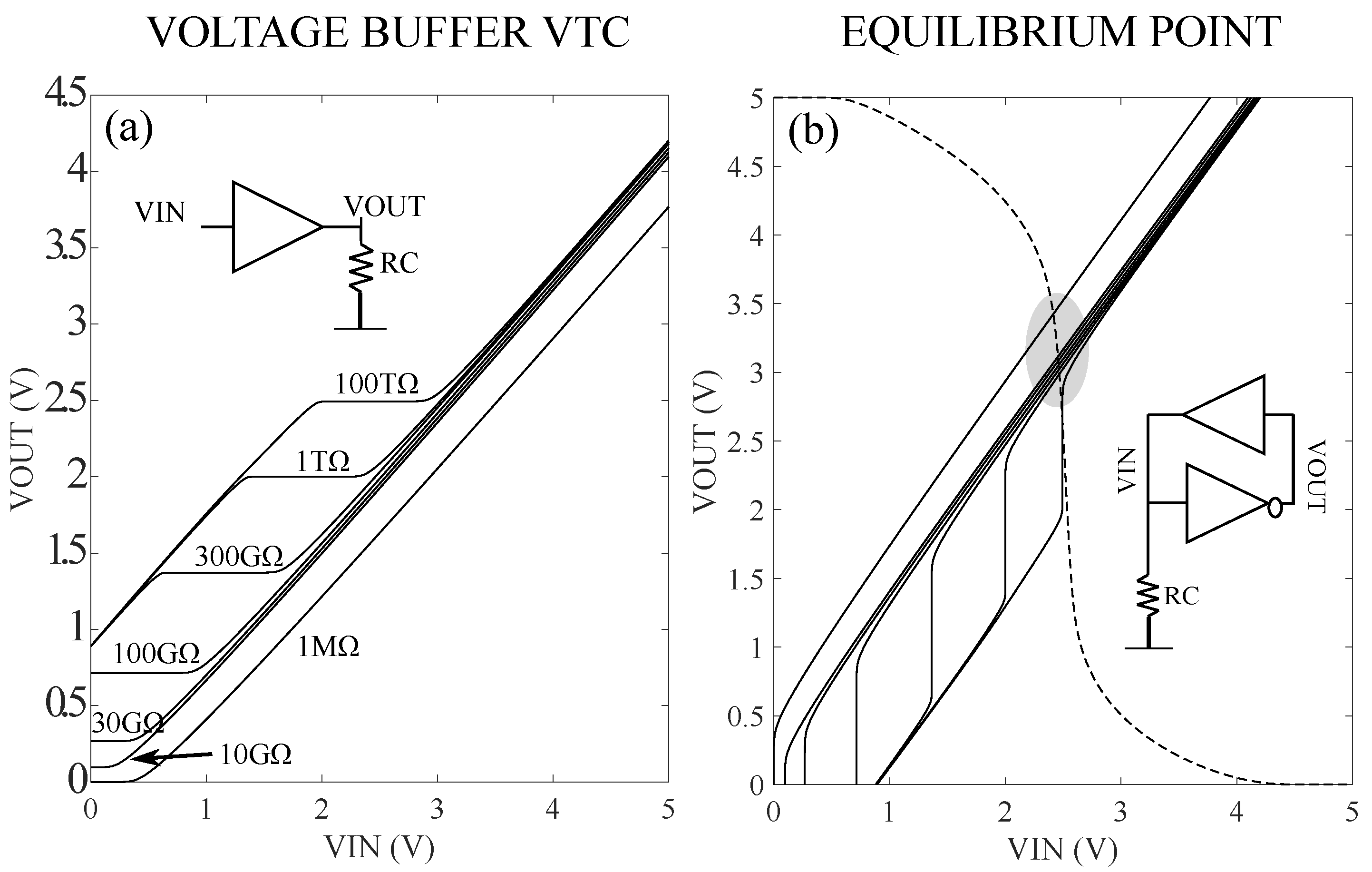
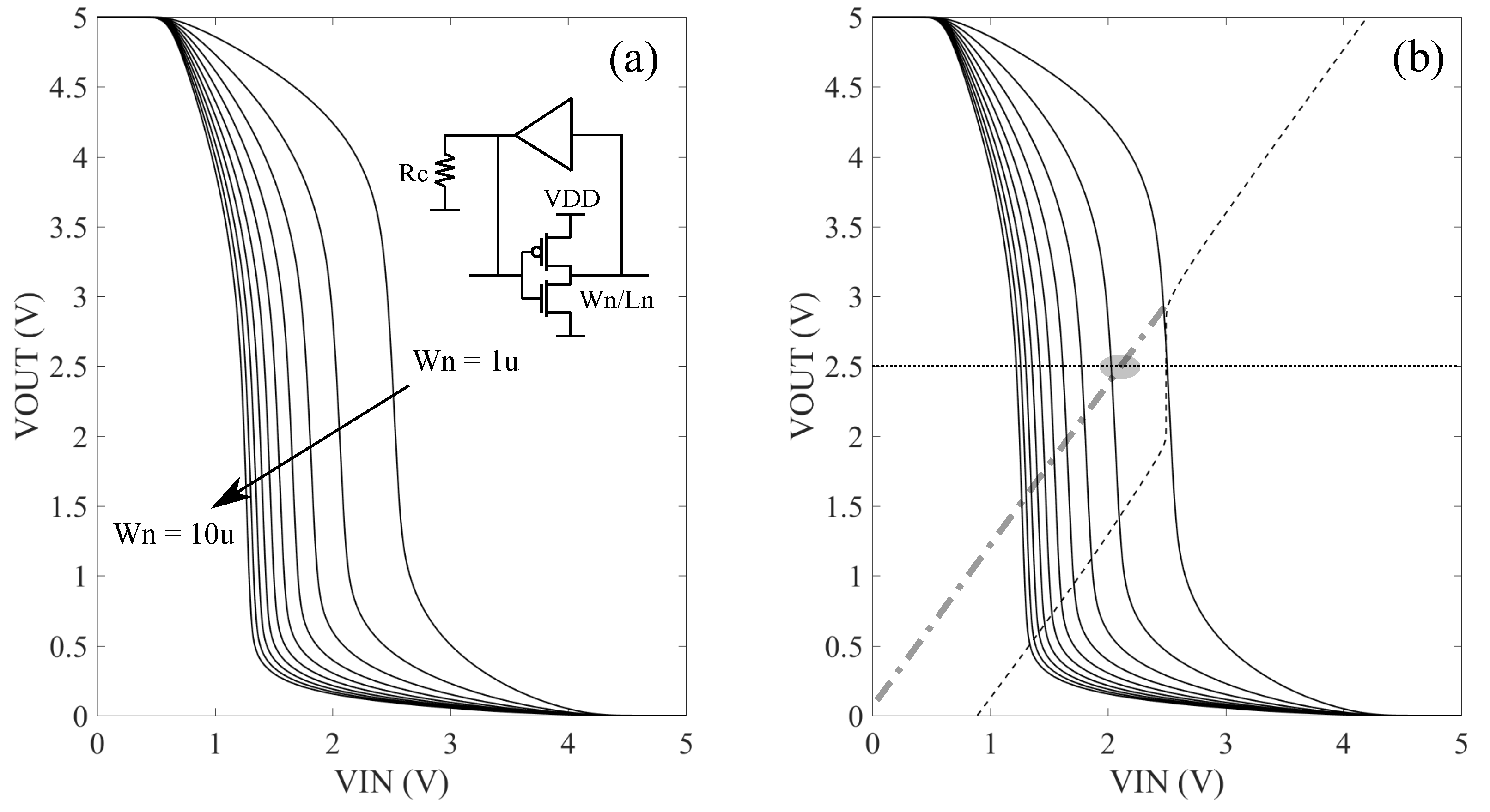
Figure 7.
Figure 7a shows how the VTC of the voltage buffer is dependent on the resistance value
.
Figure 7b shows that by reducing the value of the compensation resistor
the bias point moves further from the ideal value. Therefore, the value of this resistor has to be maximized in order to provide a negligible effect to the position of the bias point, but low enough to absorb the current of the NMOS of the voltage buffer. Furthermore, the
must be higher possible to keep in weak inversion the NMOS inside the voltage buffer and the NMOS used to implement the resistor, minimizing the power consumption of the circuit.
The second problem to solve consists in moving the bias point closer to the ideal value. In the previous section, this point has been always recognized as
, because it corresponds to the equilibrium state between an ideal inverter and an ideal voltage buffer. However, in order to maximize the output swing of the amplifier, it is sufficient to provide
, point at at which the gain is maximized.
Figure 8 shows a simple strategy to move the output voltage toward
.
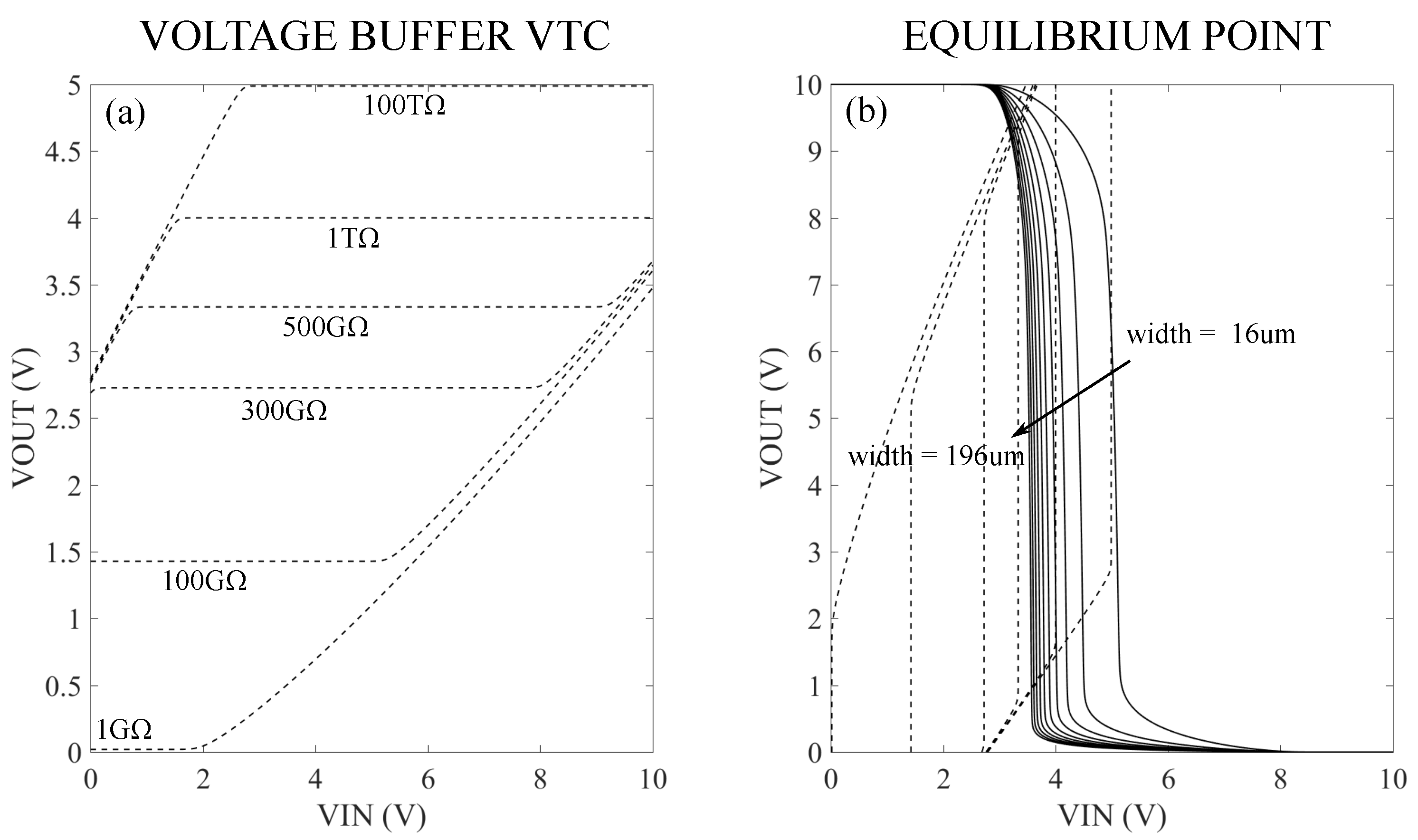
This task is accomplished by lowering the transition region of the inverter VTC curve as shown in
Figure 8a.
Figure 8b shows the new position of the bias point (circled in grey). This point is represented in
Figure 8b by the intersection of the VTC curve of the inverter and the extension of the VTC curve of the voltage buffer (dashed-dotted line). The simplest method to lower the transition region of the inverter VTC, consists in designing a very strong NMOS and a very weak PMOS. Therefore by maximizing the aspect ratio of the NMOS and minimizing the aspect ratio of the PMOS, the transition region can be lowered, moving the bias point toward the center of the output range. The optimum value of
depends on the threshold voltage of the NMOS, which determines the region in which the buffer is turned off. The higher is
, the higher will be the NMOS aspect ratio necessary to fix the bias point to the correct value. Unfortunately, the efficiency of this technique is limited, since the increasing size of the inverter NMOS produces smaller variations in the inverter VTC curve as shown in
Figure 8a.
It must be noticed that the methods proposed work also when the negative feedback is driven by the PMOS in the voltage buffer. This event occurs every time the feedback reaction of the PFGA starts from a point where
and
V. Where :
is the input value at which
. The worst case of
V is simulated in
Figure 9.
In this scenario, the
resistor does not compensate the current of the PMOS during the feedback reaction. However, it contributes to decreasing the input node voltage before and after the voltage buffer turns off, until
, at which the NMOS of the voltage buffer turns on and the dynamic of the system falls in the case previously described.
Figure 9 compares the cases with and without
. For the case without
, the PFGA cannot reach the output voltage and it remains close to the lower power supply rail value. In conclusion, by using
and moving the linear region of the inverter to a lower input voltage range, it is possible to compensate the offset for the PFGA1 and PFGA2.
The PFGA3 represents the worst case of PFGA design. The techniques previously explained are not suitable anymore as shown in
Figure 10.
It can be observed that the off region of the voltage buffer extends until the positive power supply rail. This characteristic is good for high leakage CMOS PFGA since it removes any effect of the voltage buffer to the input node, but it is a side effect in low leakage PFGA, because it moves the bias point at the maximum distance from the ideal value. In this case even an inverter characterized by a VTC curve with low value of
cannot fix the biasing problem. It can be proved that the main reason of the very large OFF region is due to the body effect. A possible way to overcome this problem consists in connecting the body terminal of the transistors in the voltage buffer to the source terminal as shown in
Figure 11.
This method completely removes the body effect of the transistors in the voltage buffer, reducing the range of its OFF region. After connecting the body to the source terminal for the NMOS and the PMOS of the voltage buffer, it is possible to use the previous two techniques to adjust the bias point of the PFGA. This approach is not suitable for N-WELL CMOS processes, which do not allow these connections, but it can be used for all the other processes, that provide bulk terminals for each single MOSFET in the IC. Furthermore, it can be applied for power MOSFET and discrete MOSFET, in which the body terminal is already connected to the source during the fabrication process. Unfortunately, this method introduces also a risk of latch-up phenomena since the body terminals are not connected anymore to the highest and the lowest electrical potential in the circuit. This risk can be minimized if the amplitude of the input signal is kept in a limited range. Finally, the effects of the design methods previously discussed are represented in
Figure 12. The Parameters used for these simulations are collected in
Table 2.
Figure 12, shows that the output node voltage after the initial transient approaches the middle value of the output range. The bias point for the PFGA2 and PFGA3 has been stabilized by using a MOSFET
which realizes the resistor
. The bias point of the PFGA1 instead, has been adjusted by using
pF when the amplifier is loaded by a capacitance of 100 pF.
In conclusion, methods have been discussed to compensate the offset in low leakage PFGA without altering the structure of the PFGA and it has been emphasized the important role of the body effect for the low leakage processes.
6. Non-Linearities in PFGA
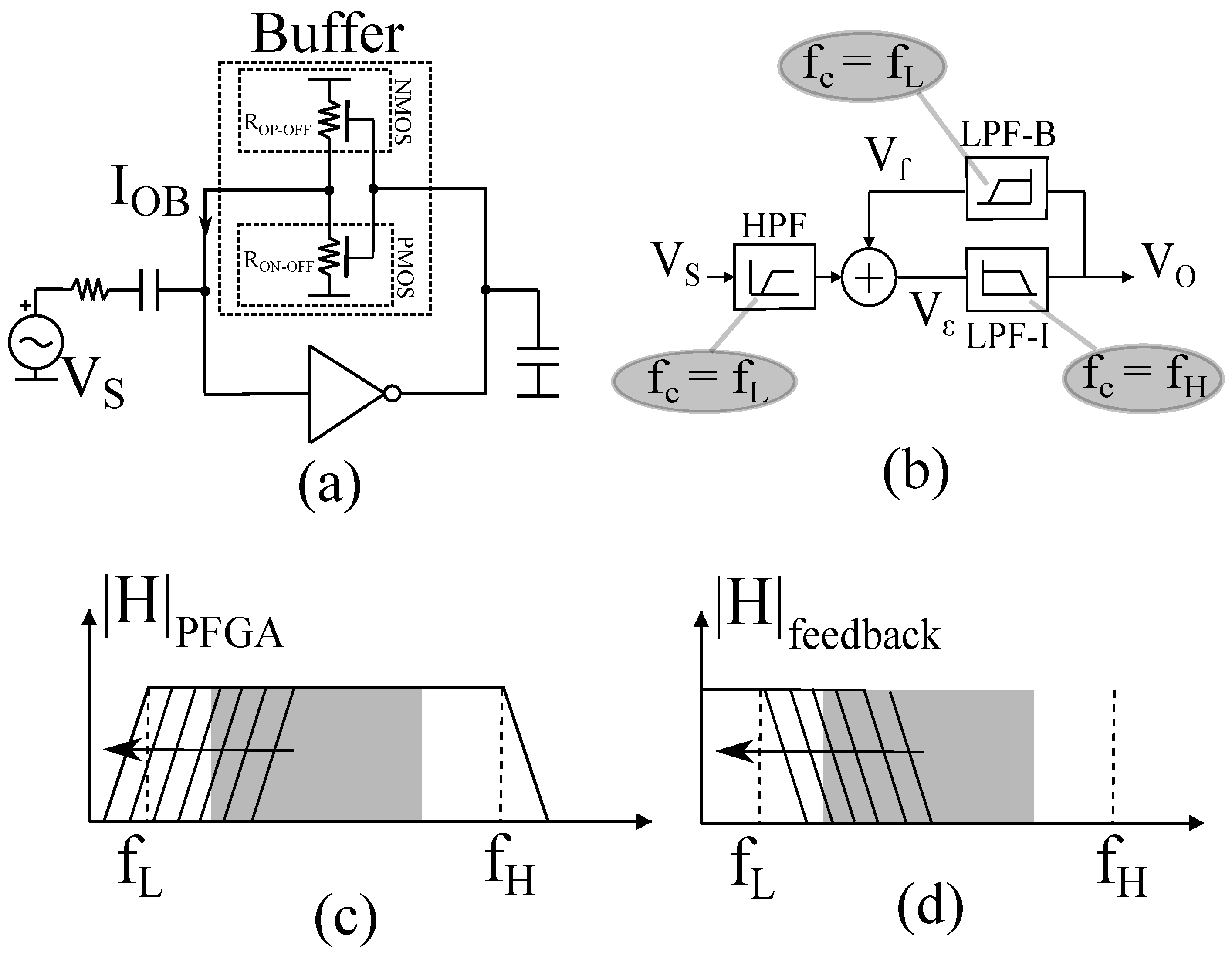
An important parameter which characterizes an amplifier is the linearity. The origin of the non linear behaviour in a low leakage or in a high leakage PFGA is the same and it is due to the effects of the signal brought back at the input node by the feedback of the PFGA. Indeed, the relation between the output current and the input voltage of the buffer is highly non linear, because the wide amplitude of the output signal of the PFGA. Fortunately, the structure of the PFGA realizes a system, which automatically filter out the effects of the feedback signal and minimizes the non linearities due to the current generated by the voltage buffer. The idea behind this concept can be represented by using the large signal model of the amplifier, shown in
Figure 13a.
The voltage buffer can be modelled by two controlled resistors, which with
create a low pass filter for the output signal of the voltage buffer. On the other hand, the same components realize a high pass filter for the source signal
. Finally, the inverter adds a low pass filter behaviour to the PFGA frequency response. The system can therefore be represented with a block diagram as shown in
Figure 13b. Since the input high pass filter and the low pass filter on the feedback are made by the same components, they also present the same cut-off frequency (
), which corresponds also to the low cut-off frequency (
) of the PFGA. The signal
is made by two contributions: the filtered input signal
and the feedback
. Since the non linearities are caused by
, then it is possible to reduce the distortion of the PFGA by lowering the cut-off frequency of the LPF on the feedback path. If the cut-off frequency of the LPF on the feedback is low enough, then the output buffer current is filtered out, giving no contribution to the input voltage of the PFGA, thus minimizing the distortion. This technique guarantees that the feedback signal is removed inside the range of frequencies utilized by the input signal (
). The easiest way to control
is by tuning
. The effectiveness of this technique is shown in
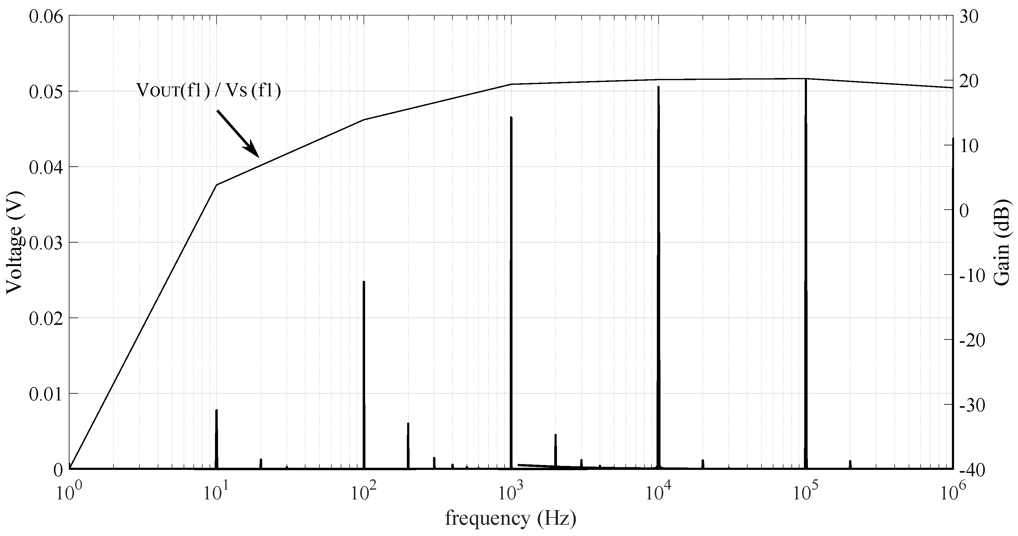
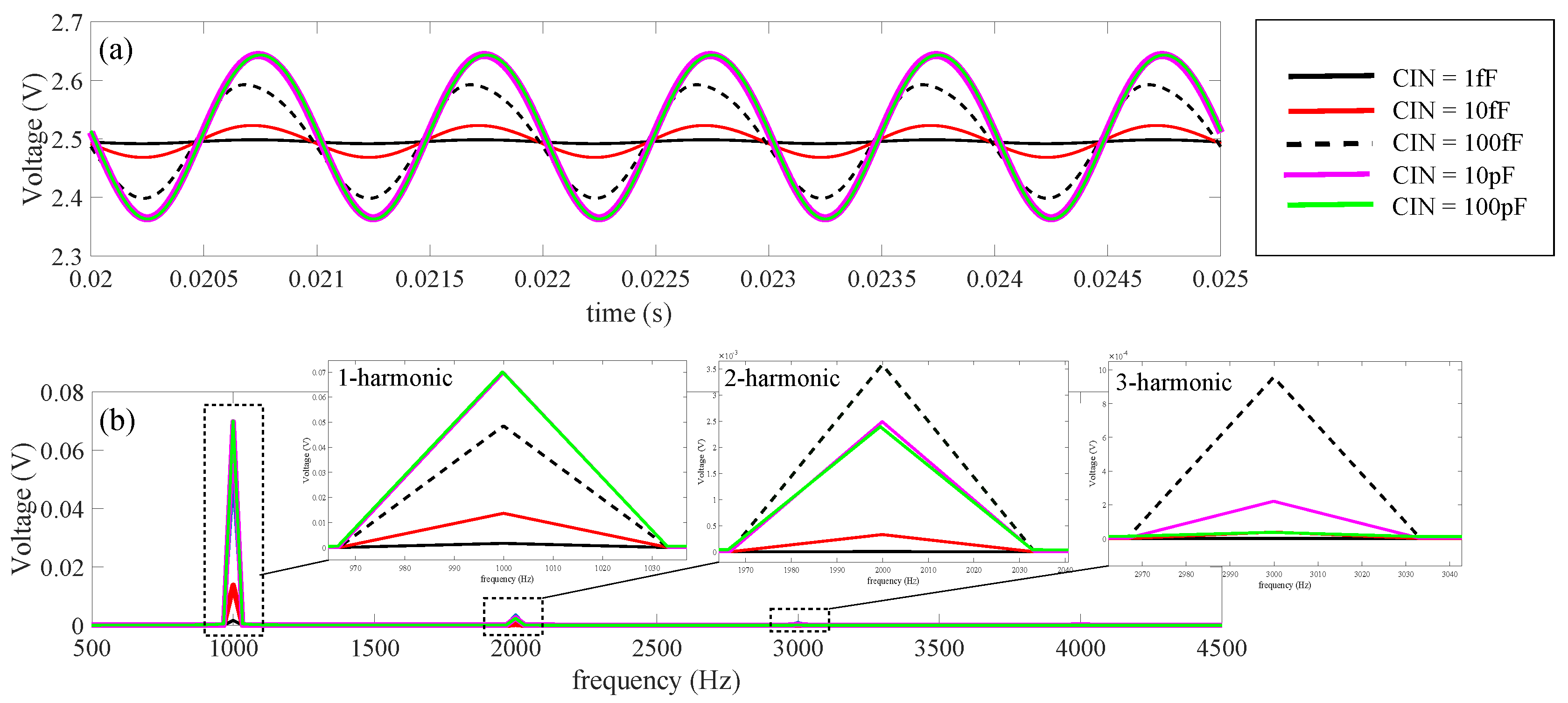
Figure 14, which represents a simulation in AMS-350nm for the PFGA2.
It must be pointed out that thank to the compensation of the offset, the bias point now lays in the linear region of the inverter and variations in the value of
can affect the dynamic of the PFGA, as previously discussed for the PFGA1. Therefore, during the sweep of the
the bias voltage of the equivalent resistor
has been adjusted to keep the average value of the output signal at
.
Figure 14 shows the simulation results for a sweep in the value of
after that the frequency of the sinusoidal input has been fixed at 1 kHz. The amplitude of the input signal has been set to 10 mV, minimizing the distortion due to the inverter. The non-linearities here are represented by the high order harmonic in the spectrum of the output signal. In order to evaluate quantitatively the distortion introduced by the PFGA, the total harmonic distortion (THD) parameter has been evaluated. This parameter is defined as shown in Equation (
1).
Given the low magnitude of the harmonic over the third order, this parameter has been evaluated until this frequency. Results are shown in
Table 3.
Table 3 shows that for an increasing value of
the distortion increases at first, reaching a maximum value and then decreases, approaching ideally to zero if no other sources of distortion are involved. The reason of this behaviour can be explained as follows: for low value of
, the input coupling capacitor owns a very high impedance, stopping almost completely the input signal and providing very small output for the PFGA. The small dynamic of the output signal allows to consider the buffer almost linear and the distortions introduced are negligible. However, increasing the value of
decreases its impedance, allowing a wider signal at the input node and at the output nodes of the PFGA. Thus, the larger signal at the output of the PFGA brings the buffer to introduce non linearities in the circuit. Finally, a very high value of
means very low impedance (short-circuit), which provides
and a ground path for the output buffer current. This current provides a negligible drop voltage
, which means negligible contribution of the non linearities to the input voltage of the PFGA. In conclusion, the selection of the input coupling capacitor is very important to reduce the distortion of the amplifier and set the bandwidth of the PFGA. By looking at the trend of the fundamental harmonic in
Figure 14b, it is possible to give a frequency interpretation of the same phenomenon. Indeed by increasing the value of the input capacitance, we reduce the value of the low cut-off frequency of the PFGA. The changing in the magnitude of the output voltage represents the transition from being out of band, to being inside the bandwidth of the amplifier. Since the maximum distortion happens for medium value of
, it is possible to deduce that the non linearities of the amplifier are maximized around the low cut-off frequency of the PFGA. To simply verify this hypothesis, a second simulation for the PFGA2 is performed, where the value of
is fixed to 100 fF, and the frequency of the input signal is swept in a low frequency range. The simulation results are shown in
Figure 15.
Figure 15 shows that the distortion reaches its maximum around the low cut-off frequency of the amplifier as expected. The distortion of the input and the output node signals of the PFGA, introduces a certain error in the evaluation of the low cut-off frequency because the amplitude of the input signal is corrupted in that range of frequencies. An alternative way to characterize the transfer function of this amplifier at low frequency is to consider the ratio in Equation (
2).
This transfer function is based on the ratio between the amplitude of the fundamental harmonic of and the amplitude of the source signal . This is a practical method to evaluate the trasnfer function of this amplifier, minimizing the error in the evaluation of the PFGA low cut-off frequency.
Finally, the same method can be applied for the PFGA2 and PFGA3, but not for the PFGA1 if the compensation of the offset have been realized by tuning the value of . Therefore, tuning the input capacitance to set the bias point does not allow minimizing the distortion of the PFGA and set its bandwidth.
In conclusion, the PFGA distortion can be minimized by tuning the input coupling capacitor of the PFGA, but the non linear behaviour around the low cut-off frequency cannot be removed. Finally, this section introduces an alternative definition for transfer function to remove the uncertainty introduced by the non linear distortion of the signals in the circuit.
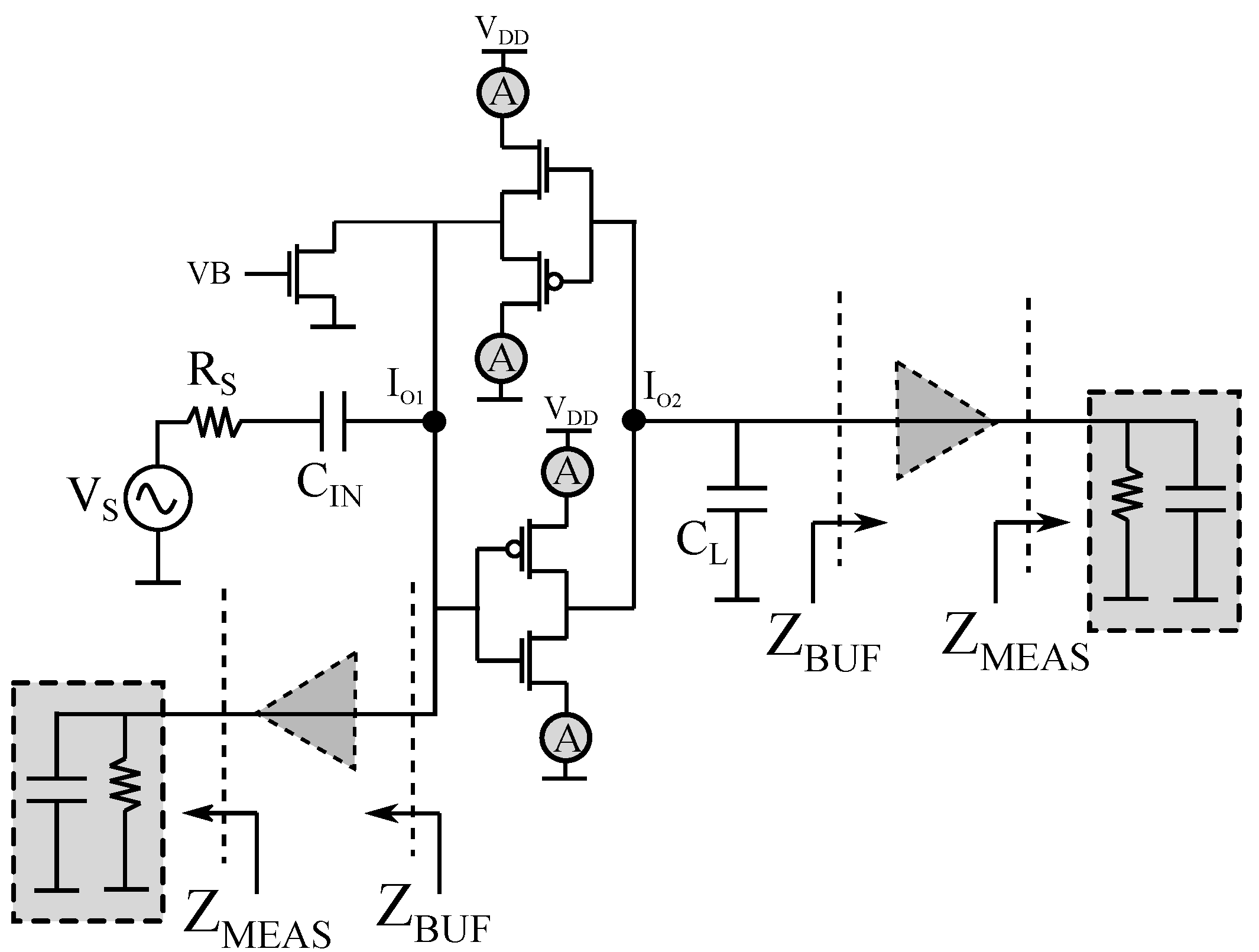
8. Measurement Set-Up
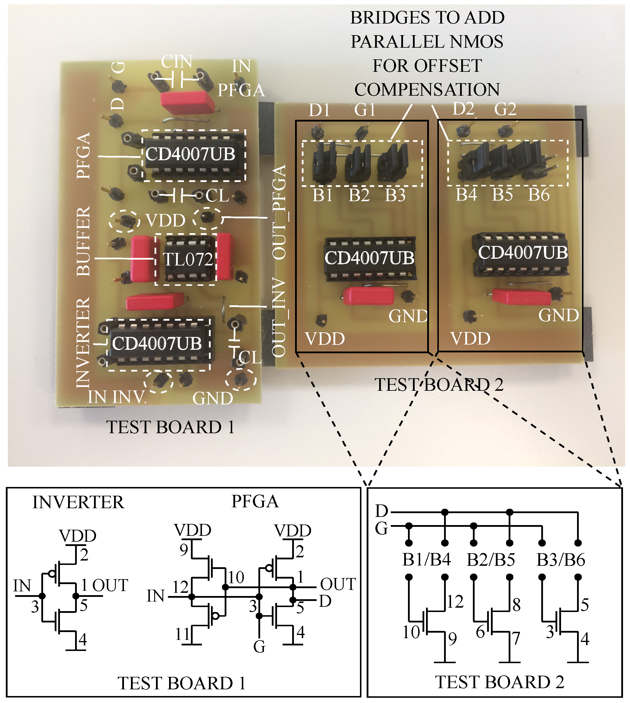
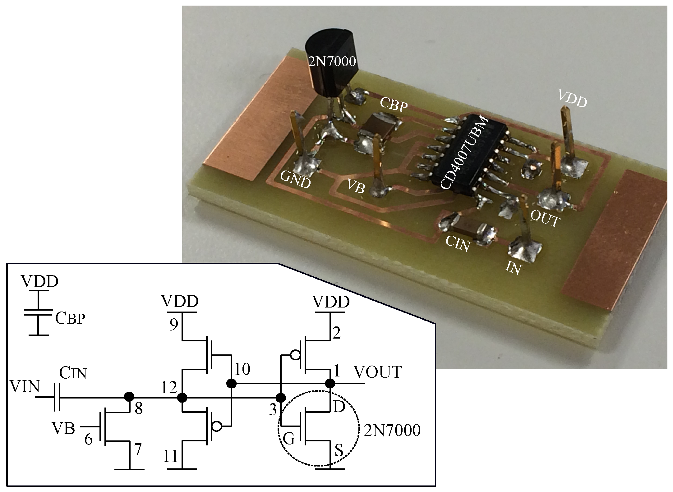
Experimental tests have been performed to validate the modelling previously discussed. A prototype has been fabricated by using discrete components and mounted on a printed circuit board (PCB), as shown in
Figure 16. The MOSFETs have been implemented by using CD4007UB (Texas Instruments, Dallas, TX, USA).
This prototype is divided in two boards. Board 1 is used to extract the analogue characteristics of the inverter and the performance of the LL-PFGA realized by using CD4007 IC. Board 2 is used to implement the offset compensation technique, providing a set of NMOS, which can be connected in parallel to the NMOS of the PFGA inverter, as shown in
Figure 16. Indeed, by placing multiple MOSFETs in parallel, it is possible to mimic the behaviour of a transistor with greater channel width. In order to connect these two boards, the terminals D and G on board 1 must be wired to the terminals D1,G1 and D2,G2 on board 2. However, the NMOS on board 2 are electrically connected to the NMOS on board 1 only after that the bridges indicated with
(where
i: 1,2,3,4,5,6), are closed. The more bridges are closed, the more NMOS are connected in parallel. The voltage controlled MOSFET
, which is used to stabilize the bias point of the LL-PFGA, can be implemented by using one of the unused transistors in the IC on Board 1 or by using another CD4007 IC. The reason why the transistors in CD4007 can realize only a LL-PFGA is because they are long channel MOSFET and they are characterized by a relatively high threshold voltage as shown in
Table 4. These two characteristics are in general sufficient to provide low leakage currents.
The parameters listed in
Table 4 have been extracted in [
31].
Measuring the voltage signal at the input node of a PFGA could affect the biasing of the amplifier, modifying the equilibrium point of this circuit. This is due to the fact that the biasing of the input node depends on the channel leakage currents of the transistor in the PFGA voltage buffer. Therefore, voltage measurements at this node require to use another voltage buffer to decouple the measuring instruments from the input node of the amplifier. This voltage buffer must be characterized by high input resistance and low input capacitance in order to not affect the distribution of the current at the input node and to minimize the effects on the frequency response of the amplifier. Since the output current of the PFGA is usually much larger than the leakage currents at the input node, the effects of a direct connection between the measuring instrumentation and the output node of the PFGA are almost negligible. However, a commercial buffer such as a TL072 (
Figure 16) can be used to measure the output voltage of the PFGA. In order to minimize the measurement errors, only the output signal of the PFGA has been monitored during the tests, while the steady state value of the input signal has been extracted indirectly from the knowledge of the output voltage and the VTC curve of the inverter.
Furthermore, amperometers can be inserted in the circuit as shown in
Figure 17 to monitor the biasing current of the amplifier and to evaluate its power consumption.
9. Measurement Results
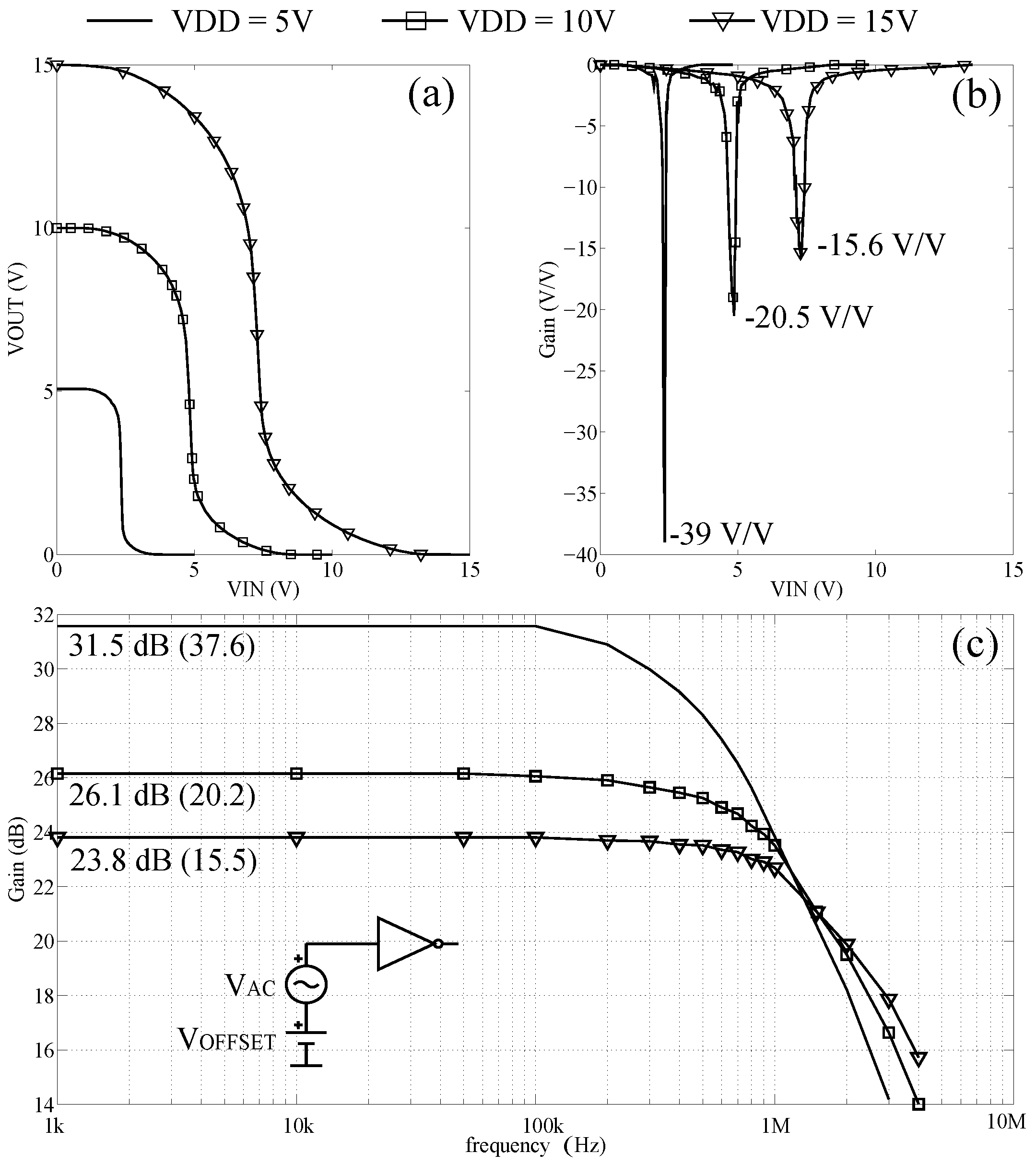
First of all, the analogue characteristics of the inverter implemented with CD4007UB and mounted in board 1 have been extracted. Voltage transfer characteristic (VTC) curve, static gain and transfer function have been measured and reported in
Figure 18 for three different values of power supply
V, 10 V, 15 V.
The static gain of the amplifier can be extracted from the VTC curve of the inverter and it represents the maximum gain achievable by this device. By increasing the value of the power supply, the static gain of the inverter decreases and the bandwidth increases almost of the same factor. The bandwidth measured are: 466 kHz, 1.06 MHz, 1.6 MHz for power supply of V, 10 V, 15 V respectively. This phenomenon is mainly due to the fact that for increasing values of the power supply, the output resistance of the inverter decreases. (, ). These measurements represent the best performance that the LL-PFGA can achieve, therefore they will be used as reference values.
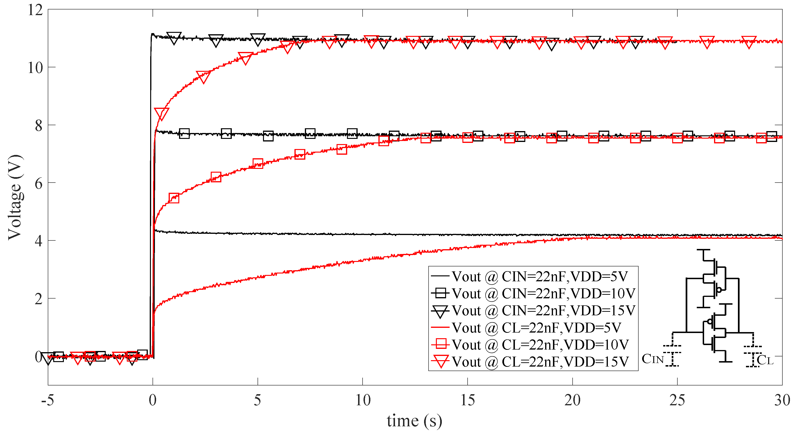
Next, the position of the bias point has been measured in a LL-PFGA, by measuring the output signal of the amplifier during the initial transient time. The measurement results are shown in
Figure 19.
The measurements in
Figure 19 have been performed for different values of power supply (5 V, 10 V, 15 V) and different values of input and output capacitance. Measurement results show that the input and the output capacitive loads do not affect the steady state value of the amplifier output voltage, but they determine the time that the input and the output signal need to approach the final value. For all of the three values of power supply, the output signal is quite far from the ideal value (
). These values are listed in
Table 5.
The input voltage of the PFGA shown in the third column of
Table 5 has been extracted by using the VTC curve of the inverter and the output voltage value. Since the bias points measured (
) are far from their ideal values (
) the PFGA will provide very low performances in terms of gain and bandwidth. The values of the bias points (
) in
Table 5 correspond approximately to the point A in
Figure 4b. Therefore, it is possible to extract the approximate values for the threshold voltage of the NMOS in the three cases, which are: 1.6 V, 2.6 V, 3.3 V for
V, 10 V, 15 V respectively. The threshold voltages measured are all greater than the value expected from
Table 4. This is due to the fact that the MOSFETs in the voltage buffer are subjected to the body effect. This phenomenon enlarges the OFF region of the voltage buffer for increasing values of power supply.
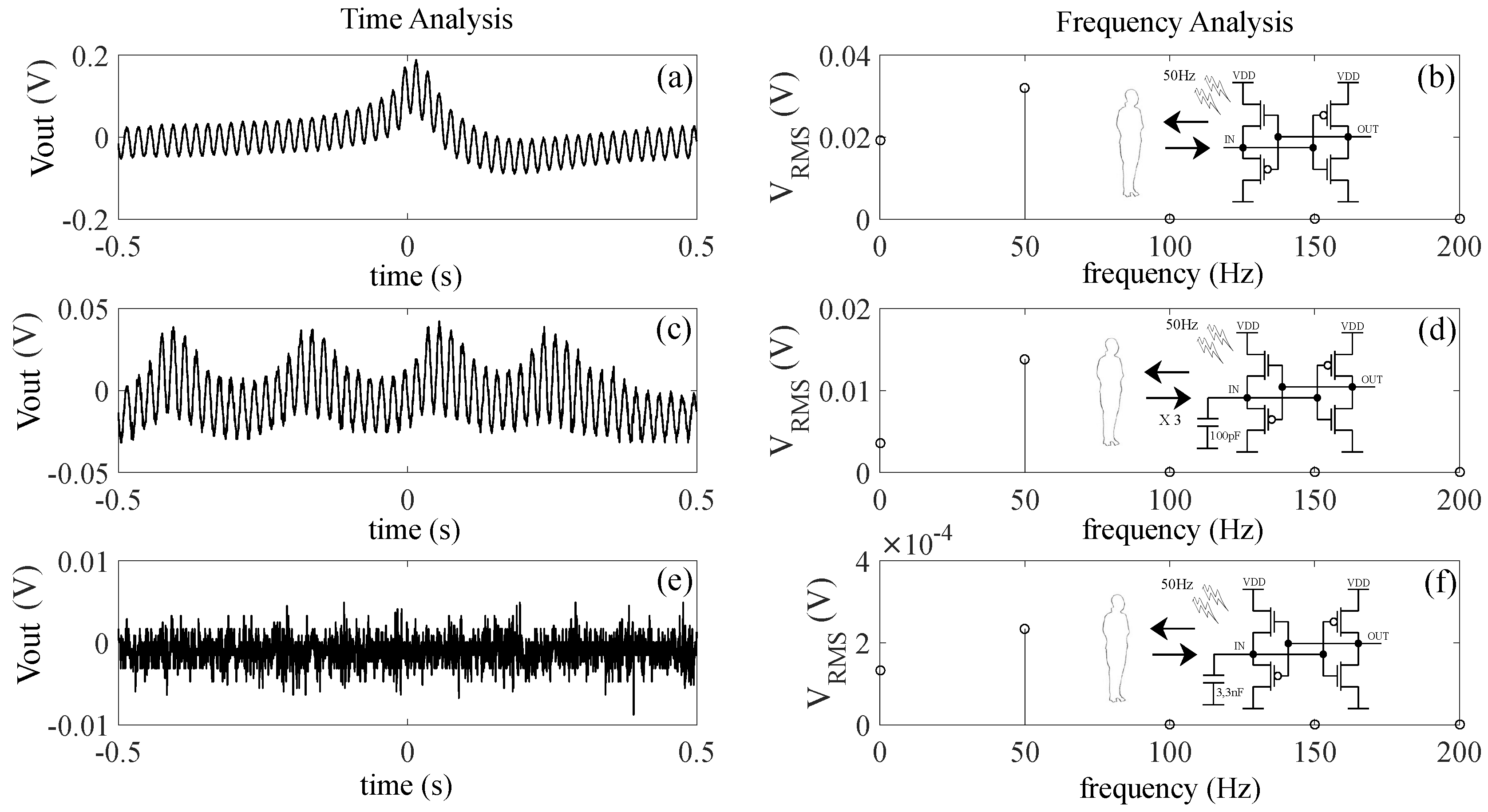
Experimental results showed that the PFGA is significantly affected by electromagnetic interferences. Two sources of noise have been observed: a 50 Hz signal and the interference due to the presence of an object close to the circuit like a human body. Measurement results are shown in
Figure 20.
Figure 20a,b shows clearly the presence of a 50 Hz component and another low frequency harmonic (a few Hz) due to the movement of a human body toward the circuit. The results in
Figure 20a,b refer to the case when the output and the input nodes are not connected to any capacitive load. The main reason of this high sensitivity to these disturbances is due to the high input resistance of the PFGA. Indeed, when the voltage buffer turns off, its output resistance approaches very high values. Therefore, when the Electromagnetic interference (EMI) induces currents at the input node of the PFGA, they are converted into voltage signals characterized by a significant amplitude. Fortunately, by creating a low impedance path to the ground for AC signals, it is possible to minimize the effects of the noises on this amplifier. The low impedance path to the ground can be realized by increasing the value of the capacitance at the input node. Measurement results for an input capacitance of 100 pF are shown in
Figure 20c,d. Finally, by using an input capacitance of
nF, the effects of the noise can be considered negligible.
Once fixed, the value of the input capacitor to increase the immunity of the circuit to the noise, it is possible to proceed with the stabilization of the bias point. This purpose is achieved by adding a voltage controlled MOSFET () to the basic structure of the PFGA. The controlled voltage of this transistor must be chosen as low as possible in order to minimize the power consumption of this MOSFET. Experimental results shows that the best value for this voltage is V, which is much lower than the threshold voltage of the NMOS, thus works in weak inversion.
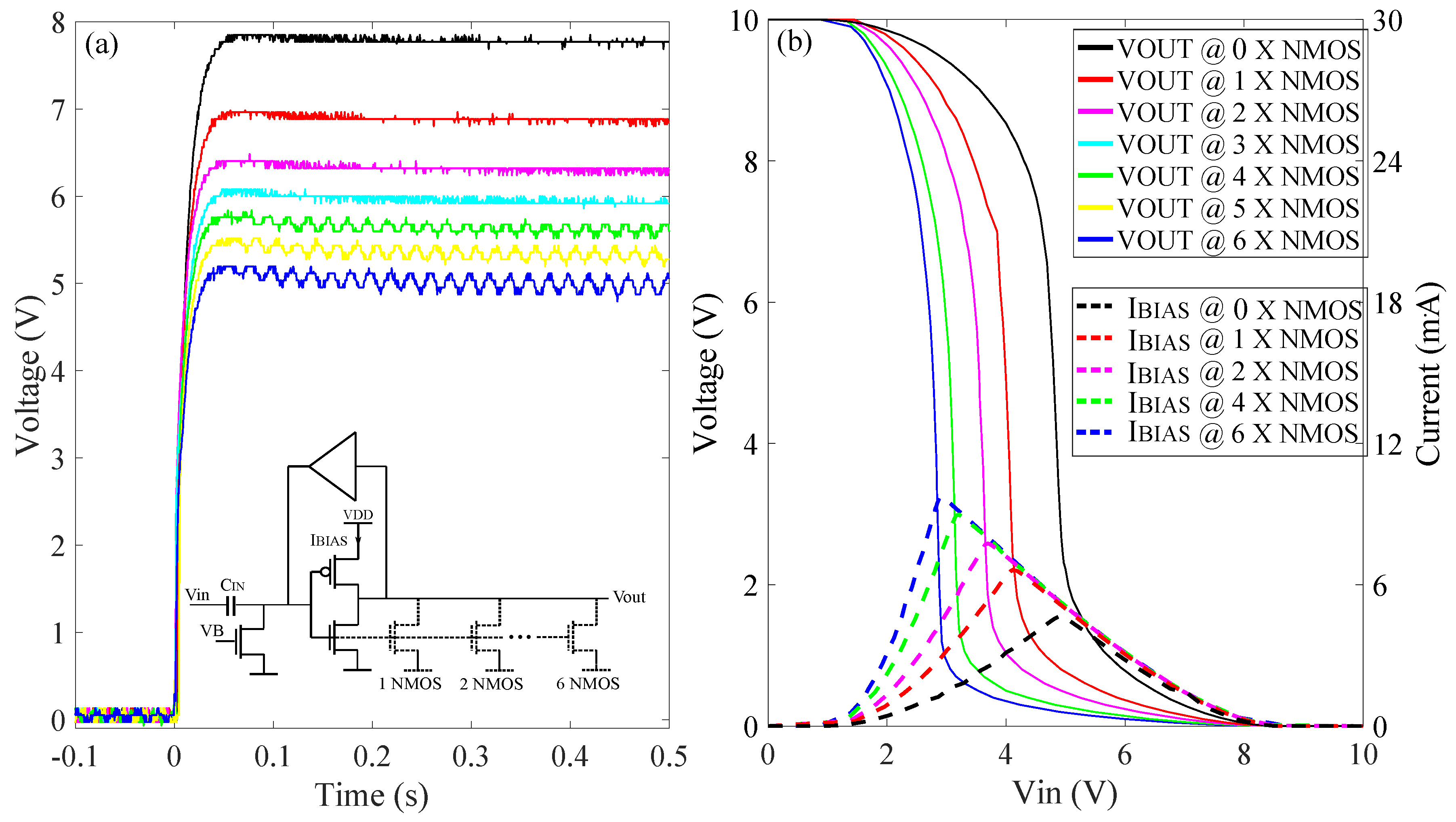
Next, multiple NMOS have been placed in parallel to
to move the equilibrium point of the PFGA toward the ideal value. This strategy has been called in this work: compensation of the PFGA offset and it moves the linear region of the inverter VTC curve to lower input values. This technique could be easily implemented during the design of a PFGA in ASIC, by choosing a high value for the width of
. However, since in this work the PFGA is realized by using commercial components, the only method to mimic the behaviour of a strong NMOS is to place them in parallel. Measurement results are shown in
Figure 21. The tests have been performed only for
V, but similar results can be obtained for other values of power supply.
Figure 21a shows that by increasing the number of parallel NMOS utilized to implement the inverter of the PFGA, the output steady state value approaches to the ideal value (
), as expected. This is due to the fact that the linear region of the inverter moves to a lower range of input voltages as shown in
Figure 21b, modifying the point of intersection with the VTC curve of the voltage buffer. The main side effect of this strategy is the increasing magnitude of the 50 Hz noise as shown in
Figure 21 for 6 parallel NMOS. This phenomenon is due to the increasing gain of the amplifier as the bias point approaches its ideal value, amplifying the input noise of the amplifier. However, this unwanted signal can be minimized by increasing the value of the input coupling capacitor
, which creates a ground path with lower impedance value for AC signals.
Figure 21b shows also that the inverter in the PFGA is characterized by an increasing biasing current as the number of parallel NMOS increases. This is due to the fact that the equivalent resistance of the N-branch of the inverter decreases. A more compact circuit can be implemented by using 2N7000 (Fairchild, Sunnyvale, CA, USA) as NMOS of the inverter in the PFGA rather than using multiple NMOS in parallel. 2N7000 is a NMOS that can handle a current around hundred times greater than the current provided by the CD4007UB (NMOS) under the same conditions. Therefore, it is expected that 2N7000 is characterized by greater channel width. The prototype realized by using this component is shown in
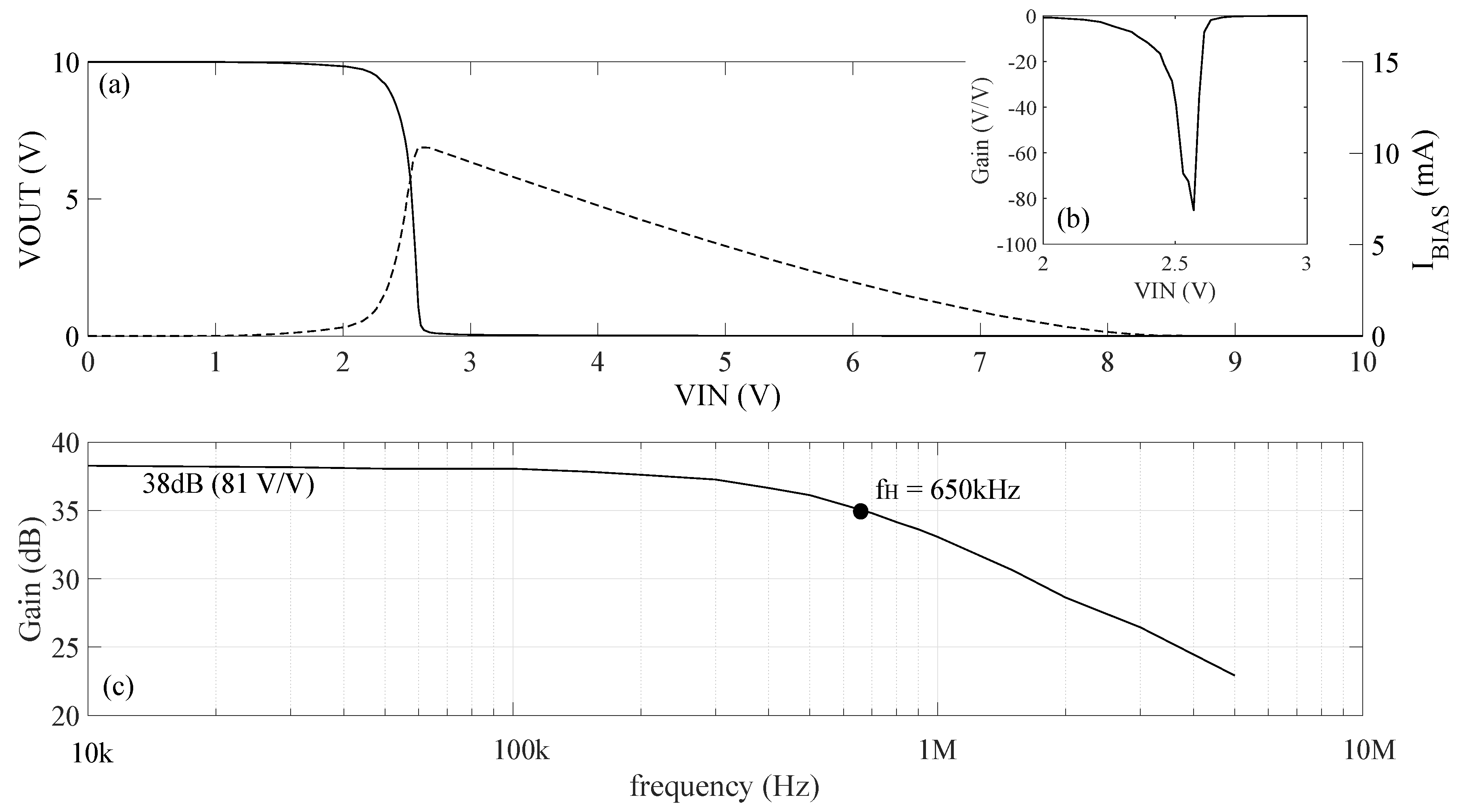
Figure 22.
The value of the input capacitance has been chosen as 100 nF, to avoid any effect of EMI on the circuit. The NMOS (
) is controlled by a constant voltage of
V. The performances of this prototype have been extracted and represented in
Figure 23.
Figure 23a shows that both the distribution of the VTC curve and the bias current of the inverter in the PFGA are asymmetric along the input voltage range.
Figure 23b shows a static gain 4 times greater than the one characterizing an inverter purely implemented with CD4007UB as shown in
Figure 18b.
Figure 23c shows the frequency response of the PFGA, which presents a high cut-off frequency at 650 kHz, almost half of the value obtained for a CD4007UB inverter shown in
Figure 18c. The frequency response of the PFGA has been measured by loading the amplifier with an oscilloscope (Agilent Technologies (Santa Clara, CA, USA) InfiniiVision DSO-X 3032A
pF,
M). The gain of the LL-PFGA is greater than the case represented in
Figure 18, because the NMOS of the LL-PFGA has a greater transconductance (
) due to the lower overdrive voltage (
). Indeed, by moving the linear region of the inverter to lower values then
decreases. This phenomenon can be also represented mathematically as shown in Equations (
3)–(
5).
Assuming similar values of
then:
Since :
then
Equation (
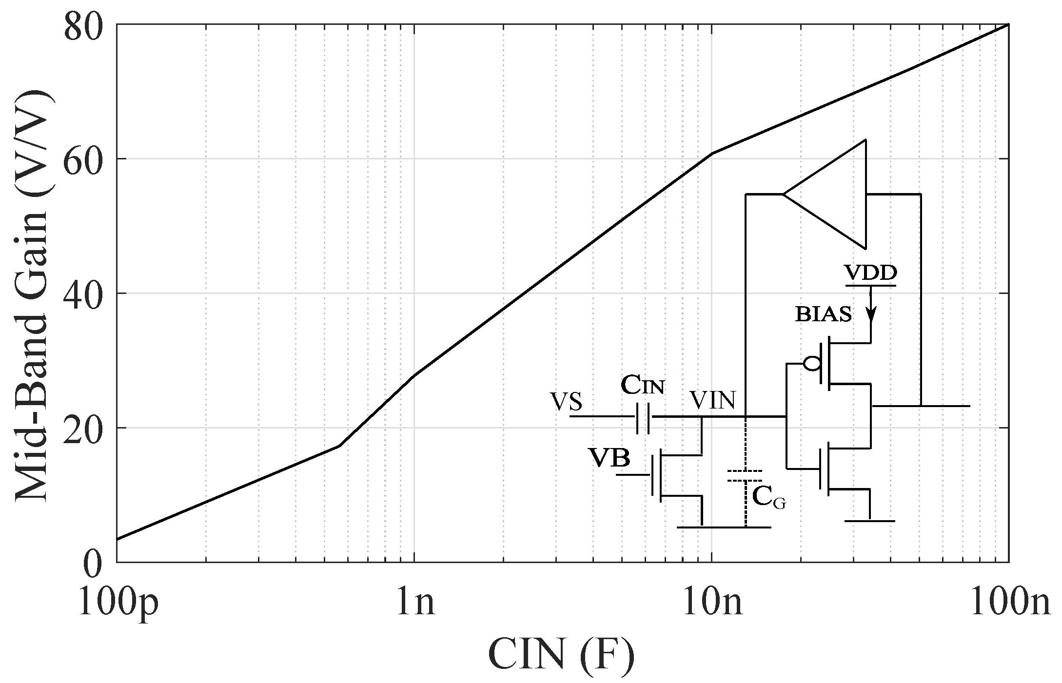
5) shows analytically that a low value of the NMOS overdrive voltage increases the gain of the inverter, so of the PFGA. Another interesting phenomenon is the dependency of the mid band gain from the value of
, as shown in
Figure 24This phenomenon is due to the input voltage divider composed of
and
, which reduces the contribution of
to the input of voltage (
) of the PFGA, when
decreases. Equation (
6) shows the voltage divider formulas.
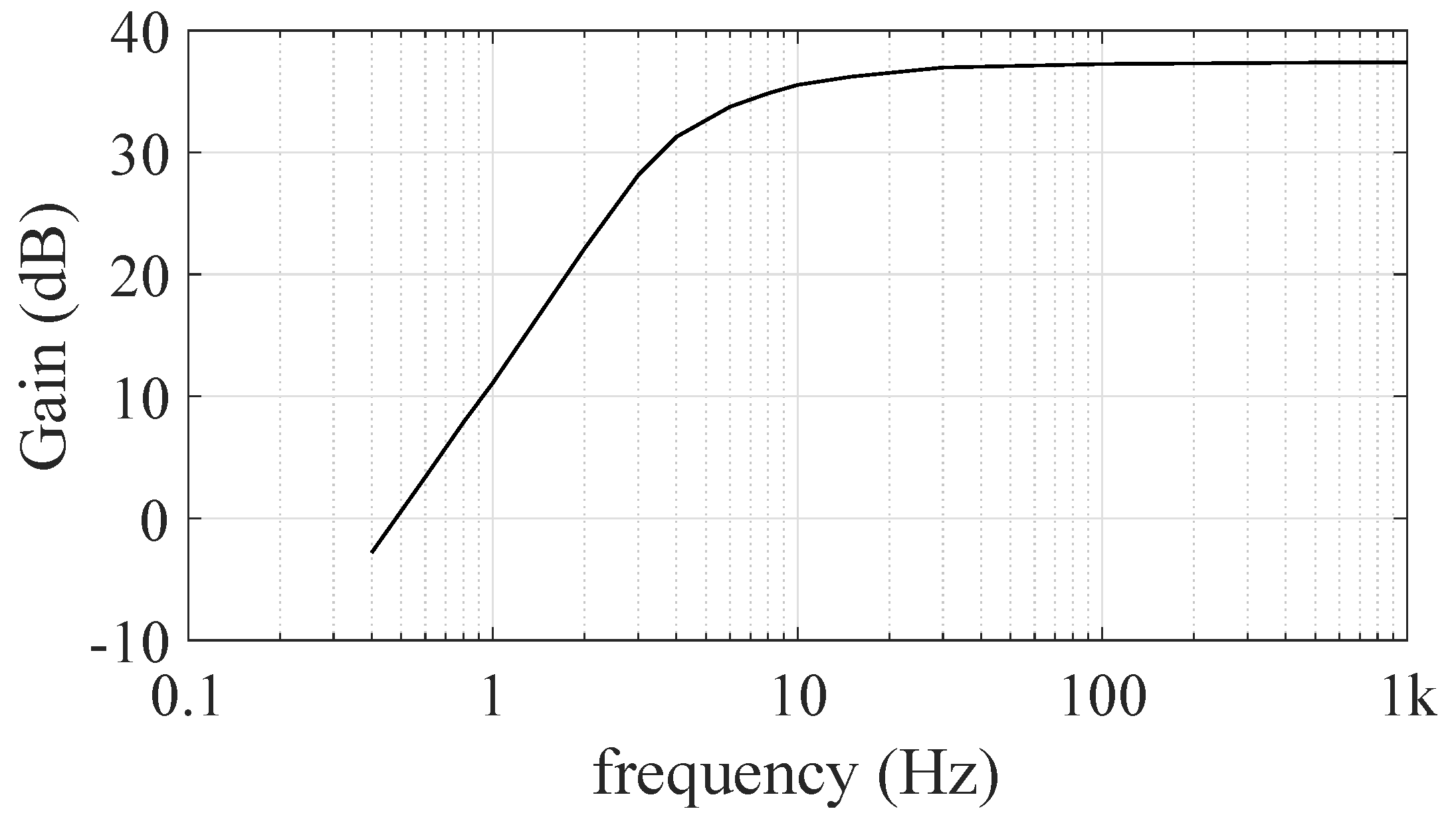
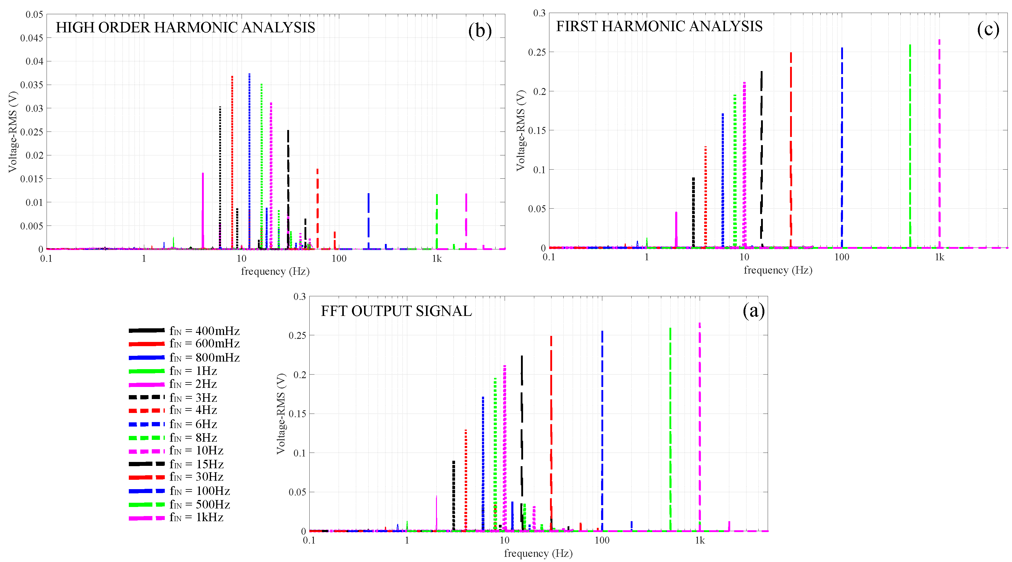
Finally, the behaviour of the PFGA at low frequency has been analyzed. Measurement results are shown in
Figure 25 and
Figure 26.
The measurement results in
Figure 25 refer to a sweep in the frequency of the input signal in a range of [0.1 Hz,1 kHz]. The frequency response of the PFGA represented in
Figure 25 shows the non linear behaviour of the amplifier around the low cut-off frequency.
Figure 25a shows the total output signal spectrum,
Figure 25b shows only the harmonics of the output signal generated by the non linearities of the amplifier and
Figure 25c shows only the fundamental harmonics of the output signal for each iteration of the sweep.
Figure 26 shows the frequency response of the amplifier calculated by considering the ratio between the fundamental harmonic of the output and the amplitude of the input source voltage (
). The amplifier shows a low cut-off frequency of 5 Hz.


