Design and optimization of collection efficiency and conversion gain of buried p-well SOI pixel X-ray detector

1
Chinese Academy of Sciences, Shanghai Advanced Research Institute, Shanghai 200000, China
2
Department of Electrical and Computer Engineering, George Mason University, Fairfax, VA 22030, USA
*
Authors to whom correspondence should be addressed.
Electronics 2017, 6(2), 26; https://doi.org/10.3390/electronics6020026
Submission received: 22 December 2016
/
Revised: 6 March 2017
/
Accepted: 20 March 2017
/
Published: 23 March 2017
Abstract
:Buried P-Well (BPW) technology was used in silicon-on-insulator pixels (SOIPIX) to suppress the back-gate effect, the major challenge in SOIPIX. In this work, we have designed and optimized two novel pixel structures, which are based on different BPW design layouts, to study the carrier collection efficiency and conversion gain of the pixel unit used in SOIPIX X-ray detectors. The first structure has an extended BPW region connected with a P+ node. In the second structure, a separated BPW ring region is formed surrounding the P+ node. Two X-ray sources with different photon energies have been applied in the simulation of excess carrier generation. The results indicated that the first structure had higher collection efficiency while the second structure had a slightly better conversion gain. As a result, the total photoelectric voltage of the first structure is about two times that of the second structure, where low doping concentration (<1 × 1016 cm‒3) in the BPW region is preferred. Such a study of design and optimization of BPW technology is very important for applications in SOIPIX detectors.
1. Introduction
In the field of medical diagnostics, digital X-ray imaging systems have been under investigation and development for a long time [1]. According to the different conversion principles, there are two kinds of X-ray imaging systems, direct and indirect systems [2]. The indirect imaging system first converts X-ray information to visible light by using scintillators and then converts the visible light into electrical signals through photodiodes [3]. The direct imaging system directly converts the X-ray information into electrical signals by using an X-ray conversion film (i.e., X-ray photoconductor). Since the direct system does not need scintillators, energy absorption efficiency can be improved and the inherent deterioration of spatial resolution can be avoided [3,4].
The SOI X-ray detectors have recently been integrated in the direct imaging system [5]. Some progress in this area has been achieved by Miyoshi et al. [6,7,8], who studied X-ray astronomy with SOI CMOS technology. Niemiec et al. have also researched monolithic X-ray detectors with thick film SOI technology [9]. These detectors are composed of a thick, high-resistivity substrate (the X-ray absorption layer) and a relatively thin, low-resistivity Si layer (on which to build readout circuits) sandwiching a buried oxide (BOX) layer in a single wafer. It is different with the conventional hybrid X-ray detectors in which the detector chips and readout circuit chips are fabricated on different wafers [10].
Compared with the conventional bulk CMOS circuits, the readout circuits fabricated on the SOI wafer have less parasitic capacitance due to the thin top Si layer, enabling higher speed and lower power consumption [11]. The SOI-based circuits are quite immune to latch-up phenomena [12]. In addition, since the active SOI transistor is very thin, most radiation-induced electron-hole pairs are blocked by the BOX layer, and the SOI device is less sensitive to single event upset (SEU) and single event transient (SET) [13].
As mentioned above, SOI detectors are very promising for X-ray imaging. However, it should be noticed that SOIPIX is difficult to be implemented in circuits [14]. One of the major challenges is the back-gate effect: the silicon substrate under the BOX layer acts as a back gate for the transistors built on SOI. Therefore, the potential of silicon substrate affects the threshold voltage and leakage current of the transistors [15]. Buried P-Well (BPW) technology has been proposed by KEK [16,17] to suppress the back-gate effect. In addition, BPW has an impact on the pixel characteristics because it affects the carrier collection process. In this work, in order to optimize the collection efficiency and the conversion gain, we have designed and optimized SOIPIX X-ray detectors with different BPW structures. By varying the size and position of the buried P-Well, we have studied the dependence of the collection efficiency and the conversion gain on device geometry. We have also studied the impact of BPW doping concentration on the pixel characteristics.
2. Pixel Structure
This study is based on a fully-depleted (FD) SOI 0.2 μm process [18,19]. In this design and simulation, the SOI wafer consists (after thinning) of a 260 μm thick, N-type, 700 Ω/cm Si substrate, 200 nm thick BOX and a 40 nm thick SOI on which the readout circuits are fabricated. In this work, a diode structure has been used in the design and simulation of X-ray pixel sensors in the Si substrate.
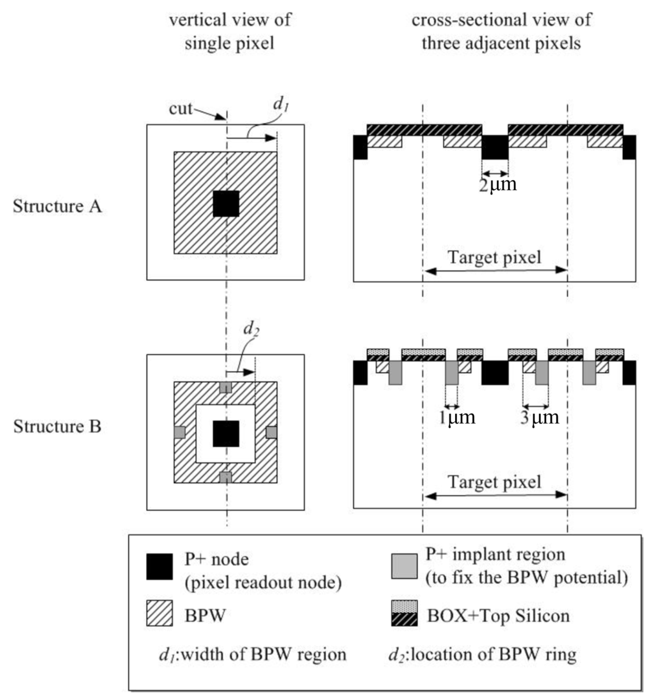
The device configurations A and B are shown in Figure 1. First, a “window” is opened in the BOX and SOI. Through the window, a P-type doping region is designed to form a P+ node (doping concentration ≈ 1 × 1020 cm‒3, depth = 1 μm). The P+ node is used to connect to the readout circuits. Another important doping region is BPW, which is used to suppress the back-gate effect. The doping level in the BPW region (depth = 0.3 μm) is about three orders lower than that in the P+ node. d1 is the half width of BPW in structure A. d2 is the separation distance between BPW ring and pixel center. The detailed explanation of these structures is shown in Table 1. To reverse-bias the photodiode, 400 V is applied at the bottom contact of the N-type Si substrate [20]. Under such a high reverse-bias voltage, full depletion can be achieved in the Si substrate. In addition, two neighboring pixels separated by 20 μm were added to eliminate the boundary effect. The recombination process in the substrate is modeled with the Shockley-Read-Hall model and the lifetime is set as 1 μs. The top silicon is grounded. The BPW ring in structure B is reset as 0 V and will remain floating during the carrier collection process.
3. Incident X-ray Penetration Model
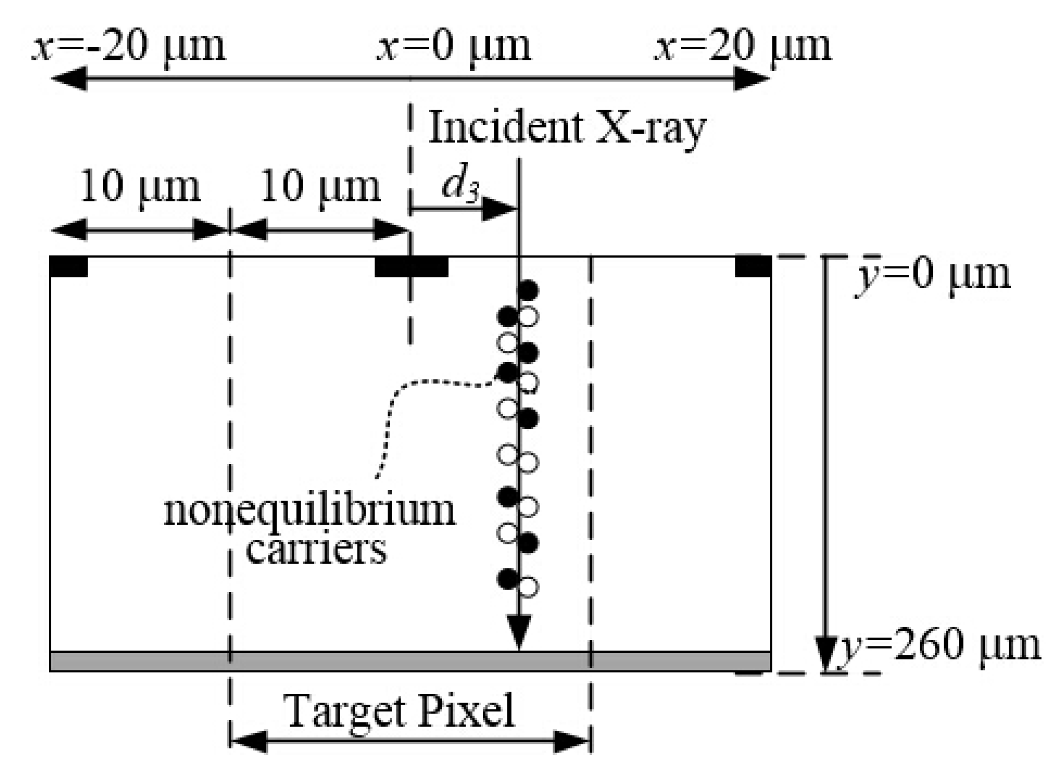
After the design of devices, the X-ray detector is simulated and analyzed. Penetration location (d3) refers to the distance between the X-ray hitting point and the target pixel center. As shown in Figure 2, d3 has been scanned (from 0 to 7 μm) during the pixel simulation.
In this work, the HeavyIon model [21] has been applied to simulate the generation of non-equilibrium carriers. This model is used to define the linear energy transfer (LET). Therefore, it is applicable in modelling the photoelectric effect of incident X-rays. In this work, LET values are computed based on the datasheet of X-ray sources used in the research of Nishimura et al. [22], where two monochromatic X-ray (33.3 keV and 9.5 keV) stations were used. The detailed parameters used in this work are shown in Figure 3.
4. Simulation Results
4.1. Electric Potential Distribution
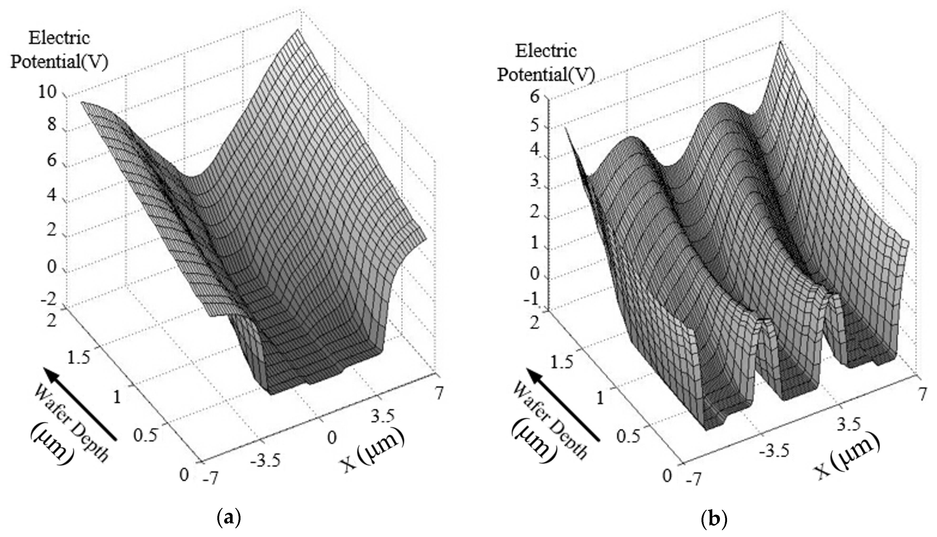
In order to study the carrier collection process in different pixel structures, the electric potential distribution has been simulated. As the photodiode is reverse-biased with a high voltage, the depletion region expands to nearly the whole substrate [23]. Therefore, different pixel structures have the same potential distribution in the region far away from the P+ anode or BPW, namely the region at y > 10 μm. The potential distribution in these remote regions can be considered by using a simple PN junction model.
However, the electric potential profile of the region close to the pixel P+ node exhibits large differences. As shown in Figure 4, in Structure A, the potential in the extended BPW region is pinned to ground through the P+ node. The potential well induced by the BPW region is connected to the one induced by the P+ node. Therefore, the total space of potential wells which can collect carriers is expanded [24]. In Structure B, the BPW ring is separated from the P+ node, which exhibits three separated potential wells in the two-dimensional (2D) cross-section view.
4.2. Carrier Collection Efficiency
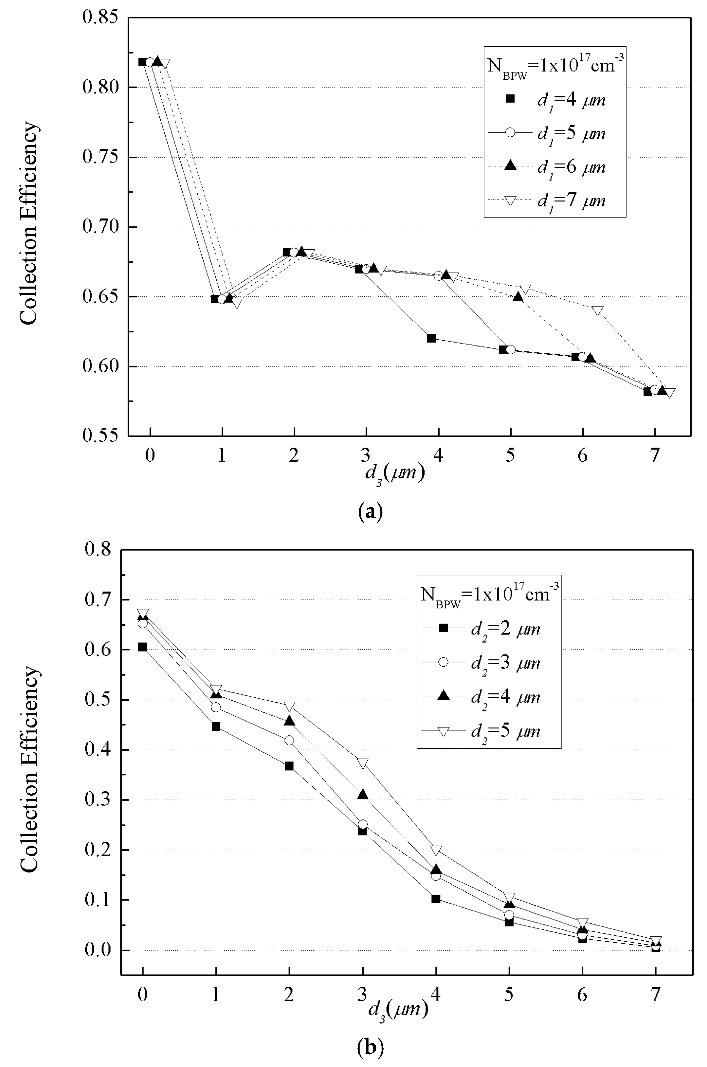
During the carrier collection process, the non-equilibrium carriers cannot be completely collected by the target pixel due to carrier lateral diffusion, carrier recombination, and trapping effects [25]. We simulated the collection efficiency of different pixel structures and compared the results by considering all these effects. Here, the carrier efficiency was defined as a ratio of the number of carriers collected by the target pixel over the number of carriers generated in the whole absorption layer [26].
The simulation results shown in Figure 5 illustrate the influence of BPW size (in structure A) and BPW ring location (in structure B) on the collection efficiency with a 33.3 keV X-ray source applied. In Structure A, higher collection efficiency can be obtained with larger BPW. This is because, with the larger expanded BPW region, more holes can be collected by the expanded potential well. It is also noticed that the collection efficiency slightly decreases when d3 (i.e., the distance between the X-ray hitting point and the target pixel center) increases. The decrease of the collection efficiency is mainly due to the carrier recombination in the bulk and the region beneath the surface. It is found that when d3 = 7 μm, half of the excess carriers are recombined in the bulk or in the surface. Only less than 9% of the carriers are collected by neighboring pixels. It should be noted that the carrier collection can be significantly affected by the substrate and interface/surface quality. This is not the focus of this work and will be further investigated in future research.
In structure B, the collection efficiency is much more sensitive to the X-ray penetration location. Most of the lost carriers are collected by the BPW ring. When d3 is 4 μm, nearly half of excess carriers are collected by the BPW ring and the number of carriers diffusing to the next pixel decreases to less than 5%.
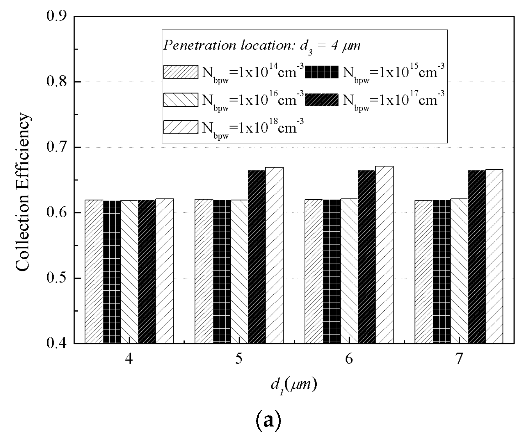
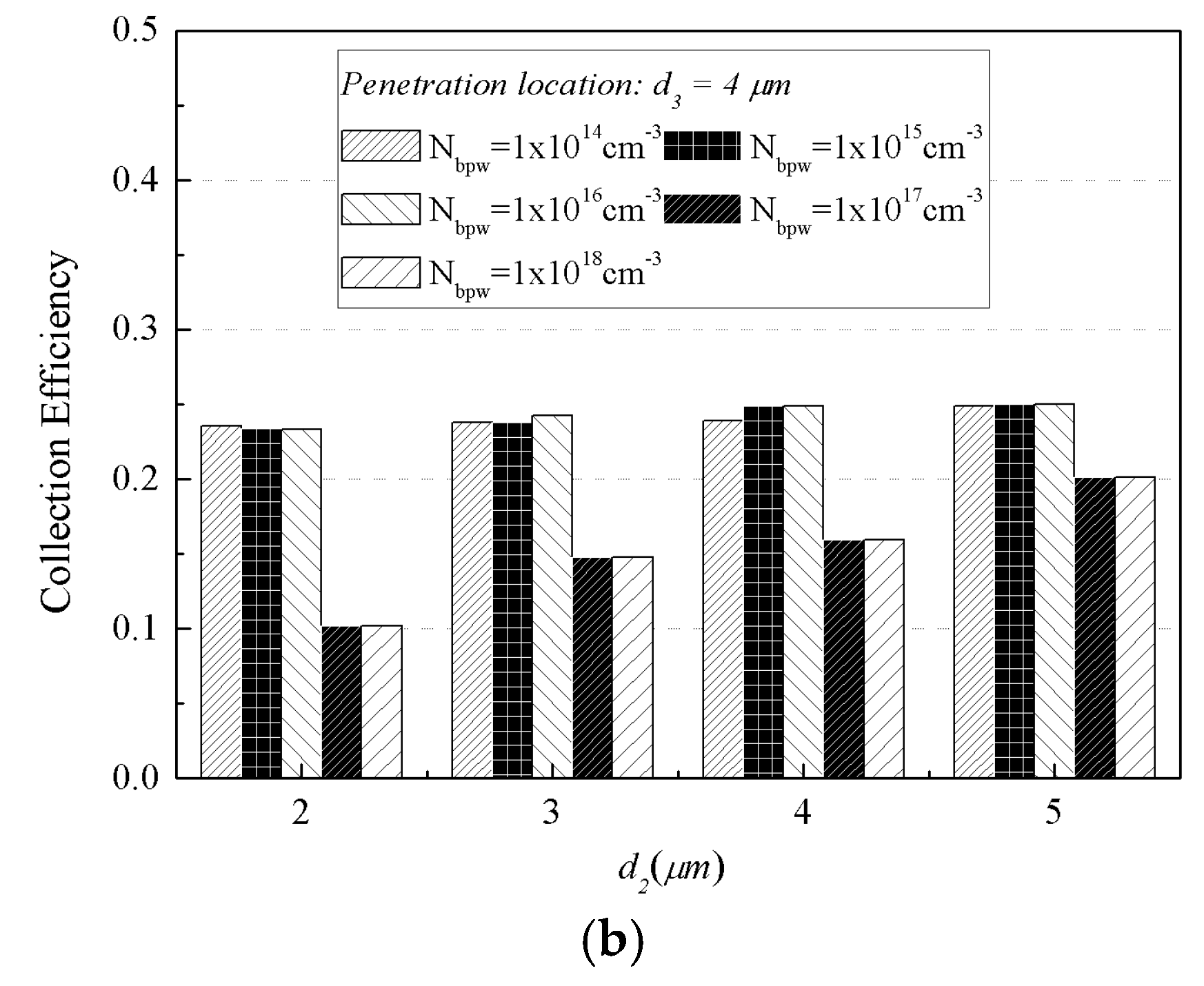
We also studied the influence of BPW doping concentration on the collection process with 33.3 keV X-ray source applied. The penetration location has been set as d3 = 4 μm to better illustrate the doping concentration effect. This is because the BPW effect is relatively less obvious with shorter d3. It is expected that the collection efficiency can be improved with the larger BPW in Structure A according to the results in Figure 5. Indeed, as shown in Figure 6 the improvement is achieved only when BPW doping concentration is large enough (>1 × 1017 cm‒3). While in Structure B, low concentration of BPW is preferred in order to obtain higher collection efficiency. This is because the BPW ring in structure B can collect more carriers with higher doping concentration, while those carriers are not collected by the target pixel node.
Through the integration of the collection efficiency with the X-ray penetration location (shown in Figure 5), it is found that the ratio of the collection efficiency in Structure A and in Structure B is 2.15–2.22. A high ratio can be achieved with a high BPW doping concentration and large BPW in Structure A.
As two X-ray sources were studied in our research, the effect of different photon energy has been compared. As shown in Figure 7, the pixel exhibits higher collection efficiency with 9.9 keV X-ray source in both structure A and structure B. This effect is related to the shallow energy deposition location of the X-ray with small photon energy. For a 9.9 keV X-ray source, most carriers are generated close to the collection node and their lateral diffusion and recombination would be suppressed.
4.3. Conversion Gain
As discussed above, BPW technology, indeed, creates an additional potential well which is beneficial to the improvement of the carrier collection efficiency. However, it also increases the pixel capacitance, which may decrease the conversion gain [27]. In this work, we have re-designed the pixel with different BPW doping concentration to achieve the optimal conversion gain.
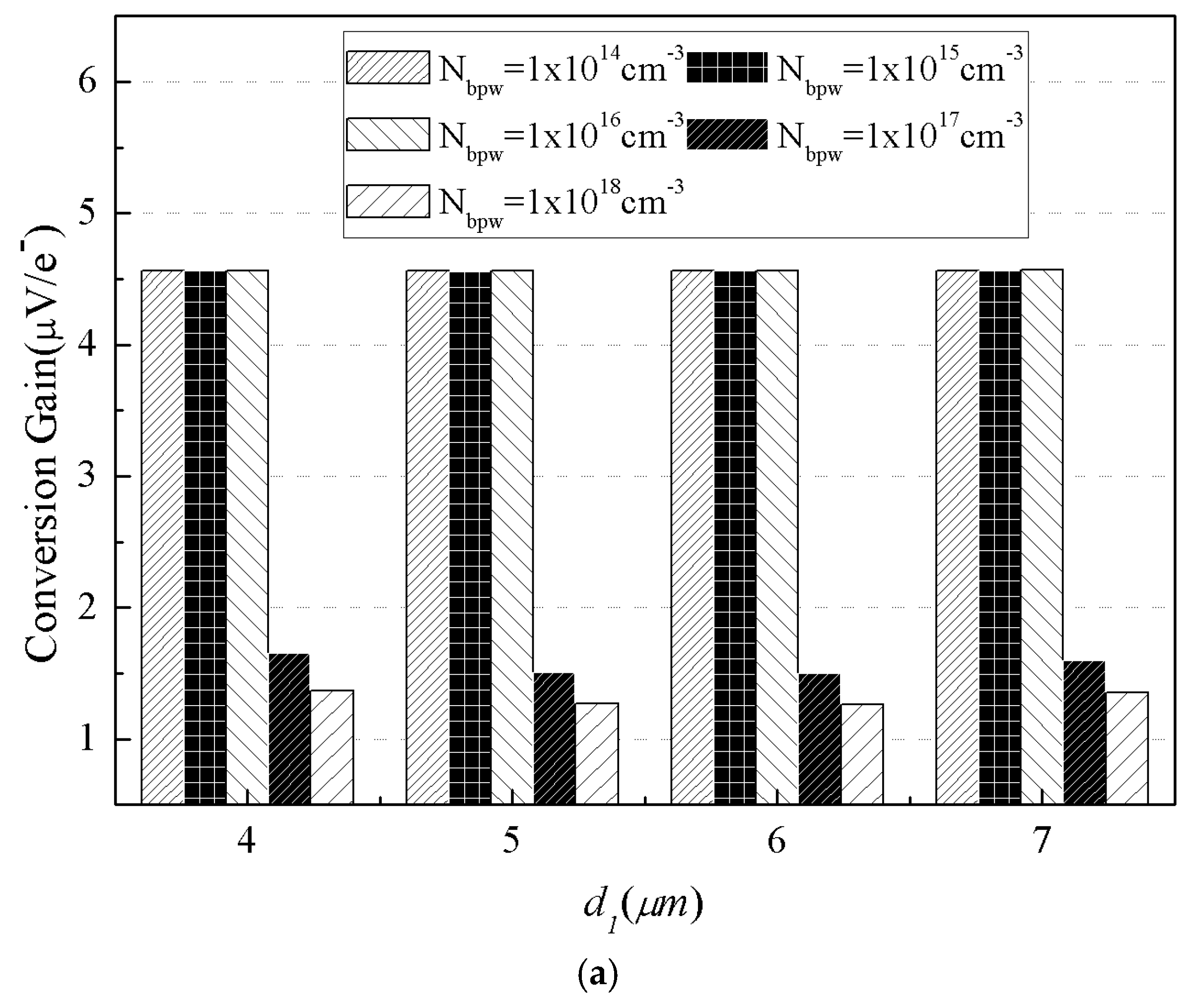
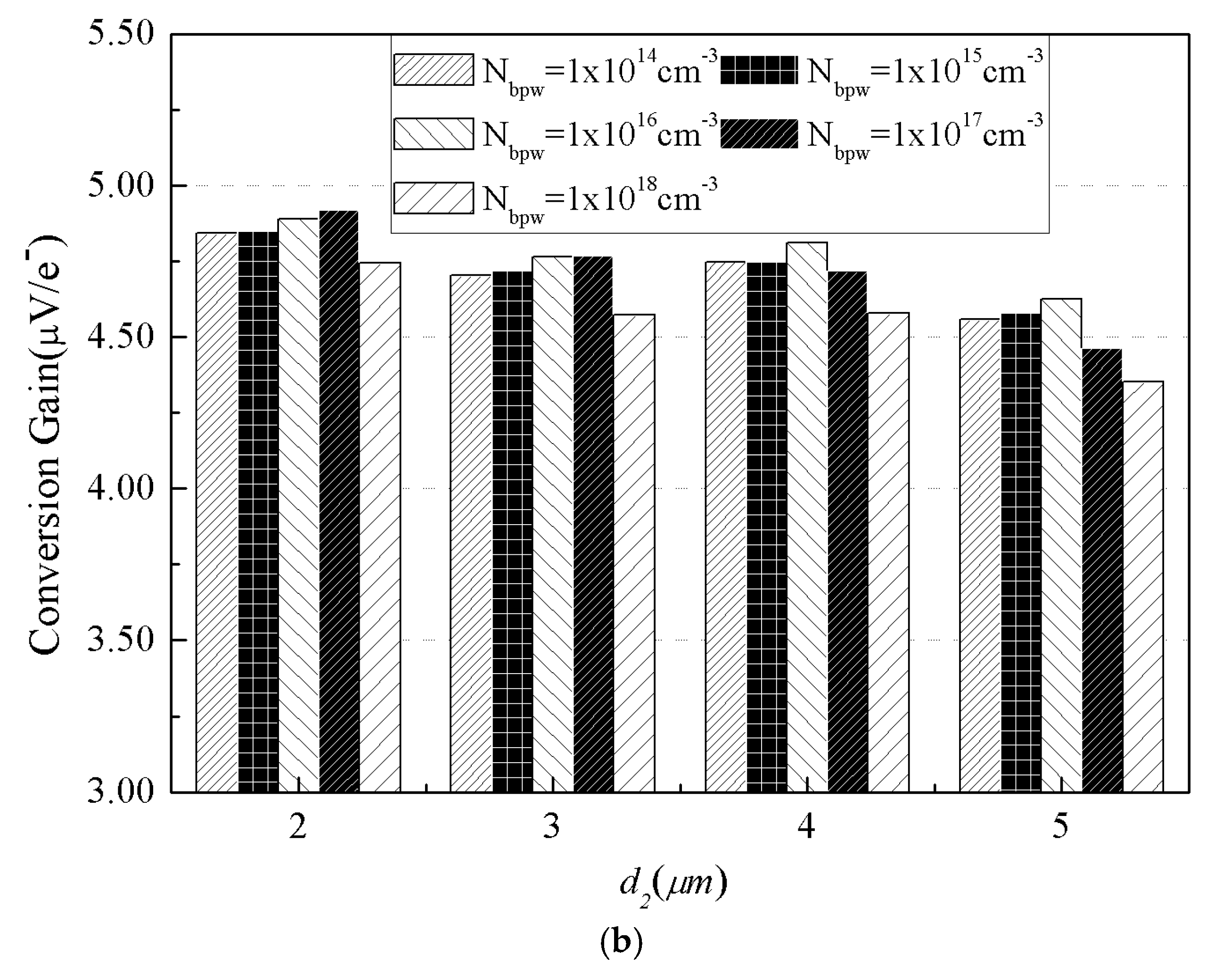
Figure 8 shows the conversion gain with a 33.3 keV X-ray source. It is found that the influence of BPW doping concentration on the conversion gain is more significant in Structure A. The conversion gain decreases to 1.5 μV/e− from 5 μV/e− when the BPW doping concentration increases to 1 × 1017 cm−3. In Structure B, the conversion gain is not significantly affected by the doping concentration and the location of the BPW ring. The gap between the P+ node and the BPW ring is so large that the carriers collected in the BPW ring will not affect the voltage of the P+ node. The ratio of the conversion gain in Structure A and Structure B is about 0.93–0.31. A high ratio can be obtained with low BPW doping concentration in structure A.
The same conversion gain is also obtained with a 9.5 keV X-ray source. This makes sense since the conversion gain is mostly decided by the pixel structure, but not affected by the incident X-ray photon energy.
5. Conclusions
In this work, we have designed and optimized two novel SOI pixel structures based on BPW technology. The photoelectric effect of two X-ray sources with different photon energy has been modeled in the simulation. We found that larger extended BPW could offer better collection efficiency. This improvement of collection efficiency prefers a high doping concentration of the BPW region. For the pixel with a separated BPW ring, the large separation between the BPW ring and the P+ node is preferred. Additionally, the low doping concentration of BPW ring offers better carrier collection efficiency in this structure. For the conversion gain optimization, a low doping concentration of the BPW is preferred in the pixel with the extended BPW. However, in the pixel with the separated BPW ring, the conversion gain only varies slightly with the different location and doping concentration of the BPW ring. Taking both carrier collection efficiency and conversion gain into account, the photoelectric voltage of the pixel with the extended BPW is about two times that of the pixel with the separated BPW ring, where the low doping concentration of BPW is preferred. This study of design and optimization of BPW technology is very important for applications in SOIPIX detectors
Acknowledgments
This work is financially supported by the Chinese National Major Science and Technology Projects under grant no. 2011ZX02505, and Shanghai Municipal Science and Technology Commission under grant no. 13511501000 and no. 14511102302. C. Shi and Q. Li acknowledge the support of the Virginia Microelectronics Consortium research fund.
Author Contributions
Hui Wang and Chen Shi designed the research and process. Chen Shi performed the simulation. Hui Wang, Li Tian, Chen Shi, Songlin Song, and Qiliang Li analyzed the data. Chen Shi wrote the manuscript. Hui Wang and Qiliang Li revised the manuscript.
Conflicts of Interest
The authors declare no conflict of interest. The founding sponsors had no role in the design of the study; in the collection, analyses, or interpretation of data; in the writing of the manuscript, and in the decision to publish the results.
References
- Seibert, J.A. One hundred years of medical diagnostic imaging technology. Health Phys. 1995, 69, 695–720. [Google Scholar] [CrossRef] [PubMed]
- Prekas, G.; Sabet, H.; Bhandari, H.H.; Derderian, G.; Robertson, F.; Kudrolli, H.; Stapels, C.; Christian, J.; Kleinfelder, S.; Cool, S.; et al. Direct and indirect detectors for X-ray photon counting systems. In Proceedings of the 2011 IEEE Nuclear Science Symposium and Medical Imaging Conference (NSS/MIC), Valencia, Spain, 23–29 October 2011; pp. 1487–1493. [Google Scholar]
- Seibert, J.A. X-ray Imaging Physics for Nuclear Medicine Technologists. Part 1: Basic Principles of X-ray Production. J. Nucl. Med. Technol. 2004, 32, 139–147. [Google Scholar] [PubMed]
- Overdick, M.; Bäumer, C.; Engel, K.J.; Fink, J.; Herrmann, C.; Kruger, H.; Simon, M.; Steadman, R.; Zeitler, G. Status of Direct Conversion Detectors for Medical Imaging With X-rays. IEEE Trans. Nucl. Sci. 2009, 56, 1800–1809. [Google Scholar] [CrossRef]
- Ryu, S.G.; Tsuru, T.G.; Nakashima, S.; Takeda, A.; Arai, Y.; Miyoshi, T.; Ichimiya, R.; Hironori, I.; Matsumoto, H.; Imamura, T.; et al. First Performance Evaluation of an X-ray SOI Pixel Sensor for Imaging Spectroscopy and Intra-Pixel Trigger. IEEE Trans. Nucl. Sci. 2011, 58, 2528–2536. [Google Scholar] [CrossRef]
- Miyoshi, T.; Arai, Y.; Hirose, M.; Ichimiya, R.; Ikemoto, Y.; Kohriki, T.; Tsuboyama, T.; Unno, Y. Performance study of SOI monolithic pixel detectors for X-ray application. Nucl. Instrum. Methods 2011, 636, S237–S241. [Google Scholar] [CrossRef]
- Hideaki, M.; Takeshi, G.T.; Takaaki, T.; Shinya, N.; Syukyo, G.R.; Ayaki, T.; Yasuo, A.; Toshinobu, M. Investigation of charge-collection efficiency of Kyoto’s X-ray astronomical SOI pixel sensors, XRPIX. Nucl. Instrum. Methods 2014, 765, 183–186. [Google Scholar]
- Tsuru, T.G.; Matsumura, H.; Takeda, A.; Tanaka, T.; Nakashima, S.; Arai, Y.; Mori, K.; Takenaka, R.; Nishioka, Y. Development and Performance of Kyoto’s X-ray Astronomical SOI pixel (SOIPIX) sensor. Proc. SPIE 2014, 9144. [Google Scholar] [CrossRef]
- Niemiec, H.; Jastrzab, M.; Kucewicz, W.; Kucharski, K.; Marczewski, J.; Sapor, M.; Tomaszewski, D. Full-size monolithic active pixel sensors in SOI technology-Design considerations, simulations and measurements results. Nucl. Instrum. Methods 2006, 568, 153–158. [Google Scholar] [CrossRef]
- Gregory, P.; Vyshnavi, S.; David, P.; Richard, F.; Steve, K.; Beverly, L.; Antonio, M.S.; Joel, V.; Marshall, B. Characterization of Three-Dimensional-Integrated Active Pixel Sensor for X-ray Detection. IEEE Trans. Electron. Devices 2009, 56, 2602–2611. [Google Scholar]
- Hu, Y.; Deptuch, G.; Turchetta, R.; Guo, C. A low-noise, low-power CMOS SOI readout front-end for silicon detector leakage current compensation with capability. IEEE Trans. Circuits. Syst. I Fundam. Theory Appl. 2001, 48, 1022–1030. [Google Scholar] [CrossRef]
- Tierno, J.A.; Rylyakov, A.V.; Friedman, D.J. A Wide Power Supply Range, Wide Tuning Range, All Static CMOS All Digital PLL in 65 nm SOI. IEEE J. Solid-State Circuits 2008, 43, 42–51. [Google Scholar] [CrossRef]
- Iwata, H.; Ohzone, T. Numerical analysis of alpha-particle-induced soft errors in SOI MOS devices. IEEE Trans. Electron. Devices 1992, 39, 1184–1190. [Google Scholar] [CrossRef]
- Marczewski, J.; Caccia, M.; Domanski, K.; Grabiec, P.; Grodner, M.; Jaroszewicz, B.; Klatka, T.; Kociubinski, A.; Koziel, M.; Kucewicz, W.; et al. Monolithic silicon pixel detectors in SOI technology. Nucl. Instrum. Methods 2005, 549, 112–116. [Google Scholar] [CrossRef]
- Schwantes, S.; Furthaler, J.; Schauwecker, B.; Dietz, F.; Graf, M.; Dudek, V. Analysis of the Back-Gate Effect on the on-State Breakdown Voltage of Smartpower SOI Devices. IEEE. Trans. Device Mater. Reliab. 2006, 6, 377–385. [Google Scholar] [CrossRef]
- Miyoshi, T. Recent progress in development of SOI pixel detectors. In Proceedings of the 2010 IEEE Nuclear Science Symposium Conference Record (NSS/MIC), 30 October–6 November 2010; pp. 1885–1888. [Google Scholar]
- Arai, Y.; Miyoshi, T.; Unno, Y.; Tsuboyama, T.; Terada, S.; Ikegami, Y.; Ichimiya, R.; Kohriki, T.; Tauchi, K.; Ikemoto, Y.; et al. Development of SOI pixel process technology. Nucl. Instrum. Methods 2011, 636, S31–S36. [Google Scholar] [CrossRef]
- Arai, Y.; Miyoshi, T.; Unno, Y.; Tsuboyama, T.; Terada, S.; Ikegami, Y.; Kohriki, T.; Tauch, K.; Ikemoto, Y.; Ichimiya, R.; et al. Developments of SOI monolithic pixel detectors. Nucl. Instrum. Methods 2010, 623, 186–188. [Google Scholar] [CrossRef]
- Toshinobu, M.; Yasuo, A.; Tadashi, C.; Yowichi, F.; Kazuhiko, H.; Shunsuke, H.; Yasushi, I.; Yoichi, I.; Yukiko, K.; Takash, K.; et al. Monolithic pixel detectors with 0.2 um FD-SOI pixel process technology. Nucl. Instrum. Methods 2013, 732, 530–534. [Google Scholar]
- Prigozhin, G.; Gendreau, K.; Bautz, M.W.; Burke, B.; Ricker, G. The depletion depth of high resistivity X-ray CCDs. IEEE Trans. Nucl. Sci. 1998, 45, 903–909. [Google Scholar] [CrossRef]
- Synopsys Inc. Guide, Sentaurus Device User, version E; Synopsys Inc.: Mountain View, CA, USA, 2010; pp. 489–498. [Google Scholar]
- Ryutaro, N.; Yasuo, A.; Toshinobu, M.; Keiichi, H.; Shunji, K.; Ryo, H. Development of an X-ray imaging system with SOI pixel detectors. Nucl. Instrum. Methods 2016, 831, 49–54. [Google Scholar] [CrossRef]
- Knoll, G.F. Radiation Detection and Measurement; John Wiley & Sons: Hoboken, NJ, USA, 2010; p. 390. [Google Scholar]
- Poudel, A.; McDermott, R.; Vavilov, M.G. Quantum efficiency of a microwave photon detector based on a current-biased Josephson junction. Phys. Rev. B 2012, 86, 174506. [Google Scholar] [CrossRef]
- Fossum, E.R. CMOS Image Sensors: Electronic Camera-on-a-Chip. IEEE Trans. Electron Devices 1995, 44, 1689–1698. [Google Scholar] [CrossRef]
- Li, W.; Xu, J.; Xu, C.; Li, B.; Yao, S. Collection efficiency and charge transfer optimization for a 4-T pixel with multi n-type implants. J. Semicond. 2011, 32, 124008. [Google Scholar] [CrossRef]
- Finger, G.; Beletic, J.W.; Dorn, R.; Meyer, M.; Mehrgan, L.; Moorwood, A.F.M.; Stegmeier, J. Conversion Gain and Interpixel Capacitance of Cmos Hybrid Focal Plane Arrays. Exp. Astron. 2006, 10, 135–147. [Google Scholar]
Figure 1.
The top view (left) and the cross-section view (right) of Structure A and Structure B.

Figure 2.
The penetration model with the incident X-ray. The pixel pitch is 20 μm. During the simulation, we assumed that the X-ray penetrated into the absorption layer vertically from the top surface. The depth of whole absorption layer is 260 μm.
Figure 2.
The penetration model with the incident X-ray. The pixel pitch is 20 μm. During the simulation, we assumed that the X-ray penetrated into the absorption layer vertically from the top surface. The depth of whole absorption layer is 260 μm.

Figure 3.
Modeling of photoelectric effect of the incident X-rays with different photon energy (33.3 keV, 9.5 keV). For 33.3 keV X-ray source, 5% photons are absorbed uniformly along the penetration path in the substrate. For 9.5 keV X-ray source, 50% photons can be absorbed in 90 μm substrate. The whole substrate (260 μm) can absorb 90% incident photons.
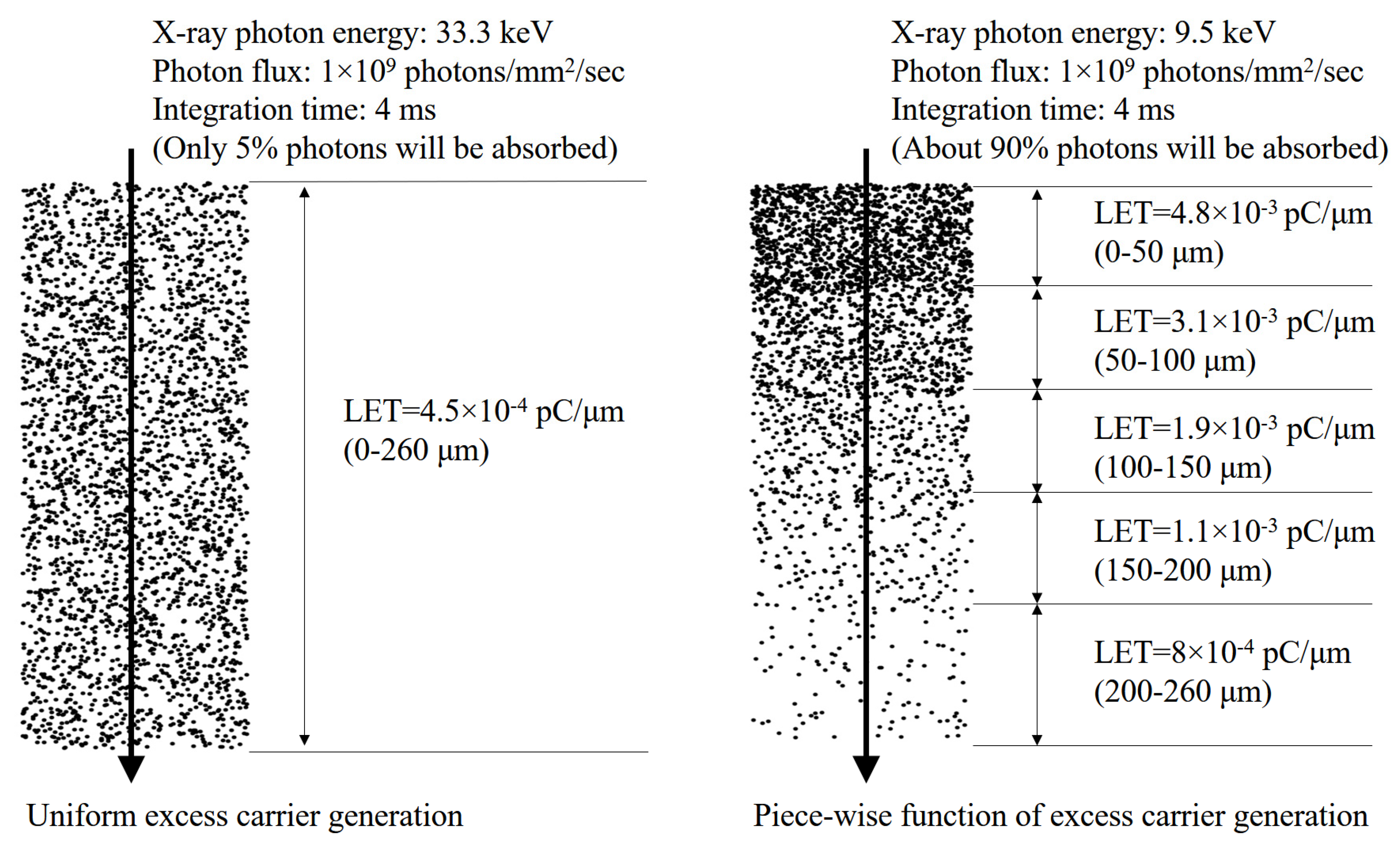
Figure 4.
Two-dimensional electric potential profile near the P+ node in Structure A (a) and in Structure B (b).
Figure 4.
Two-dimensional electric potential profile near the P+ node in Structure A (a) and in Structure B (b).

Figure 5.
Collection efficiency of Structure A (a) and Structure B (b) vs. d3 at different d1 and d2. The BPW ring has constant width of 3 μm. The X-ray photon energy is 33.3 keV.
Figure 5.
Collection efficiency of Structure A (a) and Structure B (b) vs. d3 at different d1 and d2. The BPW ring has constant width of 3 μm. The X-ray photon energy is 33.3 keV.

Figure 6.
Impact of BPW doping concentration on the collection efficiency of Structure A (a) and Structure B (b). The X-ray penetration location is at the center of the target pixel. d1 is the BPW width in Structure A. d2 is the separation distance between BPW ring and the pixel center in Structure B. The BPW ring has constant width of 3 μm.


Figure 7.
The impact of the X-ray photon energy on the collection efficiency of Structure A (a) and Structure B (b). In both Structure A and Structure B, higher collection efficiency can be observed with Ephoton = 9.5 keV.
Figure 7.
The impact of the X-ray photon energy on the collection efficiency of Structure A (a) and Structure B (b). In both Structure A and Structure B, higher collection efficiency can be observed with Ephoton = 9.5 keV.

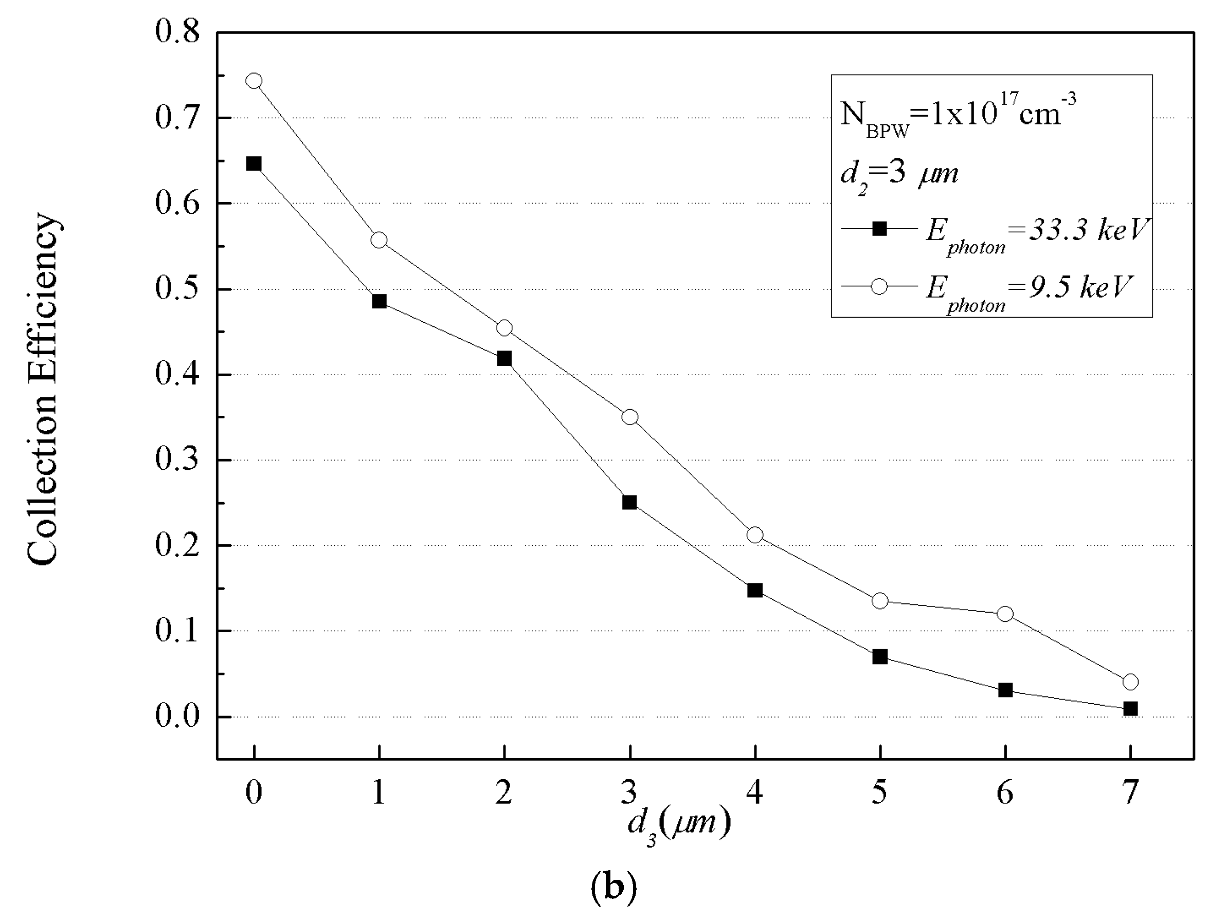
Figure 8.
The impact of the BPW doping concentration on the conversion gain for (a) Structure A and (b) Structure B. The X-ray penetration location is at the center of the target pixel. The BPW ring has a constant width of 3 μm.
Figure 8.
The impact of the BPW doping concentration on the conversion gain for (a) Structure A and (b) Structure B. The X-ray penetration location is at the center of the target pixel. The BPW ring has a constant width of 3 μm.

Table 1.
Description of two types of pixel structures.
| Structure | Explanation |
|---|---|
| Structure A: pixel with extended BPW | The width of the extended BPW is (2 × d1) μm |
| Structure B: pixel with a BPW ring | BPW ring needs other additional P+ nodes to fix its potential; the width of the ring is 3 μm and the width of these four P+ nodes is 1 μm; the separation between the P+ node and the BPW ring is d2 μm. |
© 2017 by the authors. Licensee MDPI, Basel, Switzerland. This article is an open access article distributed under the terms and conditions of the Creative Commons Attribution (CC BY) license (http://creativecommons.org/licenses/by/4.0/).
Share and Cite
MDPI and ACS Style
Shi, C.; Tian, L.; Feng, S.; Li, Q.; Wang, H. Design and optimization of collection efficiency and conversion gain of buried p-well SOI pixel X-ray detector. Electronics 2017, 6, 26. https://doi.org/10.3390/electronics6020026
AMA Style
Shi C, Tian L, Feng S, Li Q, Wang H. Design and optimization of collection efficiency and conversion gain of buried p-well SOI pixel X-ray detector. Electronics. 2017; 6(2):26. https://doi.org/10.3390/electronics6020026
Chicago/Turabian StyleShi, Chen, Li Tian, Songlin Feng, Qiliang Li, and Hui Wang. 2017. "Design and optimization of collection efficiency and conversion gain of buried p-well SOI pixel X-ray detector" Electronics 6, no. 2: 26. https://doi.org/10.3390/electronics6020026
Note that from the first issue of 2016, this journal uses article numbers instead of page numbers. See further details here.