3.1. 300-h Test
The devices showed a very apparent “burn-in” effect, with a rapid change in electrical characteristics followed by slow and more consistent (part-to-part) change. Due to this apparent burn-in effect, some of the following comparisons will treat the first post-stress characterization for the high-voltage-tested parts as the “initial” values; doing so is sufficient to remove the burn-in effect for all parts. Since the first post-stress characterization for the high-power-tested parts is also the last characterization for these devices, the pre-stress characterization will be treated as the initial values for the high-power-tested devices.
The nominal pre-stress conditions for the devices tested for 300 h follow: the average peak transconductance (gmp) was 201.2 mS/mm; the average threshold voltage was 2.88 volts; the average maximum drain current (IDmax) was 745.5 mA/mm; and the average maximum source current (ISmax) was 573.8 mA/mm.
Table 2 contains the changes at the end of the test period for each device. Most changes are listed as percentages, but the threshold voltage change is absolute. The initial values for the high-voltage-tested parts are from the 100-h characterization to remove the burn-in effect, as explained above. All devices trended as indicated by the signs in
Table 2. All devices exhibited a positive threshold voltage shift. The high-power conditions caused more change than the high-voltage conditions as seen in the greater magnitude changes shown in
Table 2.
To ensure that the positive gate biases used in some test conditions were not the cause of degradation, we subjected devices from the same family as reported herein to high forward gate bias (+6 V) and current (>1.8 A/mm) for >17.5 h. The HEMTs survived this condition and exhibited only a slight change in gate diode characteristic, little decrease in maximum drain current, with only a 0.1 V positive threshold voltage shift, and remarkably, a persisting breakdown voltage exceeding 200 V.
Our commercially purchased reliability test station monitored gate leakage current, but not with sufficient accuracy to provide any useful data for this research. While some reports show increased gate current after exceeding a “critical voltage” [
14], we tested two representative devices to the limits of our power supplies (
VD = +200 V,
VG = −100 V) and did not see any such “critical voltage” breakdown. Instead, the bias conditions used in this study were chosen because they represent realistic device operating conditions and they closely follow industry standard accelerated life test (ALT) methodologies where saturated RF power and DC saturated drain current are key metrics for assessing device performance and degradation [
15,
16].
While determining the physical cause of the observed degradation was not an objective of this paper, there are published mechanisms that could apply. Degradation due to hot electrons is discussed in [
17,
18]. A prominently reported degradation mechanism in GaN HEMTs is the physical alteration of the drain side of the gate after stress [
15,
17,
19,
20]. In [
21], we reported our observations of physical damage after stress.
Based on the averages of the parameter data presented in
Table 2, there appears to be a correlation between higher drain biases (when power dissipation and channel temperature are held constant) and greater degradation. Although the estimated channel temperatures were similar for the high power tests and separately for the high voltage tests, the average change for the four parameters generally increased in magnitude with drain voltage. For high-power Condition 3, the degradation was more than it was for the other two high-power conditions.
Using the averages of the activation energies presented in [
2,
3,
4]—2.09 eV—and the averages of each condition’s channel temperatures estimates in
Table 1, the acceleration factors from Equation (1) between the test conditions were calculated. The acceleration factors (AF) suggest that the devices tested at Condition 1 should have, based on the AF alone, degraded slightly more than the Condition 3 devices (AF = 1.19), and Condition 2 more than Condition 3 (AF = 1.72). However, we see in
Table 2 that Condition 3 degraded the fasted as would be expected for a positive degradation correlation with drain voltage. To be fair, Conditions 2 and 3 are more comparable to each other than Condition 1 since Conditions 2 and 3 experienced similar power dissipation; error in the estimate of the thermal resistance of the sub-micron-sized channel region will affect Conditions 2 and 3 in about the same way and still leave them comparable to each other. Still, we see that the degradation caused by the high-power electrical conditions overshadows the degradation that may be caused by temperature for Condition 3.
On the other hand, high-voltage Condition 5 may have had a channel temperature between 246 and 248 °C versus 245 °C for the channel temperature of the other high-voltage condition. This implies 1.09 < AF < 1.31 for Condition 5 versus Condition 4. As such, for the changes shown in
Table 2 for the high voltage tests, we do not rule out agreement with the expectations of the Arrhenius model.
Figure 1 shows the pre- and post-stress values of
IDmax and
IDSS, respectively, normalized to the pre-stress values for the high-power conditions. The plots of the Condition 1 and 2 drain currents overlap, indicating that these conditions had similar responses to their stresses, despite different drain voltage and power dissipation levels. The plots of the Condition 3 drain currents are distinctly separate from those of Conditions 1 and 2, despite the similar
Tch estimates for all three conditions and the same power dissipation as Condition 2. Condition 3 shows a marked difference to Conditions 1 and 2. In fact, ±15% ranges around Conditions 1 and 2 slope averages overlap each other, while the ±15% range around the Condition 3 average does not overlap the ±15% ranges of either Condition 1 or 2 averages.
A similar analysis of the slopes of the
IDmax and
IDSS lines can be performed for the high-voltage conditions.
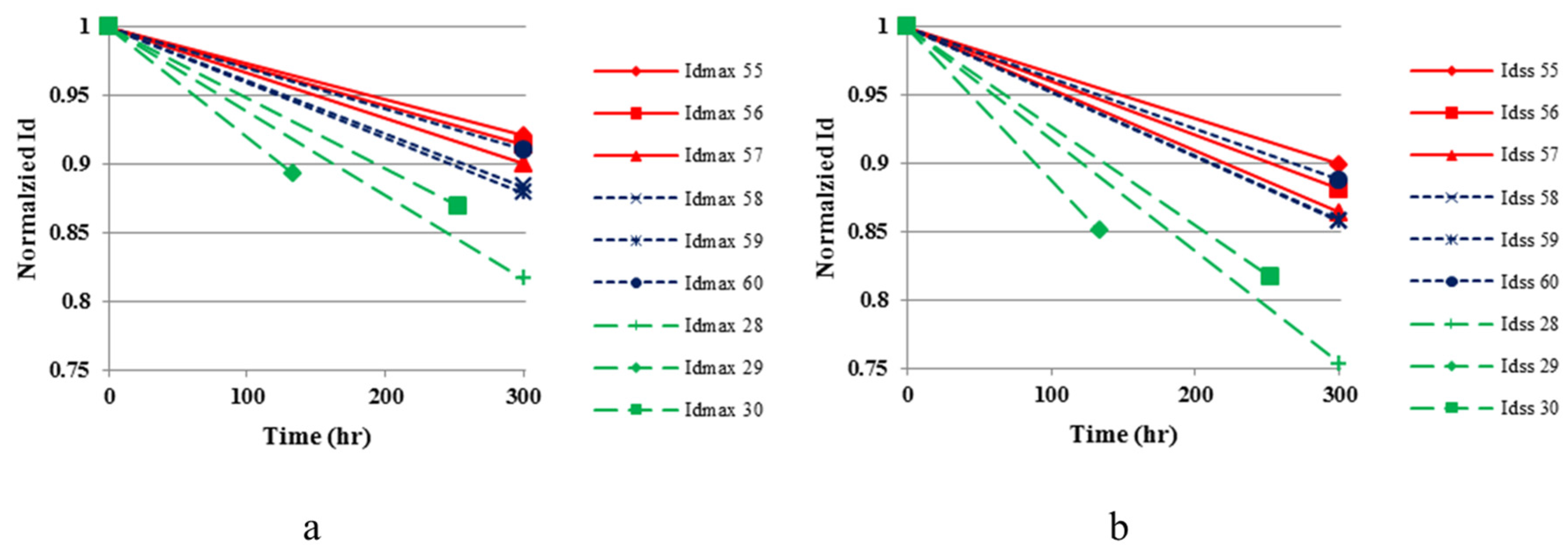
Figure 2 shows the pre- and post-stress values of
IDmax and
IDSS, respectively, normalized to the 100 h values. The plots of
IDmax overlap, and the Condition 5
IDSS lines encompass the Condition 4
IDSS lines, indicating that both conditions had similar responses to their stresses, despite different drain voltages. Ranges of ±15% around the Condition 4 and 5
IDSS linear-fit slope averages overlap, but ±15% ranges around the
IDmax linear-fit slope averages do not. Although the slope averages increase with drain voltage and the ±15%
IDmax slope average ranges do not overlap, the overlapping
IDmax and I
DSS plots indicate similar behavior for the high voltage test.
The following is an analysis of the sensitivity of the high power test to different sources of variation. To examine the effect of the test station on device degradation measurements, the initial parameters were first recorded.
Table 1 contains the values of parameters of interest at time 0 of the stress period as measured by the test station while at the stress base-plate temperature. There are multiple sources of measurement variation within the test station: ±2 °C for base-plate temperature, ±50 mV for drain voltage, and ±1.5 mA (equivalently 15 mA/mm) for drain current. In addition to the measurement variation, the setability accuracy for drain current is 1.5 mA, and base-plate temperature is ±2 °C. The drain current measurements (and calculated power dissipations) are the largest sources of variation in the channel temperature estimates in
Table 1 for the high-power conditions.
Assuming the initial measured values had persisted throughout the test, a correlation between the channel temperature estimates of
Table 1 and the degradation for each device (
Table 2) for the high-power conditions can be investigated. For comparison purposes, the high-power-tested device values are compared to nominal values of
Tch =395 °C (the average of the
Tch estimates in
Table 1), −2%
gmp, a Δ
VT of +300 mV, −10%
IDmax, and −10%
IDSS. With the nominal
Tch value as
T1 in Equation (1), acceleration factors are calculated to compare each high-power-tested device to the nominal values. This analysis indicates there is no correlation between the acceleration factors and the observed degradation, which means that the observed degradation was not caused by the variation in initial measured parameter values.
The following analysis investigates the initial
Tch estimates of
Table 1 and the measurement error from the Agilent power supplies during initial and final characterizations. Based on the Agilent specifications [
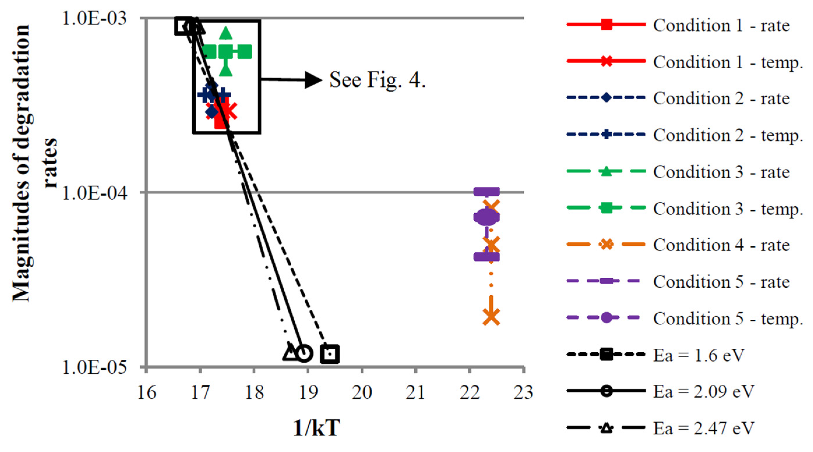
22], the drain current measurement error depends on the measured current value and the output voltage, which also has a measurement error dependent on the measured output voltage. The drain voltage measured 10 V and the error was ±7 mV. For the high-power-tested devices, the maximum drain current error for the initial characterizations was 0.108 mA, and, for the final characterizations, was 0.102 mA. The maximum drain current error for the initial and final characterizations of the high-voltage-tested devices was 0.107 mA. Degradation rates (linear-fit slopes from
Figure 2 and
Figure 3) are calculated from the initial and final
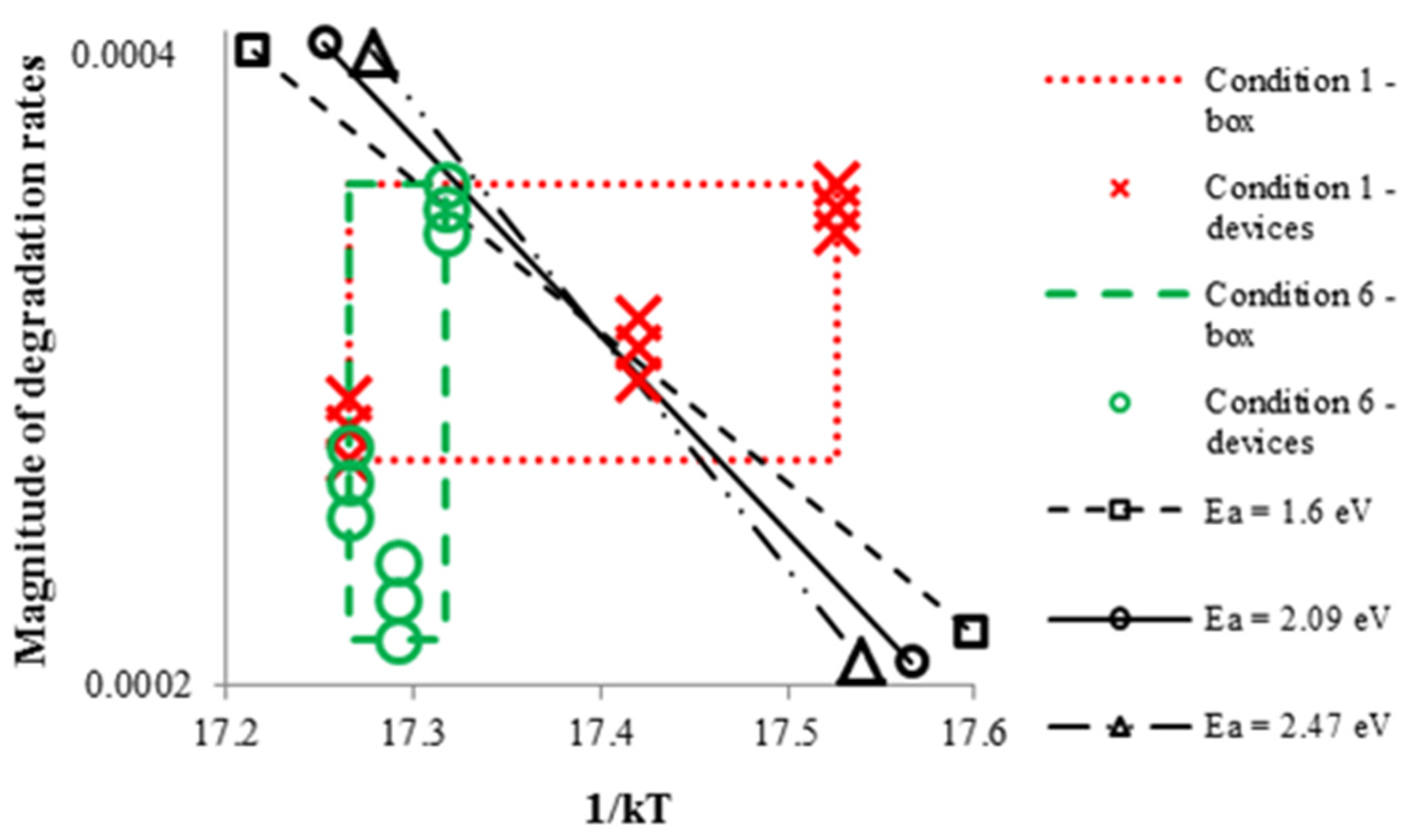
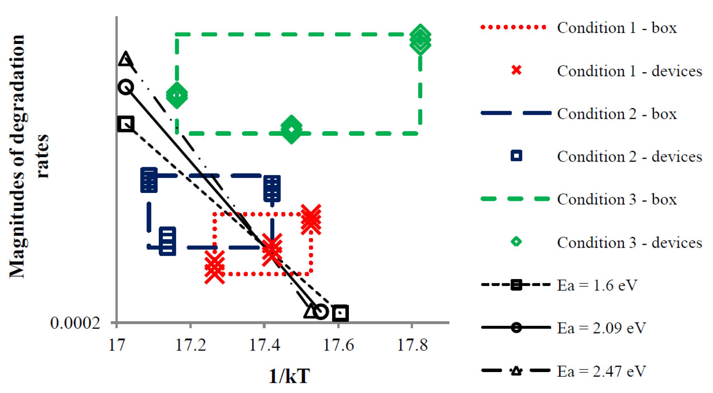
IDmax characterizations and times. Finally, the magnitudes of the degradation rates are plotted against the temperatures (1/kT) in
Figure 4. The center points are the average
Tch estimates and the average rates in a condition. The endpoints are the minimum and maximum rates along the line of average temperatures and the minimum and maximum
Tch estimates along the line of average rate in a condition. Conditions 4 and 5 have greater rate ranges since there was little difference between the initial and final drain current values, which resulted in the same maximum error of 0.107 mA. Also included in
Figure 3 are reference lines that pass through the center point of Condition 1 and assume activation energies of 2.09 (used previously in this paper), 1.6, and 2.47 eV (the range of values surveyed in [
5] that resulted from DC testing).
As can be seen from
Figure 3, Conditions 1 and 2, and separately 4 and 5, have overlapping ranges and are similar. Notice that the reference lines through Condition 1 do not approach Conditions 4 and 5. Conditions 4 and 5 appear related to each other by the Arrhenius model. Since the high power test results are clustered closely in
Figure 3, the portion of the graph containing these conditions is magnified in
Figure 4.
In
Figure 4, the error bars are replaced with error boxes, and individual device data are plotted. As seen in
Figure 4, the ranges of Condition 3 do not overlap those of Conditions 1 and 2, which suggests that Condition 3’s behavior may not have been caused by temperature, even with measurement error and variation of initial biases. However, the reference lines could be shifted to the right such that the lines intersect all three boxes, suggesting an Arrhenius relationship between the conditions. The inconsistency, though, is that Conditions 3’s box is up and to the right of Condition 1, when it should be down and to the right for its lower average
Tch estimate (see
Table 1).
Finally, an analysis of the sensitivity of Conditions 1, 2, and 3 to thermal resistance (
Rth) changes in the thermal model is investigated. The accuracy of any thermal resistance estimate for these devices is subject to significant error [
6,
7,
23], and it is an underappreciated fact that the sensitivity of conclusions drawn in an accelerated life test to the thermal resistance assumed should be considered [
7]. The analysis computes new
Tch estimates with [(
Tch −
Tbp) × (±20%)] +
Tbp for a ±20% change in thermal resistance. Then, acceleration factors between test conditions are calculated with the new
Tch estimates.
Table 3 lists the new
Tch estimates and acceleration factors (AF), as well as the original
Tch estimates and acceleration factors. The new AF’s generally indicate the same behavior as the original AF’s for Condition 2 versus 3: Condition 2 should degrade more than Condition 3. Depending on the error, though, Condition 1 may degrade much more or less than Conditions 2 and 3 based on AFs. Recall that the observed behavior was not what was indicated by the Arrhenius model—Condition 3 degraded more than Conditions 2 and 3.
Based on the foregoing data, the evidence indicates that temperature was not the cause of degradation in the high-power tested devices, especially, since there were significant differences in the responses of Conditions 2 and 3. From the sensitivity analysis, the variation of the test station bias setting and measurements in initial measured parameter values, the characterization measurement error, and the thermal resistance error in the thermal model are not sufficient to discount the differences in degradation or the conclusion that temperature did not cause the degradation. In contrast, for the high-voltage-tested parts, there is sufficient similarity and overlap in degradation values and plots to indicate that the observed changes may have been caused by temperature. Therefore, the Arrhenius model may be valid for some bias conditions, but not for others.
3.2. 600-h High-Power Test
Similar to the burn-in effect observed in the 300 h test above, the devices of the 600 h test showed a more rapid decrease in the first hour of stress than in subsequent hours. Consequently, the 1 h characterizations at 245 °C are considered to be the “initial” data points for the pre- and post-stress characterizations.
The nominal pre-stress conditions for the devices tested for 600 h follow: the average peak transconductance (
gmp) was 202.1 mS/mm; the average threshold voltage was −2.96 volts; the average maximum drain current (
IDmax) was 760 mA/mm; and the average maximum source current (
ISmax) was 591 mA/mm. The devices were from the same lot as the devices used for the 300-h test.
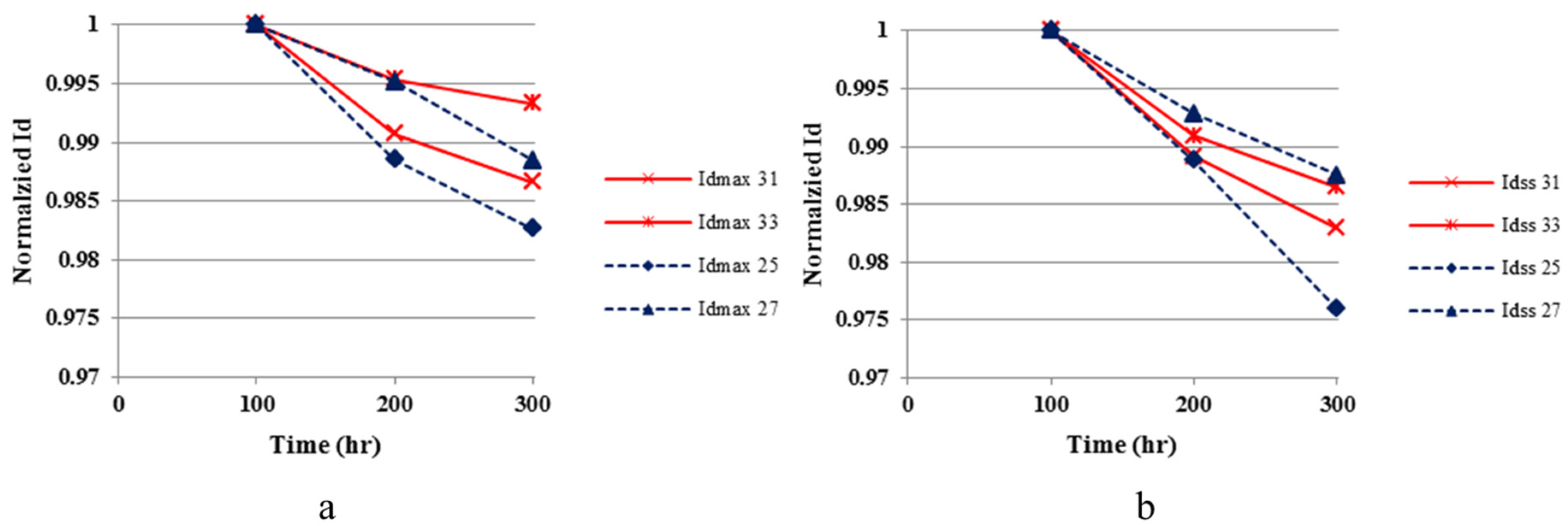
Table 4 contains the changes at the end of the 200 and 600 h for each device.
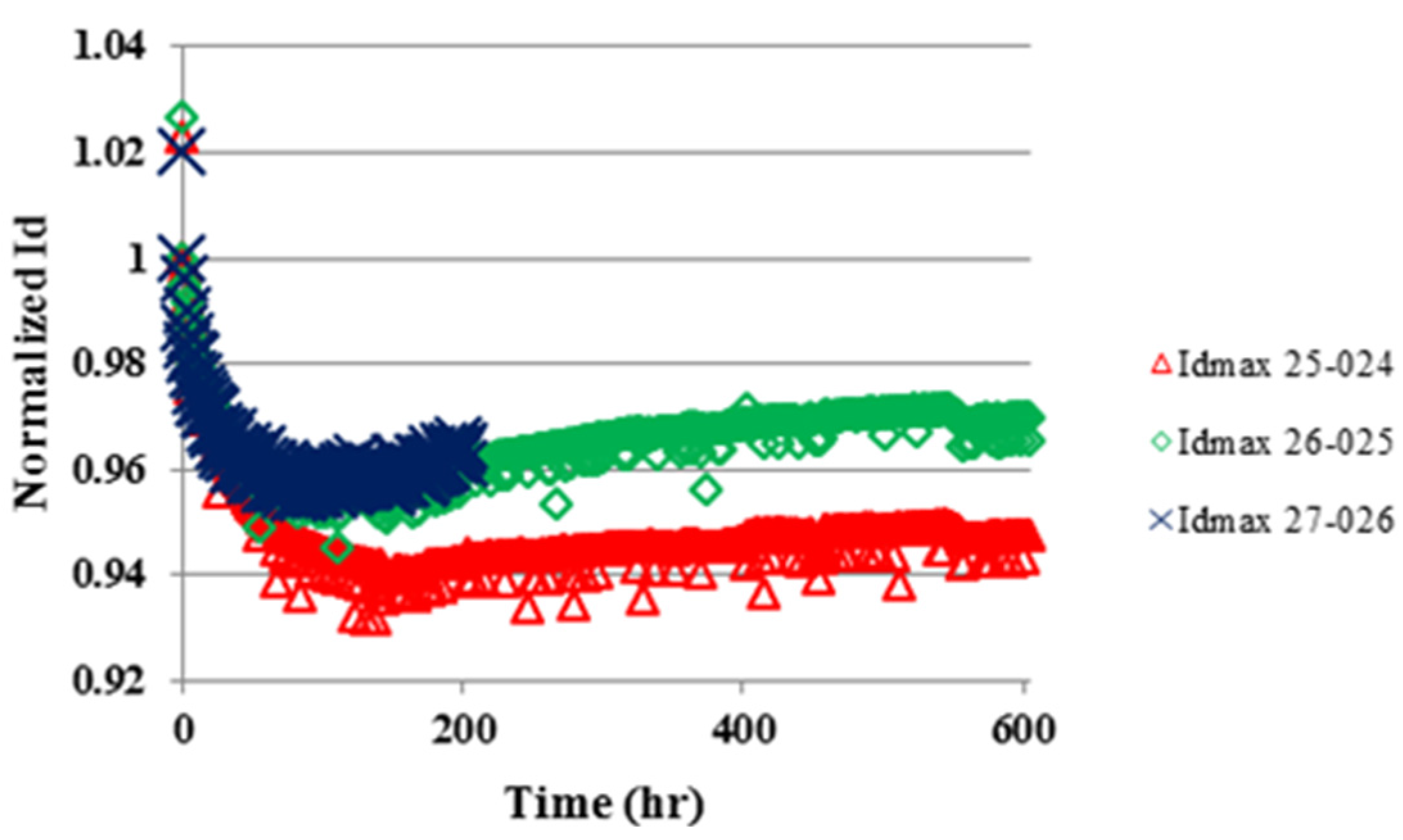
Figure 5 shows the normalized values (to the 1 h, 245 °C measurements) of
IDmax over time for the devices in the 600 h test. Interestingly, after initially degrading, the devices began to recover during stress. This recovery is evident in decreased magnitudes of averages, from 200 to 600 h, of the parameter data in
Table 4.
As with Conditions 2 and 3 of the 300 h test, Condition 1 of the 300 h test and Condition 6 of the 600 h test are comparable since they experience similar power dissipation. However, the
Tch estimate for Condition 6 is 405 °C, and the acceleration factor between Conditions 6 and 1 is 1.80, indicating that Condition 6 should be different than the other conditions. Therefore, Condition 6 was expected to degrade more than Condition 1.
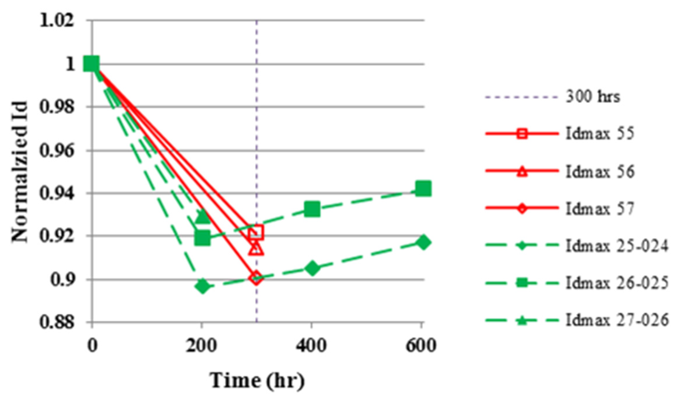
Figure 6 contains plots of the 70 °C characterization data for the 300-h and 600-h tests. As in
Figure 5, the drain current recovers in the 600-h test devices. Interpolating the 600-h test data at 300 h reveals that Condition 6, in fact, did not degrade more than Condition 1, contrary to Arrhenius expectations.
The following is a brief analysis of the sensitivity of Conditions 1 and 6 to the initial measured parameter values. To begin, the initial measured parameter values of Conditions 6 are listed.
Table 1 contains the values of parameters of interest at time 0 of the stress period as measured by the test station while at the stress base-plate temperature.
Then, the initial
Tch estimates for Conditions 1 and 6 in
Table 1 and the measurement error from the Agilent power supplies during the initial 300-h characterizations are analyzed in direct analogy to the analysis of
Figure 4 and
Figure 5. Linear interpolations of the 200 h and 400 characterizations of Devices 25-024 and 26-025 are used to obtain 300 h characterization estimates for these devices. A 300-h characterization estimate is extrapolated for Device 27-026 from its 200-h characterization using the average of the slopes calculated for the linear interpolations od Devices 25-024 and 26-025. Based on the Agilent specifications [
22], the error for the measured drain voltage of 10 V is ±7 mV. For Condition 1, the maximum drain current error for the initial characterizations is 0.108 mA, and for the 300-h characterizations is 0.102mA. For Condition 6, the maximum drain current error for the initial characterizations is 0.109 mA, and for the 300-h characterization estimates is 0.103 mA. Degradation rates are calculated from the initial and 300 h I
Dmax characterizations and times. Finally, the magnitudes of the degradation rates are plotted against the temperatures (1/
kT) in
Figure 7. The center points are the average
Tch estimates and the average rates in a condition. The endpoints are the minimum and maximum rates along the line of average temperature and the minimum and maximum
Tch estimates along the line of average rate in a condition.
As can be seen in
Figure 7, Conditions 1 and 6 have overlapping ranges and the reference lines could be moved left to intersect both boxes, indicating similar behavior. The initial
Tch estimates for Condition 6 are generally higher than those of Condition 1, yet the degradation rates are generally similar. The average initial
Tch estimates for Condition 6 is 398 °C, and the average initial
Tch estimates for Condition 1 is 394 °C. The Arrhenius acceleration factor between these average temperatures is 1.24. The inconsistency here with the Arrhenius model is that the Condition 6 box is down and to the left of the Condition 1 box, when it should be up and to the left for its higher average initial
Tch estimate.
3.3. Discussion
In the data presented, there are two instances where the Arrhenius model seems reasonable. These instances occur when GaN HEMTs were tested at a similar channel temperature estimates. These instances are between Conditions 1 and 2 and between Conditions 4 and 5 (although the average degradation for these conditions has a positive correlation to drain voltage).
Conversely, there are two instances of inconsistency with the Arrhenius model. Both instances occur when the test conditions are similar. One instance—between Conditions 2 and 3—occurs when similar degradation was expected, but the two conditions exhibited different degradation. The other instance—between Conditions 1 and 6—occurs when different behavior was expected, but similar behavior was observed. In addition, the error boxes of Conditions 3 and 6 are not where they are expected to be based on the Arrhenius relation.
Another instance of inconsistency is between the high-voltage conditions and the high-power conditions. Reference lines assuming activation energies do not intersect the error regions of the two different sets of conditions (see
Figure 3). This inconsistency indicates that GaN HEMT degradation depends on the test conditions.
The average points of all the test conditions follow a positive correlation to drain bias. For the high-voltage conditions, the average degradation rate is higher for Condition 5 (
VDS = 100 V) than for Condition 4 (
VDS = 60 V). For the high-power conditions, the progression from lowest to highest average degradation rate is Condition 6 (
VDS = 17.5 V), Condition 1 (
VDS = 20 V), Condition 2 (
VDS = 40 V), and Condition 3 (
VDS = 60V) (see
Figure 3,
Figure 4 and
Figure 7).
Reliability evaluation of aluminum gallium nitride (AlGaN)/GaN HEMT’s will benefit from considering other accelerants besides temperature. Based on the observations from this study, drain bias showed a positive correlation to degradation in a high-power test condition. Voltage acceleration would be a primary additional accelerant to pursue. To adequately consider other accelerants, the design of experiment methodology could be applied to create the multi-variable tests. Then, multi-stress models could be used in place of the single-stress Arrhenius model to analyze the data. Possible multi-stress models to use include the Generalized Eyring model [
12] Generalized Log-Linear relationship, and the Proportional Hazards model [
24]. Each model allows more than two stressors to be applied as accelerants.
Reliability assessments that employ more and different accelerants than temperature will result in more accurate lifetime estimates of AlGaN/GaN HEMTs since they will account for the failure mechanisms of the electrothermomechanical system that are not primarily thermally activated. For example, if a temperature-accelerated life test was conducted near Conditions 1 and 2, but device operation occurred near Condition 3, the Arrhenius extrapolations would be optimistic.
Based on this study, and [
9,
10], the need for different accelerants when assessing GaN HEMT reliability is shown. Additionally, [
14,
19,
20] investigated the effect of increasing drain-to-gate voltage
IDmax. They observed that higher drain-to-gate voltages degraded drain current, especially after a “critical voltage”. These authors showed, in effect, that GaN HEMT degradation for some devices could be accelerated with voltage. In contrast to [
14,
19,
20], our devices required high voltage in conjunction with power dissipation for degradation; higher voltages without power did not cause similar degradation. Similar devices to ours from the same vendor, tested independently, behaved similarly without degradation according to the inverse piezoelectric effect, as expected by the “critical voltage” model [
25,
26].


