Article

Simulation of 50-nm Gate Graphene Nanoribbon Transistors

Institut für Mikro-und Nanoelektronik, Technische Universität Ilmenau, PF 100565, 98684 Ilmenau, Germany
*
Author to whom correspondence should be addressed.
Electronics 2016, 5(1), 3; https://doi.org/10.3390/electronics5010003
Submission received: 2 November 2015 / Revised: 22 December 2015 / Accepted: 29 December 2015 / Published: 12 January 2016
(This article belongs to the Special Issue Two-Dimensional Electronics - Prospects and Challenges)

Abstract

:
An approach to simulate the steady-state and small-signal behavior of GNR MOSFETs (graphene nanoribbon metal-semiconductor-oxide field-effect transistor) is presented. GNR material parameters and a method to account for the density of states of one-dimensional systems like GNRs are implemented in a commercial device simulator. This modified tool is used to calculate the current-voltage characteristics as well the cutoff frequency fT and the maximum frequency of oscillation fmax of GNR MOSFETs. Exemplarily, we consider 50-nm gate GNR MOSFETs with N = 7 armchair GNR channels and examine two transistor configurations. The first configuration is a simplified MOSFET structure with a single GNR channel as usually studied by other groups. Furthermore, and for the first time in the literature, we study in detail a transistor structure with multiple parallel GNR channels and interribbon gates. It is shown that the calculated fT of GNR MOSFETs is significantly lower than that of GFETs (FET with gapless large-area graphene channel) with comparable gate length due to the mobility degradation in GNRs. On the other hand, GNR MOSFETs show much higher fmax compared to experimental GFETs due the semiconducting nature of the GNR channels and the resulting better saturation of the drain current. Finally, it is shown that the gate control in FETs with multiple parallel GNR channels is improved while the cutoff frequency is degraded compared to single-channel GNR MOSFETs due to parasitic capacitances of the interribbon gates.

Graphical Abstract

1. Introduction

The 2D (two-dimensional) carbon-based material graphene has attracted significant attention during the past 10 years [1]. During the early years of graphene research, i.e., in the period 2004–2009, particularly the high carrier mobilities observed in large-area graphene raised expectations that graphene could be an excellent channel material for future MOSFET (metal-oxide-semiconductor field-effect transistor) generations. Unfortunately, large-area graphene as the natural form of appearance of graphene does not possess a bandgap. Thus, MOSFETs with large-area graphene channels (designated as GFETs in the following) do not switch off and cannot be used for digital logic. RF (radio frequency) FETs, on the other hand, do not necessarily need to be switched off. Therefore a lot of work has been done to develop GFETs for RF applications and indeed experimental GFETs with cutoff frequencies fT in excess of 300 GHz have been reported [2,3,4]. Due to the missing gap, however, GFETs suffer from an unsatisfying saturation of the drain current causing poor power gain and low maximum frequency of oscillation fmax [5,6]. This seriously limits the potential of GFETs for high-performance RF applications. Thus, for both logic and high-performance RF FETs, a semiconducting channel is needed.
There are different options to open a gap in graphene, i.e., to make this material semiconducting. First, it has been shown that by using bilayer graphene instead of single-layer material and applying a perpendicular field, a gap is formed [7,8]. A second option is to create narrow confined graphene structures, such as GNRs (graphene nanoribbon) [9,10] or graphene nanomeshes [11,12], in which a gap opens. In the present work, we focus on GNRs and use these as MOSFET channels. The gap opening in GNRs has been predicted by first-principle calculations [13,14,15] and confirmed by experiments [9,10]. Meanwhile the International Technology Roadmap for Semiconductors considers GNRs as a viable channel replacement material for future MOSFET generations [16]. Recently back-gate GNR MOSFETs with ribbon widths down to 2 nm showing excellent switch-off and on-off ratios in excess of 106 have been demonstrated [17,18,19] and top-gate GNR MOSFETs with 10 to 20-nm wide channels and on-off ratios around 70 [20] have been reported.
On the theoretical side, GNR MOSFETs have been simulated at different levels of complexity and physics involved. Steady-state quantum simulations based on the NEGF (nonequilibrium Green’s function) approach assuming ballistic transport have been performed [21,22,23,24,25] and GNR MOSFET simulations taking edge scattering [26,27] and phonon scattering [25] into account have been conducted. Moreover, the RF performance of GNR MOSFETs has been investigated by numerical simulations [21,22,25] and analytical equations have been developed to calculate the steady-state behavior and the RF properties of GNR MOSFETs [28].
While these simulations have provided valuable insights in the operation and physics of GNR MOSFETs, so far only simplified transistor structures with a single GNR channel and, in many cases, idealized conditions such as ballistic carrier transport have been considered. This has led to overly optimistic performance predictions such as unrealistically high simulated cutoff frequencies [21,22,25,28]. Moreover, most simulations have been performed using in-house tools not accessible by the community. An exception worth mentioning is the open-source multiscale simulation framework for the investigation of nanoscale devices such as GNR MOSFETs presented in [29]. However, commercial device simulators which are very popular in the semiconductor industry so far have not been applied to the investigation of GNR MOSFETs.
In the present work, we develop an approach to describe the steady-state and RF behavior of GNR MOSFETs in the framework of a commercial device simulator. Since so far neither graphene nor GNR models are implemented in commercial tools, in Section 2 the GNR models we have implemented in the device simulator ATLAS [30] are described and an approach to appropriately account for the DOS (density of states) and quantum capacitance of 1D (one-dimensional) systems such as GNRs in commercial simulation tools is presented. Section 3 summarizes the results of our ATLAS simulations, first for a simplified single-channel GNR MOSFET structure with 50 nm gate length and next for GNR MOSFETs with multiple parallel GNR channels and interribbon gates. Such multiple-channel GNR MOSFETs are studied here for the first time in detail. Finally, Section 4 concludes the paper.

2. Simulation Framework and GNR Models

Appropriate models for the material and carrier transport parameters for GNRs and a formalism to correctly account for the DOS in 1D structures are still missing in ATLAS. Therefore, the first steps of our work are (i) the compilation of data for the material and transport parameters needed for the simulation of GNR MOSFETs; (ii) the elaboration of a suitable approach to describe the DOS and the quantum capacitance in 1D GNR MOS structures properly; and (iii) the implementation of these features in ATLAS.

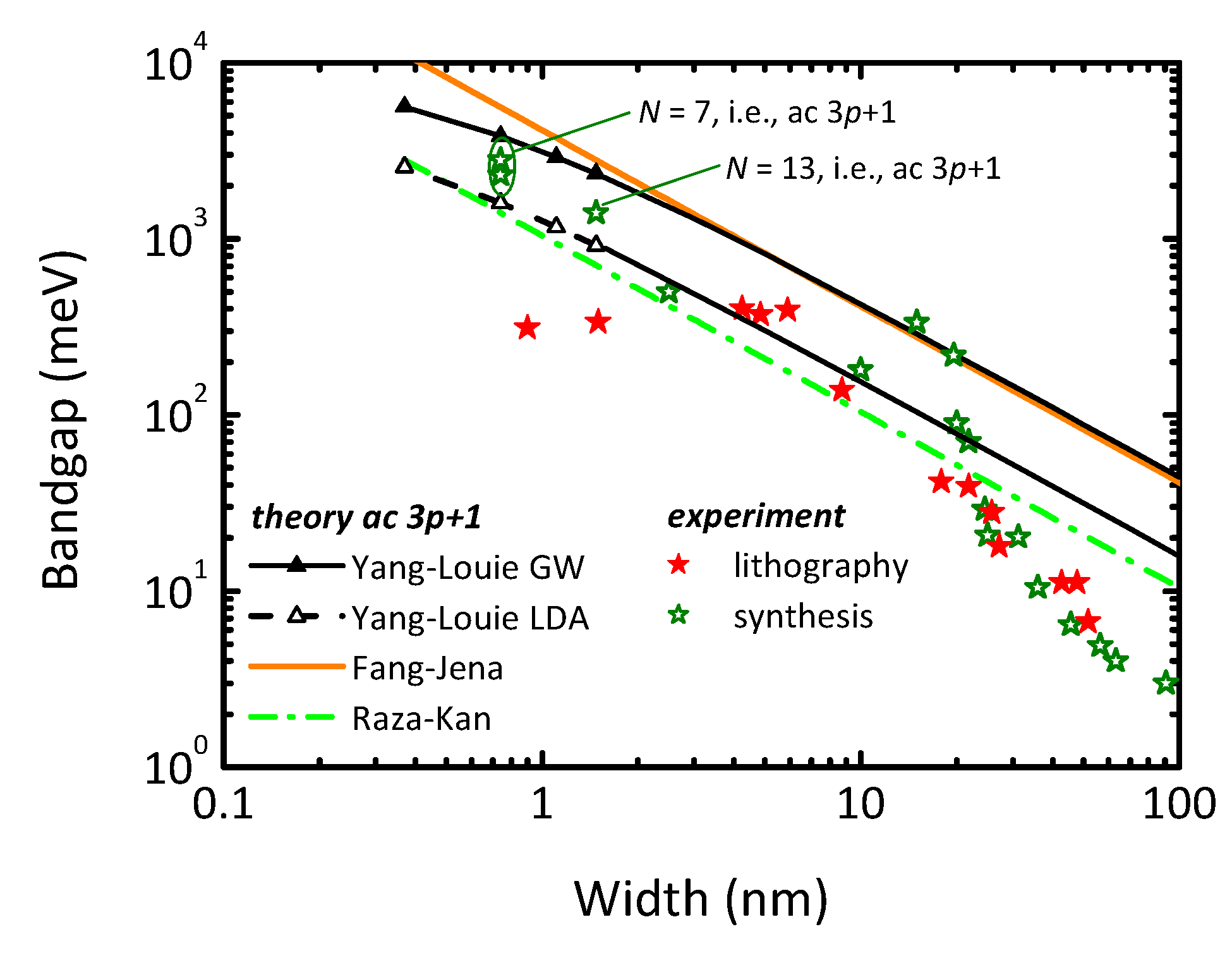
2.1. Models for Bangap and Carrier Effective Mass

It is well established that in narrow GNRs a sizeable bandgap can be opened and that the gap EG critically depends on the GNR edge configuration, i.e., ac (armchair) or zz (zigzag), and on the ribbon width w. GNRs of the ac configuration constitute the three different families 3p, 3p + 1, and 3p + 2 (p is an integer). For example, for a GNR with N = 7 carbon atoms along its width, p equals 2 and the ribbon belongs to the 3p + 1 family. Every family of ac GNRs obeys a specific gap-width relationship [4,13,14,15,31]. On the other hand, there is still a controversial debate on whether zz GNRs are metallic or semiconducting. In the present work, we exemplarily consider ac 3p + 1 GNRs and focus on the simulation of MOSFETs with N = 7 GNR channels.
The bandgap data for ac GNRs available in the literature consistently show for each family a decreasing gap for increasing ribbon width. For a given p, the gap obeys the relation EG(3p + 1) > EG(3p) > EG(3p + 2). However, as shown in Figure 1, the published EG-w data scatter considerably. This makes it difficult to develop a reliable EG-w model needed for device simulation. Obviously the reported experimental bandgap data points for the narrow N = 7 and N = 13 GNRs are located in between the results of the GW simulations of Yang et al. [14] and the predictions of Raza and Kan [13]. Moreover, most experimental bandgaps for GNR with widths from below 1 nm to about 20 nm are located in the range between these two predictions.
Figure 1. Measured and calculated bandgap of ac GNRs (graphene nanoribbon) vs. ribbon width. The experimental data for the N = 7 and N = 13 ac GNRs are taken from [10,32,33] and the other experimental data are taken from the compilation in [31]. The calculated bandgaps are taken from [13,14,34].
Electronics 05 00003 g001
In the present work, we use the EG-w relation from [13], which for the 3p + 1 family reads as
E G = 1.04 e V / w ( n m )
with
w ( n m ) = 0.246 2 ( N 1 )
Not only the bandgap but also the carrier effective mass meff in GNRs depends on the GNR edge configuration, family, and width. For ac GNRs of the 3p + 1 family, Raza and Kan suggested the expression [13]
m eff = 0.16 m 0 w
where m0 is the electron rest mass and w is the ribbon, according to Equation (2), in nm. The 3p + 1 family has been chosen in the present work since it provides, for a given p, the widest gap of the three families. We note, however, that our approach can be applied to the other two families of ac GNRs as well.

2.2. Transport Model

In the present work, carrier transport is described in the framework of the classical DD (drift-diffusion) model. It is frequently argued that in MOSFETs with sub-100-nm gates the DD model does no longer provide a sufficiently correct description of carrier transport due to the appearance of nonstationary and/or quasi-ballistic transport effects. We have demonstrated, however, that the standard DD model is well suited for the simulation of Si MOSFETs with gate length down to 30 nm, and by assuming a modified gate-length-dependent saturation velocity it provides reasonable results even down to 5 nm gate length [35]. Moreover, it has been shown that carrier transport in 2D MoS2 MOSFETs with 10-nm, and even sub-10-nm, channels is still far from ballistic but dissipative and scattering-dominated instead [36,37,38]. Finally, the DD approach is considered a reasonable guide even in the presence of nonstationary and quasi-ballistic transport in short-channel MOSFETs since it correctly accounts for both device geometry and electrostatics [39].
For a proper description of carrier transport in the DD model, the v-E (velocity-field) characteristics including the low-field mobility µ0, the high-field saturation velocity vsat, and the abruptness of the transition between the low-field and high-field regions have to be modeled correctly. The dependence of the effective mass on the ribbon width is already an indication of the fact that the properties of carrier transport in GNRs are related to the ribbon width. This has been confirmed by Monte Carlo transport simulations for 1.12, 2.62, and 4.86 nm wide ac ribbons belonging to the 3p + 1 family [40]. In the present work, we assume a Caughey–Thomas-type v-E characteristics with soft velocity saturation according to [41]
v = µ 0 E [ 1 + ( µ 0 E v sat ) β ] 1 / β
the v-E characteristics of the three GNRs reported in [40], and the parameters µ0, vsat, and β, see Table 1, are obtained by fitting.
Table 1. Parameters for the Caughey–Thomas fit of the v-E characteristics for three ac 3p + 1 graphene nanoribbons.
w (nm)µ0 (cm2/Vs)vsat (107 cm/s)βRemark
1.124602.21.4This work
2.6227003.21.3[40]
4.8612,0003.31.3[40]
Note that the N = 7, w = 0.74 nm GNR considered in the present work is outside the width range covered by the GNRs in Table 1. Therefore we extrapolate the trends for the parameters from Table 1 towards smaller widths and obtain µ0 = 195 cm2/Vs, vsat = 1.83 × 107 cm/s, and β = 1.4 for N = 7 GNRs.

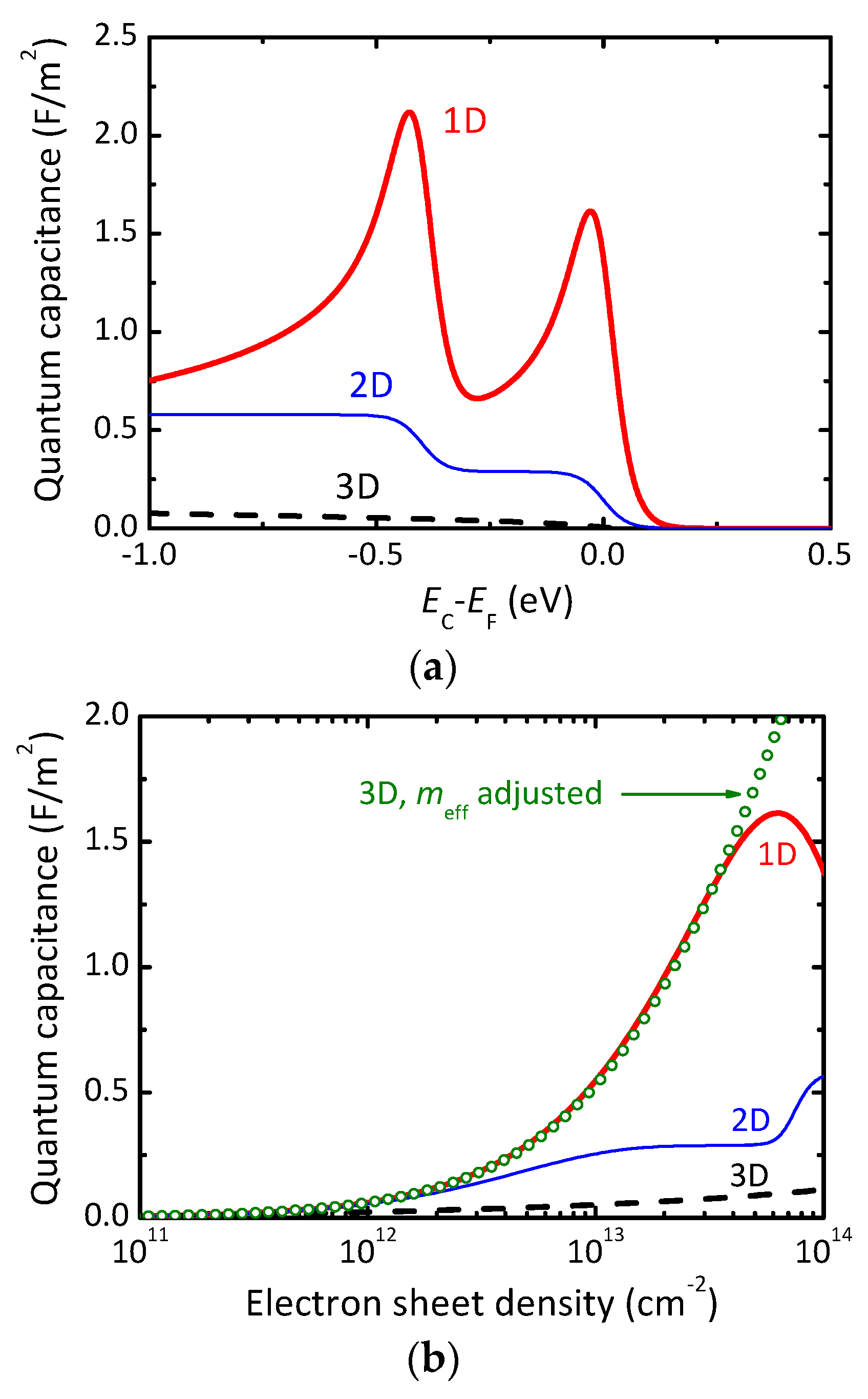
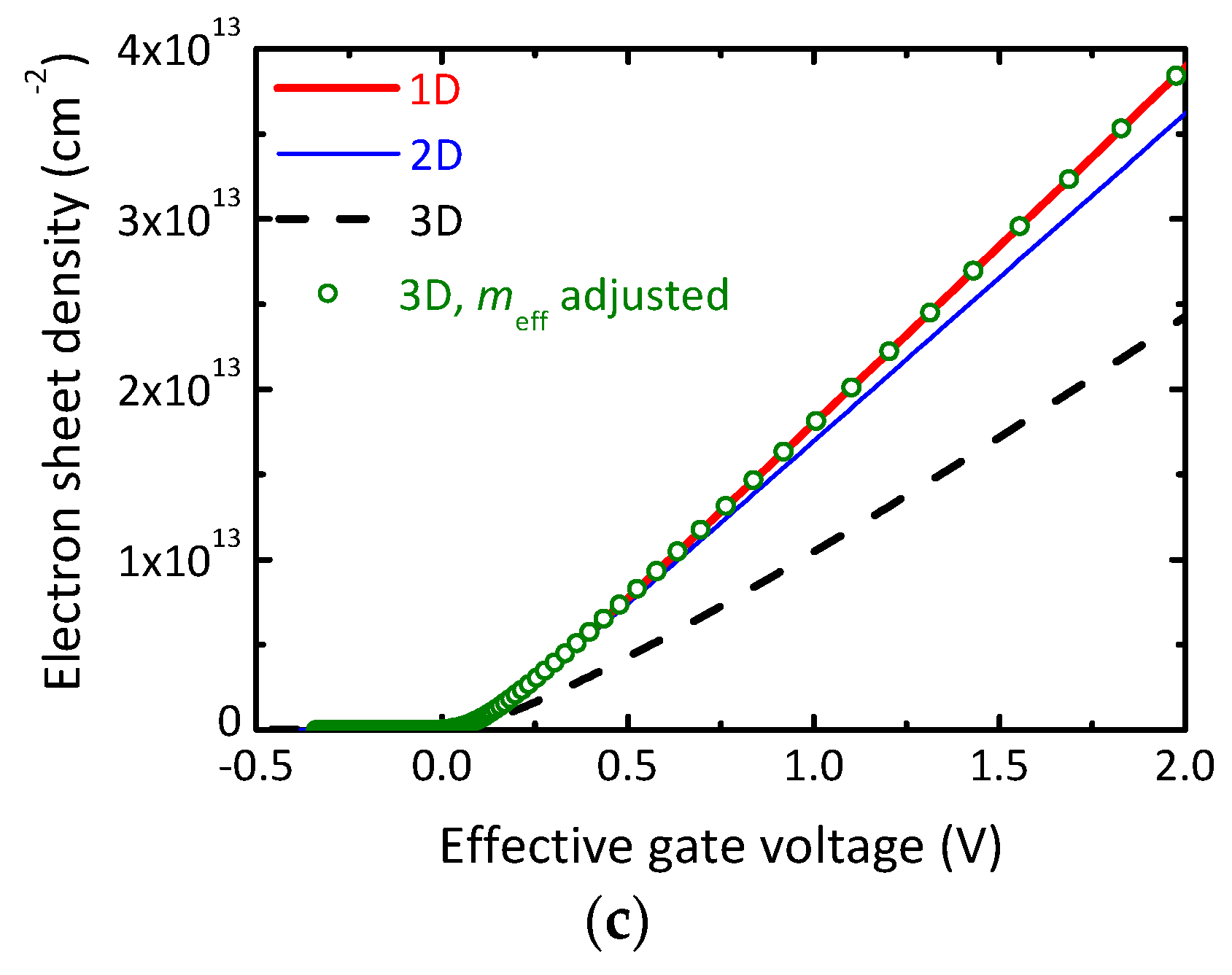
2.3. Modeling the Density of States and Quantum Capacitance of 1D Systems

To describe the gate control and electrostatics in low-dimensional MOS systems correctly, it is mandatory to model the DOS (density of states) and the gate capacitance CG accurately. In general, the gate capacitance of a MOS structure (regardless of the dimensionality of the channel) consists of a combination of the three capacitance components Cox, Ces, and Cq connected in series. Note that in the following we do not consider the absolute capacitance but the capacitance per unit area. Cox is the oxide capacitance given by Cox = εox/tox where εox is the dielectric constant and tox the thickness of the gate oxide; Ces is the electrostatic capacitance of the channel related to the average distance of the carriers from the oxide-channel interface; and Cq is the quantum capacitance of the channel related to the finite DOS of the channel. The simulator ATLAS (as most conventional device simulators) per se considers all semiconducting device regions (and thus the GNR channel of a GNR MOSFET) as a 3D material. Quantization effects occurring in the 2D system of a conventional MOS inversion channel can be taken into account by using quantum correction models implemented in ATLAS, while appropriate models for 1D systems, such as GNRs, are not yet available in commercial device simulators. On the other hand, the DOS of 1D systems differs significantly from that of 3D and 2D systems. If this is neglected in device simulations, the quantum capacitance may be dramatically underestimated leading to an undervalued gate control in 1D channels, particularly in GNR MOSFETs with thin gate oxide. Therefore, in the following we present an approach to emulate the effects of the 1D DOS of GNRs on the quantum capacitance and on the carrier density in the channel in the framework of ATLAS. In [42], we have elaborated physically correct analytical expressions for the carrier sheet density and the quantum capacitance in 1D systems. The corresponding equations, together with those for 2D and 3D systems, can be found in the Appendix.
Figure 2a shows the quantum capacitance of a N = 7 GNR as a function of the relative position of the Fermi level, i.e., ECEF where EC is the conduction band edge and EF is the Fermi level, calculated using the expressions from the Appendix for the 1D–3D cases. We have, as in all simulations in the present work, taken the first two subbands with a subband separation of 0.4 eV [43] into account, assumed GNRs with n-type conductivity, modeled the residual electron concentration by assuming a homogeneous n-type doping of the GNR of 2 × 1020 cm−3 which corresponds to an electron sheet density of 7 × 1012 cm−2, and used a relative dielectric constant of 1.8 for the GNR. It can be seen from Figure 2a that the quantum capacitance for the 1D case can easily exceed Cq assuming 3D conditions by one order of magnitude due to the huge qualitative and quantitative differences between the 1D and 3D densities of state.
Figure 2. (a) Quantum capacitance of a N = 7 ac GNR (graphene nanoribbon) channel vs. Fermi level position assuming a 1D, 2D, and 3D density of states. (b) Quantum capacitance of the corresponding GNR MOS structure with 1 nm equivalent oxide thickness and a gate metal work function equal to the GNR electron affinity. (c) Electron sheet density of the GNR MOS structure from (b) vs. effective gate voltage.
Electronics 05 00003 g002aElectronics 05 00003 g002b
Since the density of states depends on the carrier effective mass meff, a proper adjustment of meff in the expressions for the sheet density and quantum capacitance for the 3D case should, at least within a reasonably wide (ECEF) range, lead to a proper reproduction of the 1D quantum capacitance. Figure 2b shows the quantum capacitance for the 1D–3D cases calculated with the expression from the Appendix (now as a function of the electron sheet density), together with a second curve for the 3D case where we have used an adjusted effective mass, namely 24 times as large as the effective mass for the N = 7 GNR according to Equation (3). It can be seen that by using this modified effective mass, the quantum capacitance for the 3D case, i.e., the case handled by ATLAS, reproduces the quantum capacitance obtained from the correct equations for the 1D case almost perfectly for sheet densities up to 4 × 1013 cm−3.
Finally, Figure 2c shows the electron sheet density nsh versus the effective gate voltage VG-eff = VGVTh, where VG is the applied gate voltage and VTh is the threshold voltage defined as the gate voltage at which the electron sheet density nsh equals 3 × 1010 cm−2. It can be seen that nsh calculated for the 3D case is almost 40% lower compared to that for the 1D case. On the other hand, considering the 3D case and using the adjusted effective mass meff-adj = 24 × meff, the sheet density for the 1D case is perfectly reproduced over the entire gate voltage range considered. This brings us to the conclusion that using the expressions for the 3D case and assuming an adjusted carrier effective mass is an appropriate means to account for the specifics of the DOS of 1D systems properly. Therefore, in the ATLAS simulations to be discussed in the remainder of the paper, we always use the modified effective mass.

3. Simulated Transistor Structures, Simulation Results, and Discussion

To describe the behavior of GNR MOSFETs properly, actually 3D device simulations should be performed. Note that here the term 3D means that the GNR MOSFET by nature is a 3D device similar as the tri-gate MOSFET or the FinFET and that therefore in the simulation process the semiconductor equations (Poisson, current, and continuity equations) should be solved in three spatial dimensions. This should not be confused with the 3D case mentioned in Section 2.3. Since 3D simulations are computationally more expensive and sometimes more critical regarding convergence, we simulate the 2D GNR MOSFET structure shown in Figure 3 and initially consider only the effect of the top-gate on the channel and the electrostatics. The results of this study are presented in Section 3.1. In Section 3.2, we additionally consider the effect of interribbon gates on the operation of GNR MOSFETs with multiple parallel GNR channels.
Figure 3. Cross-section (in the x-y plane) of the simulated graphene nanoribbon MOSFET.
Electronics 05 00003 g003

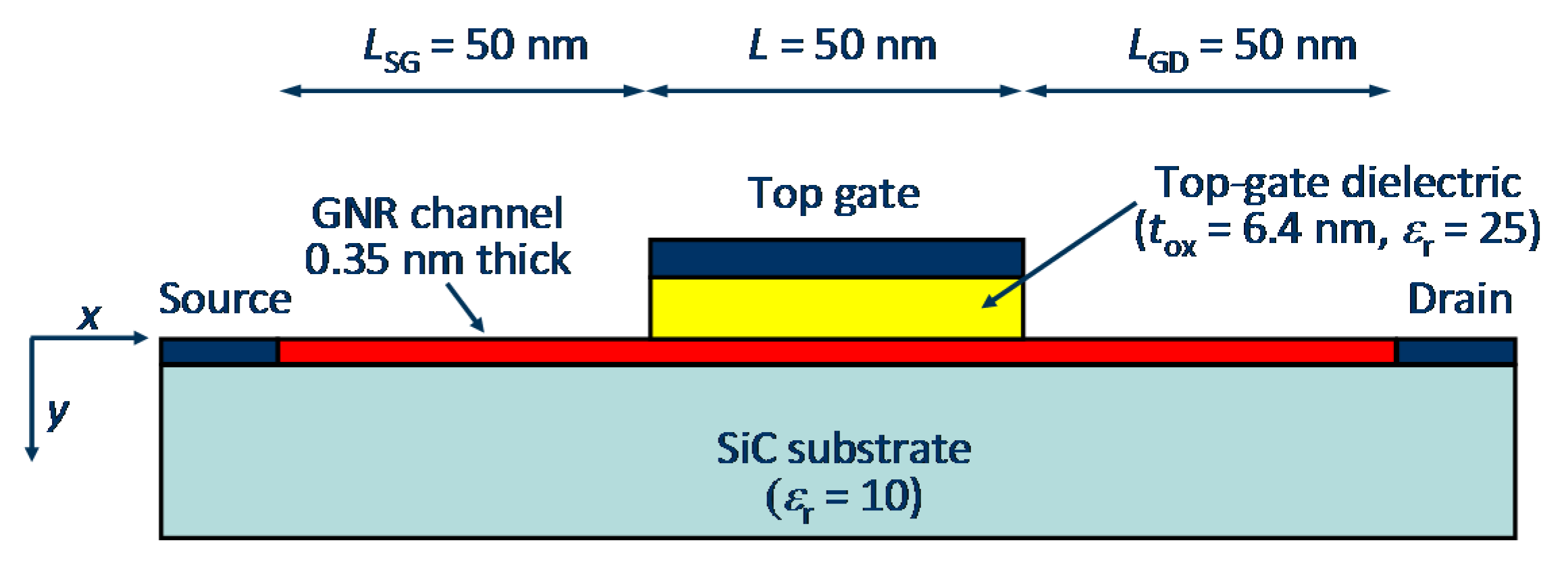
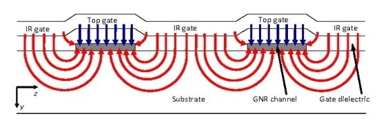
3.1. Simulated Transistor Structures

The basic structure of our simulated GNR MOSFETs is shown in Figure 3 in a cross-sectional view. The current flows in the x direction, the width of the GNR extends into the z direction (not shown), and the thicknesses of the substrate, the GNR channel, and the gate dielectric extend into the y direction. The structure consists of a semi-insulating SiC substrate, of which the upper part with a thickness of 1 µm is taken into account in the simulation.
On top of the substrate, an epitaxial GNR channel consisting of a N = 7 ac GNR with a thickness of 0.35 nm is located. The GNR is assumed to possess ideal ohmic source and drain contacts at its left and right ends and the top-gate dielectric is formed by a 6.4 nm thick HfO2 layer with a relative dielectric constant 25. This corresponds to an equivalent oxide thickness EOT of 1 nm. The gate has a length L of 50 nm and a work function equal to the electron affinity of the GNR, and the source-gate and gate-drain separations are 50 nm. Two layout configurations of the GNR MOSFET from Figure 3 are considered in the following. The first one is the single-channel transistor depicted in Figure 4a showing the cross-section in the y-z plane and in Figure 4b showing its top view. This configuration has only a top gate and no interribbon gate and for its investigation 2D device simulations are sufficient. We note that such single-channel devices have been considered in most previous theoretical investigations of GNR MOSFETs [21,22,23,24,25,26,27].
As has been shown in Figure 1, GNR channels with sufficiently wide bandgap are very narrow and therefore show only a limited current driving capability. To increase the transistor's drain current and to achieve the required current drivability, structures with multiple parallel GNR channels have to be used. The multiple-channel GNR MOSFET shown in Figure 4c,d constitutes the second configuration investigated in our study. The gate stripe of such a transistor consists of portions acting as the actual gate directly above the GNRs, i.e., the top gate, and of portions called interribbon gate located (on top of the HfO2 dielectric) between the parallel GNR channels. The control effect of the top gate is indicated by the straight black arrows in Figure 4a,c and the effect of the interribbon gates is indicated by the curved red arrows in Figure 4c.
Figure 4. Cross section and top view of a single-channel GNR MOSFET with top gate only and of a multiple-channel GNR MOSFET with interribbon gate. (a) Cross section of a single-channel GNR MOSFET in the y-z plane. (b) Top view of the single-channel GNR MOSFET from (a). (c) Cross section of a multiple-channel MOSFET with two parallel GNR channels and IR (interribbon) gate in the y-z plane. (d) Top view of the multiple-channel GNR MOSFET from (c). Note that in Figure 4a,c the current flows perpendicular to the paper plane.
Electronics 05 00003 g004

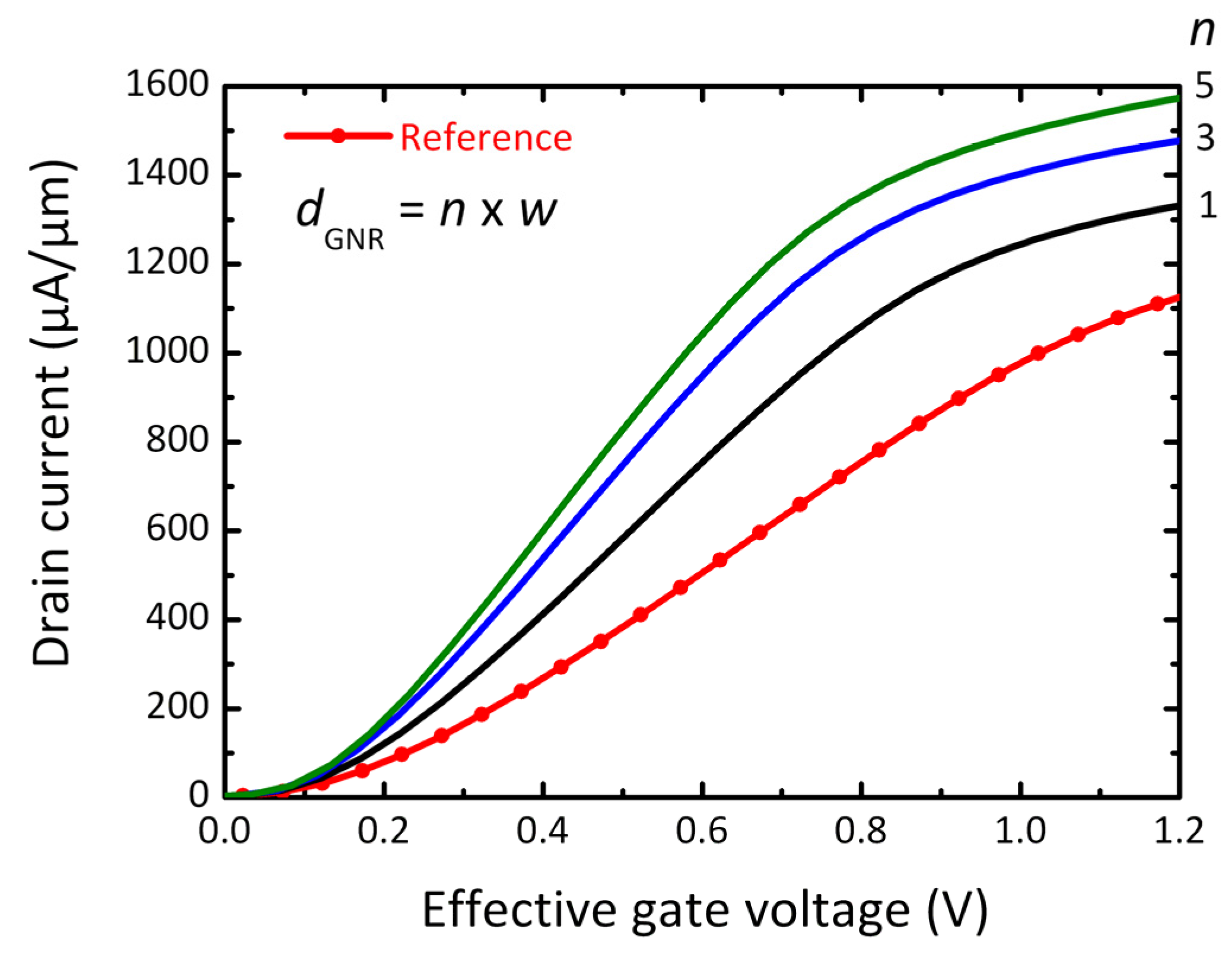
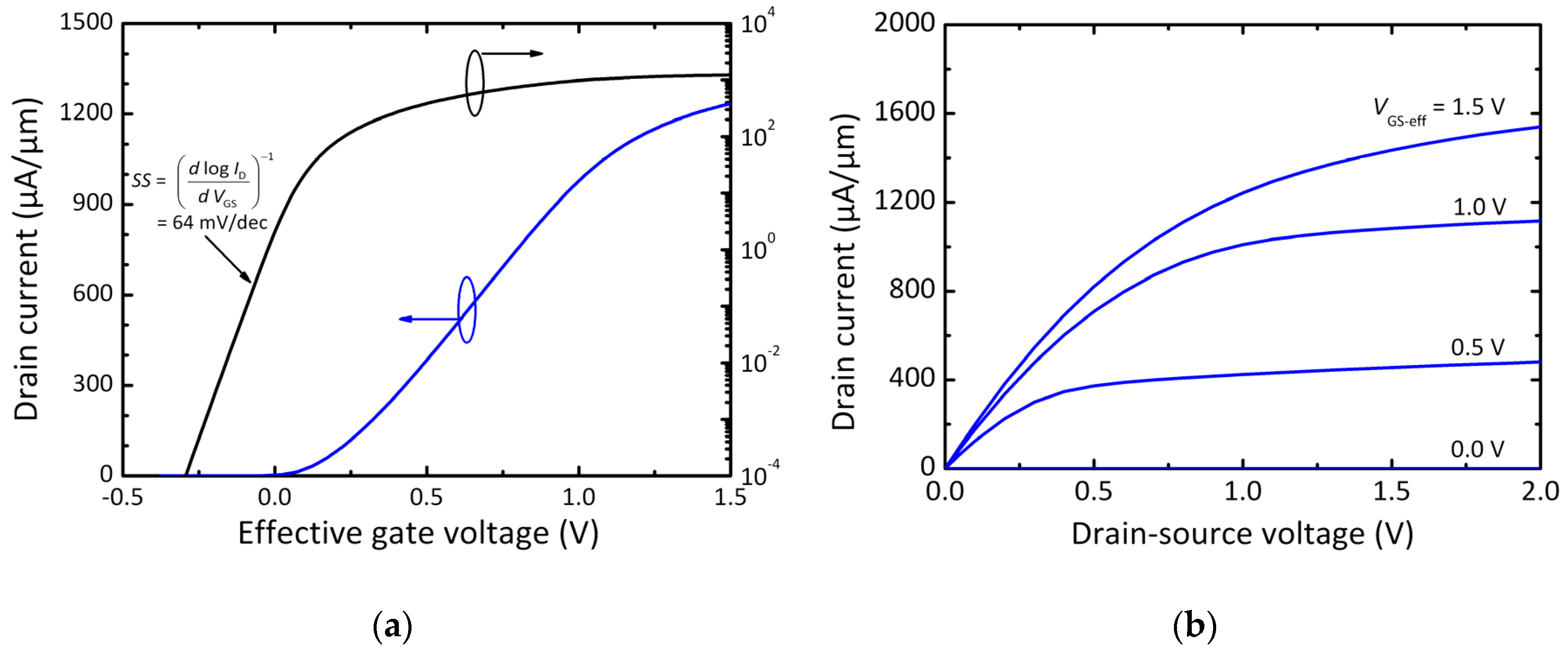
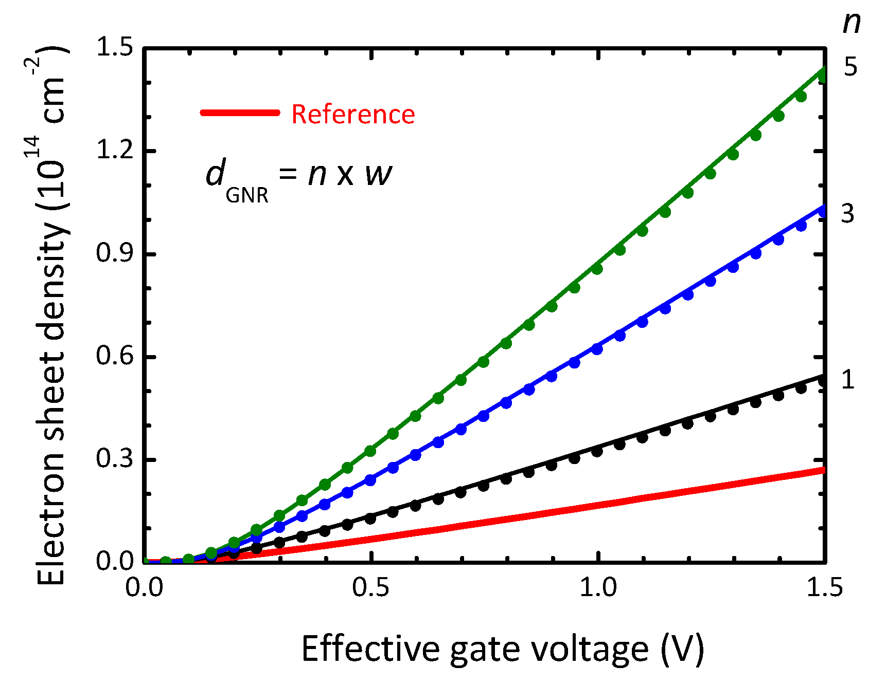
3.2. Simulation Results for Single-Channel GNR MOSFETs

Figure 5a shows the simulated transfer characteristics of the 50-nm gate single-channel N = 7 ac GNR MOSFET for a drain-source voltage VDS of 1 V. We define transistor’s threshold voltage VTh as the gate-source voltage for which at VDS = 1 V a drain current of 10−7 A × w/L flows and the effective gate-source voltage VGS-eff is related to the applied gate-source voltage VGS by VGS-eff = VGSVTh. As to be expected from the 1.4 eV bandgap of the N = 7 GNR channel, the transistors shows excellent switch-off, an on-off ratio of 1.5 × 10⁶ for a 1 V gate voltage swing (from VGS-eff = −0.25 V to +0.75 V), and a nearly ideal subthreshold swing SS of 64 mV/dec. The transconductance (not shown in the Figure) peaks at an effective gate voltage around 0.68 V reaching 1.25 mS/µm.
Figure 5. Steady-state characteristics of the simulated 50-nm gate single-channel GNR MOSFET: (a) transfer characteristics; and (b) output characteristics.
Electronics 05 00003 g005
The output characteristics of the same transistor depicted in Figure 5b shows a pronounced saturation of the drain current and a low drain conductance of 76 µS/µm at VDS = 1 V and VGS-eff = 0.5 V. The good current saturation is caused by the semiconducting nature of the GNR channel and marks, in addition to the high on-off ratio, an important improvement compared to GFETs with gapless large-area graphene channels which suffer from a weak saturation and a large drain conductance.
To get an impression on RF potential of GNR FETs, we also perform small-signal analyses for the 50-nm gate single-channel GNR MOSFET and calculate its small-signal current gain h21 and unilateral power gain U at a frequency of 10 GHz for VDS = 1 V and varying VGS-VTh. The cutoff frequency fT and the maximum frequency of oscillation fmax are then obtained by extrapolating h21 and U with the characteristic slope of −20 dB/dec to zero dB [44]. A peak cutoff frequency of 215 GHz is obtained at VGS-eff around 0.56 V. Figure 6a compares this result with the best experimental fT data reported for competing RF FETs, i.e., GFETs, Si MOSFETs, and III–V HEMTs (high electron mobility transistor) with comparable gate lengths. As can be seen, in terms of fT our GNR MOSFET performs worse compared to best GFETs and the other competing RF FETs. This was to be expected because of the relatively low mobility in the GNR channel, particularly compared to the gapless large-area graphene channels of GFET and the InGaAs channels (with high In content) of the III–V HEMTs.
Figure 6. RF performance of the simulated 50-nm gate single-channel GNR MOSFET and of competing RF FETs (experimental data) with comparable gate length in terms of cutoff frequency fT and maximum frequency of oscillation fmax: (a) cutoff frequency; and (b) maximum frequency of oscillation. The numbers at the data points indicate the gate length of the corresponding transistor in nm (at the left) and the frequency fT or fmax in GHz (at the right). The data for the experimental GFETs, Si MOSFETs, and III–V HEMTs are taken from the compilations in [4,5,6,31,45].
Electronics 05 00003 g006
While a high fT is certainly desirable for a good RF FET, the more important RF figure of merit is the maximum frequency of oscillation fmax. Figure 6b compares experimental fmax data of competing RF FETs with the simulated fmax of our 50-nm gate GNR MOSFETs. Since the gate resistance has a strong impact on fmax, Figure 6b contains two simulated fmax data points for the GNR MOSFET. The higher fmax of 1.04 THz has been simulated assuming the idealized case of zero gate resistance and the second fmax of 413 GHz has been calculated for the more realistic case assuming a gate resistance RG equal to the source access resistance RS of the GNR MOSFET. As can be seen, the experimental GFETs suffer from poor maximum frequencies of oscillation, mainly due to their unsatisfying current saturation and the resulting large drain conductance causing limited power gain [5]. On the other hand, the simulated fmax performance of the GNR MOSFET is better than that of the best Si MOSFETs, even for the case RG = RS, and only the III–V HEMTs perform noticeably better than the GNR MOSFET.

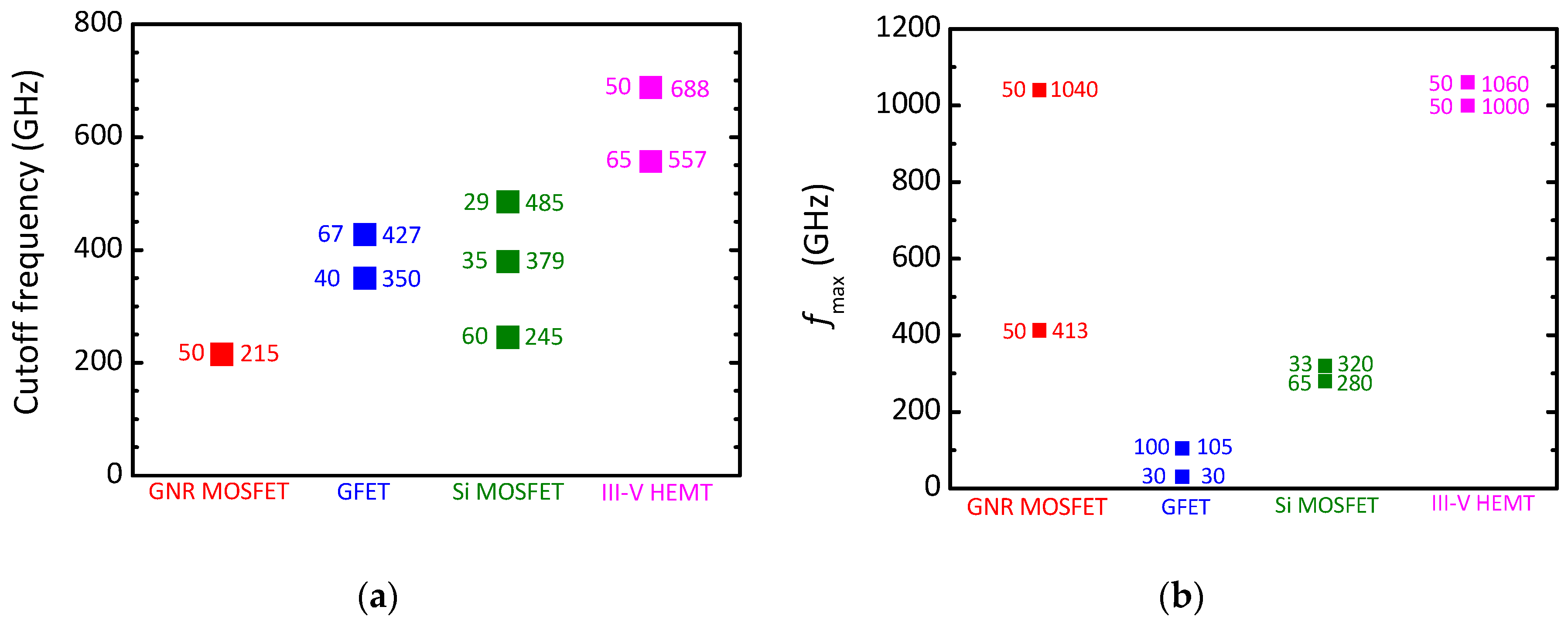
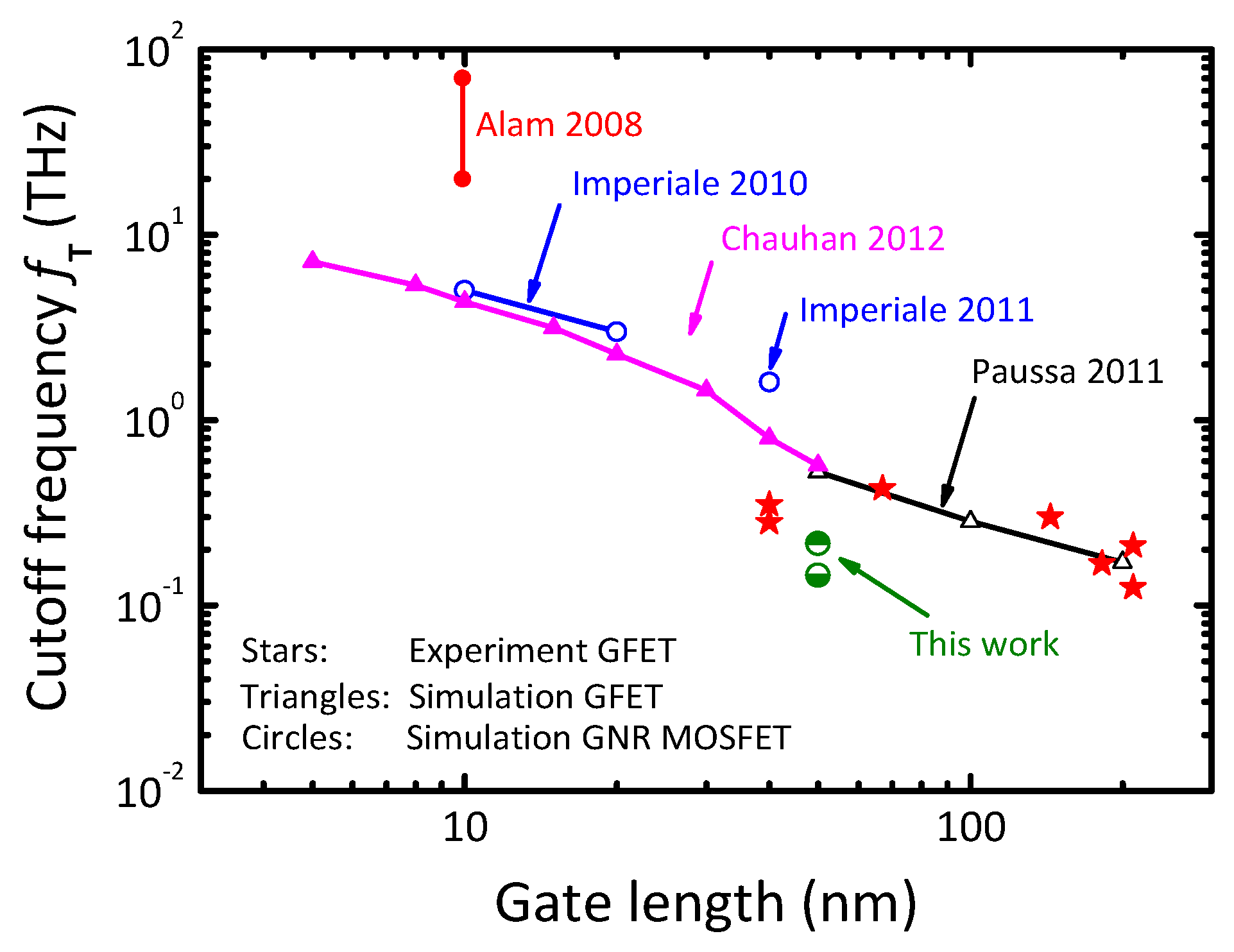
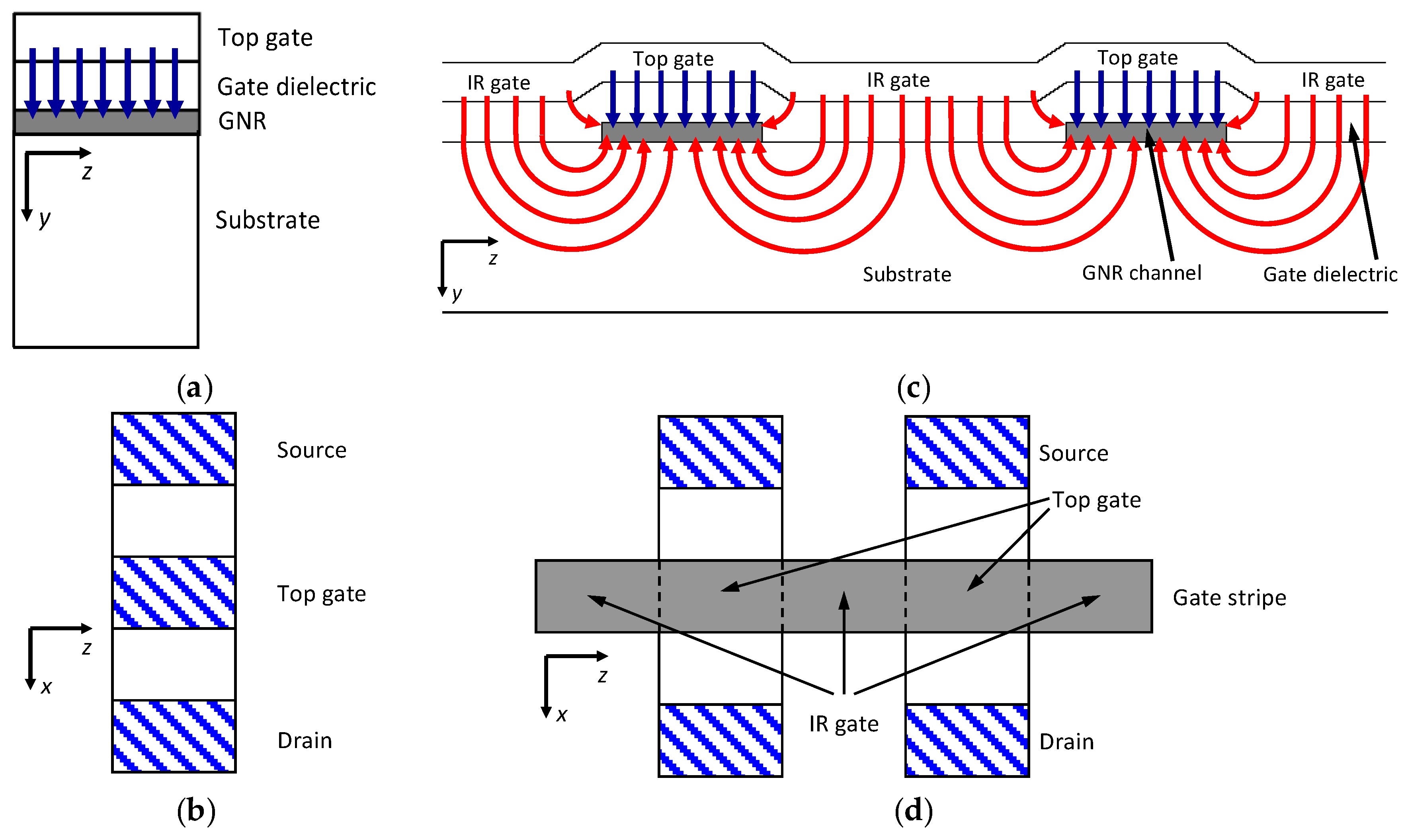
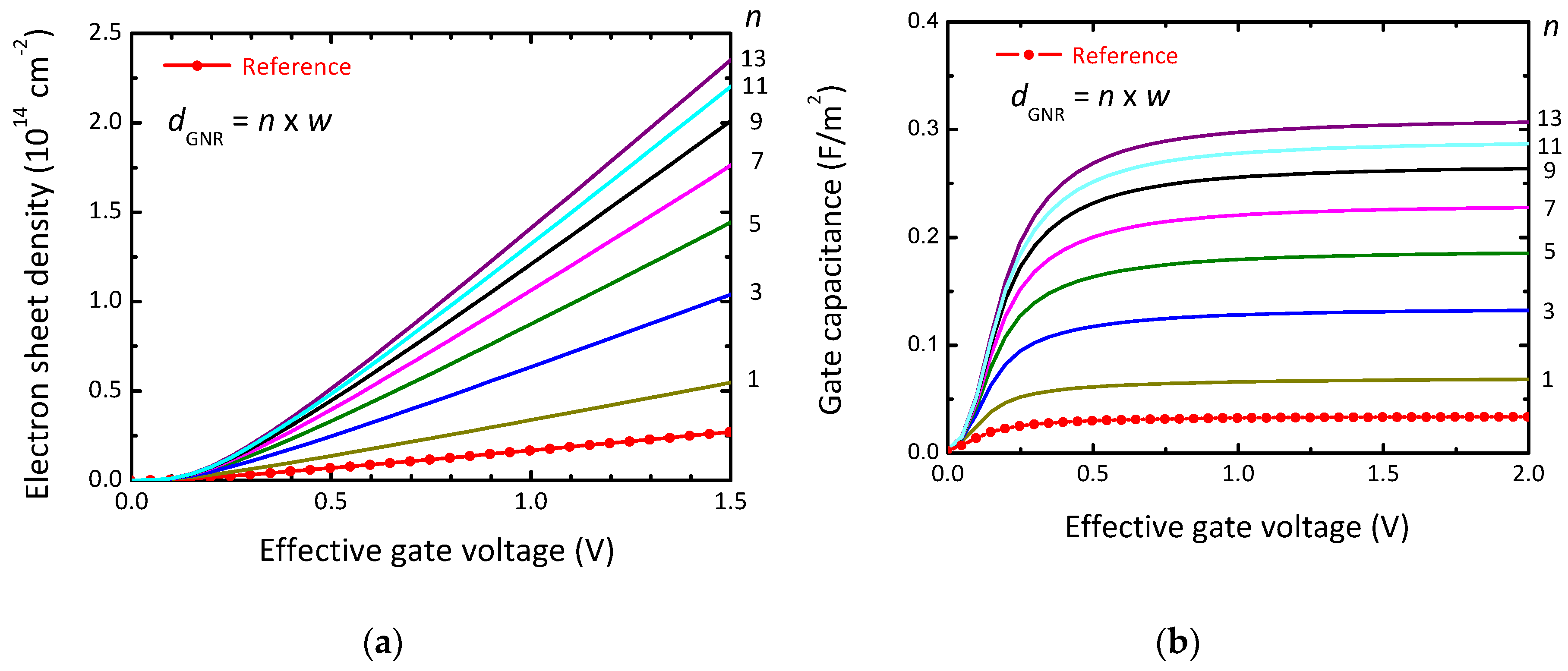
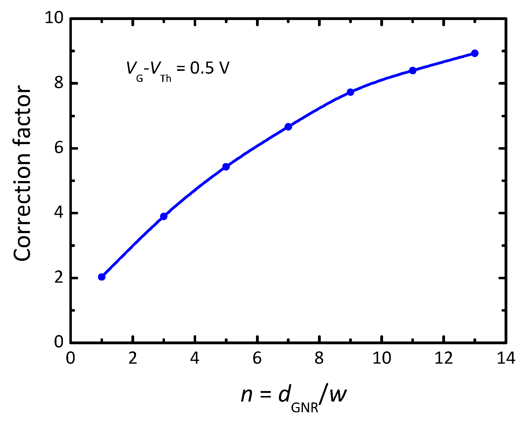
3.3. Simulation Results for Multiple-Channel GNR MOSFETs with Interribbon Gates

To simulate multiple-channel GNR MOSFETs with interribbon gates as shown in Figure 4c,d correctly and to describe the interribbon gate effect accurately, full 3D device simulations would be necessary. It is possible, however, to get a sufficiently good impression on the behavior of multiple-channel GNR MOSFETs by 2D simulations when applying the approach described in the following.
In a first step we perform 2D simulations perpendicular to the direction of current flow, i.e., in the y-z plane, see Figure 4, for zero applied drain-source voltage and calculate the electron sheet density nsh and the gate capacitance CG given by
C G = q d n sh d V GS
This is done twice, first for the simplified structure without interribbon gate shown in Figure 4a and second for structures with interribbon gates, see Figure 4c. Figure 7a shows the calculated electron sheet density as a function of the effective gate voltage for GNR MOS structures (i) with a single GNR channel and top gate only; and (ii) multiple parallel GNR channels, interribbon gates, and varying separations dGNR between adjacent GNRs. Clearly the interribbon gates have a significant effect on the sheet density (nsh is much larger for the structures with interribbon gate compared to the simple structure without interribbon gate) and this effect is getting more pronounced for increasing GNR separation. The corresponding gate capacitance is shown in Figure 7b. A simple way to emulate the effect of the interribbon gates on the channel, even if only the simplified structure from Figure 4a, i.e., without interribbon gate, is simulated, is to modify (increase) the dielectric constants of the gate oxide and of the GNRs by a correction factor. Figure 8 shows the correction factor for the gate capacitance, and thus for the dielectric constants, needed to reproduce the gate capacitance for a multiple-channel structure with interribbon gate.
Figure 7. (a) Electron sheet density and (b) gate capacitance of multiple-channel GNR MOS structures with interribbon gates as a function of the effective gate voltage for different separations dGNR between adjacent GNRs (lines). The sheet density and the gate capacitance obtained for the single-channel GNR MOS structure without interribbon gate are also shown (red lines with symbols, designated as Reference).
Electronics 05 00003 g007
Figure 8. Correction factor for the dielectric constants of the top-gate dielectric and the GNR that reproduces the effect of the interribbon gate. Note that the correction factor has been determined for one single effective gate voltage (0.5 V).
Electronics 05 00003 g008
Figure 9 shows that by applying the correction factor approach, the sheet density of multiple-channel GNR MOS structures with interribbon gates can be perfectly reproduced, even if only a single-channel structure without interribbon-gate is simulated. Note that the perfect agreement for effective gate voltages in the range 0–1.5 V has been obtained by multiplying the original dielectric constants for both the top-gate dielectric (εr = 25) and the GNR (εr = 1.8) by the correction factor from Figure 8, i.e., the correction factor that has been elaborated for one single operating point (VGS-eff = 0.5 V).
Having the correction factor approach established, in a second step we investigate how the interribbon gates affect the drain currents and the RF performance (in terms of fT) of GNR MOSFETs by applying this approach. Figure 10 shows the transfer characteristics of three multiple-channel GNR MOSFETs having different separations between adjacent channels and of a single-channel transistor with top gate only and no interribbon gates. As to be expected from the enhanced carrier sheet density (see Figure 9), the drain currents of the structures with interribbon gates are noticeably larger compared to that of the simplified structure without interribbon gate. Moreover, the slopes of the transfer characteristics for the multiple-channel GNR MOSFETs are larger than that of the single-channel MOSFET, i.e., multiple-channel MOSFETs show a higher transconductance.
Figure 9. Electron sheet density in multiple-channel GNR MOS structures as a function of effective gate voltage. Green, blue, and black lines: Obtained when simulating the multiple-channel GNR MOS structure from Figure 4c, thereby using the original values for the dielectric constants for the gate dielectric (εr = 25) and the GNRs (εr = 1.8). Symbols: Obtained by simulating the single-channel GNR MOS structure from Figure 4a applying the correction factor method. Thick red line: Obtained by simulating the single-channel GNR MOS structure from Figure 4a, thereby using the original values for the dielectric constants for the gate dielectric (εr = 25) and the GNRs (εr = 1.8), designated as Reference.
Electronics 05 00003 g009
Figure 10. Transfer characteristics of multiple-channel GNR MOSFETs applying the correction factor approach (green, blue, and black lines). The transfer characteristics of the single-channel GNR MOSFET without interribbon gate (red line with symbols, designated as Reference), i.e., the characteristics obtained using the original values of the dielectric constants of the gate dielectric (εr = 25) and the GNRs (εr = 1.8) are also shown.
Electronics 05 00003 g010
On the other hand, the interribbon gates deteriorate the RF performance. While, as already shown in Figure 6a, the single-channel GNR MOSFET achieves a peak fT of 215 GHz, the multiple-channel transistors show lower cutoff frequencies of 184 GHz, 158 GHz, and 145 GHz for GNR separations dGNR of 1 × w, 3 × w, and 5 × w (w is the GNR width), respectively. This effect looking surprising on first view is closely related to the observed degradation of the RF performance of Si FinFETs and Si tri-gate MOSFETs compared to their planar counterparts [46]. The degraded cutoff frequencies originate from additional capacitance components caused by the interribbon gates. These contribute to the current control less efficiently than the top gate capacitance leading to the situation that the effect of the increased gate capacitance cannot be fully compensated by the enhanced transconductance, i.e., in multiple-channel GNR MOSFETs with interribbon gates the transconductance increases to a lesser extent than the gate capacitance. We note, however, that the interribbon gates will lead to a better suppression of short-channel effects and improve the scaling behavior of GNR MOSFETs. Such a combination of an improved scaling behavior and simultaneously degraded RF performance is not specific for GNR MOSFETs but has also been observed in Si FinFETs and Si tri-gate MOSFETs since the interribbon gate of multiple-channel GNR MOSFETs resembles the sidewall gates of FinFETs and tri-gate FETs. The maximum frequency of oscillation fmax of multiple-channel GNR MOSFETs will be affected by the additional capacitance of the interribbon gates to a similar extent as the cutoff frequency fT since both fT and fmax are roughly proportional to gm/Cgs where gm is the transconductance and Cgs is the gate-source capacitance (that includes contributions from both the top gate and the interribbon gate), see, e.g., Equations (3) and (4) in [5].
Figure 11 shows how our calculated cutoff frequencies for the single-channel and multiple-channel GNR MOSFETs compare to the cutoff frequencies simulated by other groups for GNR MOSFETs and GFETs and to the best reported cutoff frequencies of experimental GFETs. Experimental GNR MOSFETs could not be included in Figure 11 since the RF performance of such transistors has not been reported so far.
Figure 11. Simulated cutoff frequency of GNR MOSFETs and GFETs as a function of gate length. Data taken from the literature [21,22,47,48] and from the present work. fT data of experimental GFETs and data taken from the compilations in are also shown [5,6]. The two data points designated by this work correspond to the cutoff frequency of the single-channel GNR MOSFETs, see also Figure 6a, and of the multiple-channel GNR MOSFET with a GNR separation of 5 × w.
Electronics 05 00003 g011
As can be seen, our simulated cutoff frequencies for 50-nm gate GNR MOSFETs are lower than those calculated for GFETs with the same gate length by Chauhan et al. [47] and Paussa et al. [48], both taking phonon scattering into account. This is reasonable since carrier transport in GNRs is degraded compared to that in gapless large-area graphene. Comparing our simulated fT data with the calculated cutoff frequencies for GNR MOSFETs from [25], where phonon scattering has been taken into account, and those from [21,22] is more difficult since in [21,22,25] transistors with much shorter gates have been considered. Figure 11 shows, however, that our cutoff frequencies are by trend lower than those simulated in [21,22,25]. Although the approach used in the present work is engineering-style and involves less physics than the simulations from [21,22,25] we believe that our results are reasonable. The GNR channels considered in [22,25] have been assumed to be 10 nm wide and have a gap of 0.14 eV only compared to 1.4 eV in our more narrow GNRs. This means that carrier transport in the 10-nm wide ribbons is less degraded than in our GNRs. The simulations in [21,22], on the other hand, assume ballistic transport and therefore are expected to overestimate transistor performance.

4. Conclusions

An engineering approach to simulate the steady-state and small-signal behavior of GNR MOSFETs based on a classical 2D device simulator is presented. Modifications implemented in a commercial simulator enable taking the 1D DOS and the material properties of GNRs into account and allow the correct reproduction of the quantum capacitance of GNR MOS structures and of the effects of interribbon gates in multiple-channel GNR MOSFETs. Exemplarily, 50-nm gate ac N = 7 GNR MOSFETs in both single-channel and multiple-channel configurations have been investigated in detail. It is shown that multiple-channel GNR transistors show higher normalized drain currents and transconductances compared to their single-channel counterparts. On the other hand, the interribbon gates cause additional gate capacitance components whose effects cannot fully be compensated by the enhanced transconductance. Moreover, GNR MOSFETs show lower cutoff frequencies than GFETs due to the degraded mobility in narrow GNRs. At the same time, however, the maximum frequency of oscillation of GNR MOSFETs is significantly higher compared to that of GFET due to the semiconducting nature of the GNR channel.

Acknowledgments

This work has been supported by Excellence Research and Intra-Faculty Research Grants of Technische Universität Ilmenau, Germany, and by DFG under contract numbers SCHW 729/16-1 and PE 624/11-1.

Author Contributions

Cedric Nanmeni Bondja developed the approach to account for the 1D density of states in ATLAS, developed the transport model, and performed the simulations; Zhansong Geng performed simulations; Ralf Granzner defined the simulated device structures and analyzed the simulation results; Jörg Pezoldt contributed to the definition of the simulated device structures and to the interpretation of the results; Frank Schwierz conceived the simulation study, compared the simulation results with experimental data and simulation results from the literature, and wrote the paper.

Conflicts of Interest

The authors declare no conflict of interest.

Appendix

In the following, the expressions for the calculation of the carrier sheet density (in units of cm−2) and the quantum capacitance for the 3D (bulk) case [42], the 2D case, and the 1D case [42], which have been used in Section 2.3, are summarized.
3D case
n sh 3 D = t c 0 g 3 D ( ε ) f ( ε q φ c ) d ε
g 3 D ( ε ) = ν m eff 2 m eff ε π 2 3
f ( ε q φ c ) = 1 1 + exp ( ε q φ c k B T )
C q 3 D = ν q 2 t c m eff 2 m eff 4 k B T π 2 3 0 ε cosh 2 ( ε q φ c 2 k B T ) d ε
2D case
n sh 2 D = i 0 g 2 D i f ( ε , E i ) d ε
g 2 D i = ν i m effi π 2
f ( ε , E i ) = 1 1 + exp ( ε + E i q φ c k B T )
C q 2 D = q 2 π 2 i ν i m effi 1 + exp ( E i q φ c k B T )
1D case
n sh 1 D = 1 w i 0 g 1 D i f ( ε , E i ) d ε
g 1 D i ( ε ) = ν i π 2 m effi ε
C q 1 D = q 2 w 2 h k B T i ν i m effi 0 1 ε cosh 2 ( ε + E i q φ s 2 k B T ) d ε
where φc is the channel potential given by −(ECEF)/q, q is the elementary charge, ε is the kinetic energy of the electrons, g is the density of states (gi is the density of states in the ith subband), tc is the GNR thickness, ν is the valley degeneracy factor, meff is the density of states effective mass, f is the Fermi–Dirac distribution function, Ei is the position of the ith subband with respect to the conduction band edge, kB is the Boltzmann constant, and T is the temperature. Note that the expression for the quantum capacitance for the 2D case, i.e., Equation (A8), does not contain an integral since for the expression of the sheet density, i.e., Equation (A5), an analytical solution can be derived.
In the ATLAS simulations, the basic semiconductor equations, i.e., Poisson’s equation, the current equations for electrons and holes (using Equation (4) with the parameters given below Table 1), and the continuity equations, are solved self-consistently.

References

  1. Geim, A.K.; Novoselov, K.S. The rise of graphene. Nat. Mater. 2007, 6, 183–191. [Google Scholar] [CrossRef] [PubMed]
  2. Wu, Y.; Jenkins, K.A.; Valdes-Garcia, A.; Farmer, D.B.; Zhu, Y.; Bol, A.A.; Dimitrakopoulos, C.; Zhu, W.; Xia, F.; Avouris, P.; et al. State-of-the-art graphene high-frequency electronics. Nano Lett. 2012, 2, 3062–3067. [Google Scholar] [CrossRef] [PubMed]
  3. Cheng, R.; Bai, J.; Liao, L.; Zhou, H.; Chen, Y.; Liu, L.; Lin, Y.-C.; Jiang, S.; Huang, Y.; Duan, X. High-frequency self-aligned graphene transistors with transferred gate stacks. Proc. Natl. Acad. Sci. USA 2012, 109, 11588–11592. [Google Scholar] [CrossRef] [PubMed]
  4. Schwierz, F. Graphene transistors. Nat. Nanotechnol. 2010, 5, 487–496. [Google Scholar] [CrossRef] [PubMed]
  5. Schwierz, F. Graphene transistors: Status, prospects, and problems. Proc. IEEE 2013, 101, 1567–1584. [Google Scholar] [CrossRef]
  6. Lemme, M.C.; Li, L.-J.; Palacios, T.; Schwierz, F. Two-dimensional materials for electronic applications. MRS Bull. 2014, 39, 711–718. [Google Scholar] [CrossRef]
  7. Castro, E.V.; Novoselov, K.S.; Morozov, S.V.; Peres, N.M.R.; Lopes-dos-Santos, J.M.B.; Nilsson, J.; Guinea, F.; Geim, A.K.; Castro-Neto, A.H. Biased bilayer graphene: Semiconductor with a gap tunable by the electric field effect. Phys. Rev. Lett. 2007, 99, 216802. [Google Scholar] [CrossRef] [PubMed]
  8. Szafranek, B.N.; Fiori, G.; Schall, D.; Neumaier, D.; Kurz, H. Current saturation and voltage gain in bilayer graphene field effect transistors. Nano Lett. 2012, 12, 1324–1328. [Google Scholar] [CrossRef] [PubMed]
  9. Han, M.Y.; Özyilmaz, B.; Zhang, Y.; Kim, P. Energy band-gap engineering of graphene nanoribbons. Phys. Rev. Lett. 2007, 98, 206805. [Google Scholar] [CrossRef] [PubMed]
  10. Linden, S.; Zhong, D.; Timmer, A.; Aghdassi, N.; Franke, J.H.; Zhang, H.; Feng, X.; Müllen, K.; Fuchs, H.; Chi, L.; et al. Electronic structure of spatially aligned graphene nanoribbons on Au(788). Phys. Rev. Lett. 2012, 108, 216801. [Google Scholar] [CrossRef] [PubMed]
  11. Liang, X.; Jung, Y.-S.; Wu, S.; Ismach, A.; Olynick, D.L.; Cabrini, S.; Bokor, J. Formation of bandgap and subbands in graphene nanomeshes with sub-10 nm ribbon width fabricated via nanoimprint lithography. Nano Lett. 2010, 10, 2454–2460. [Google Scholar] [CrossRef] [PubMed]
  12. Berrada, S.; Nguyen, V.H.; Querlioz, D.; Saint-Martin, J.; Alarcon, A.; Chassat, C.; Bournel, A.; Dollfus, P. Graphene nanomesh transistor with high on/off ratio and good saturation behavior. Appl. Phys. Lett. 2013, 103, 183509. [Google Scholar] [CrossRef]
  13. Raza, H.; Kan, E.C. Armchair graphene nanoribbons: Electronic structure and electric-field modulation. Phys. Rev. B 2008, 77, 245434. [Google Scholar] [CrossRef]
  14. Yang, L.; Park, C.-H.; Son, Y.-W.; Cohen, M.L.; Louie, S.G. Quasiparticle energies and band gaps in graphene nanoribbons. Phys. Rev. Lett. 2007, 99, 186801. [Google Scholar] [CrossRef] [PubMed]
  15. Gunlycke, D.; White, C.T. Tight-binding energy dispersions of armchair-edge graphene nanostripes. Phys. Rev. B 2008, 77, 115116. [Google Scholar] [CrossRef]
  16. The International Technology Roadmap for Semiconductors. Available online: http://www.itrs.net (accessed on 15 October 2015).
  17. Li, X.; Wang, X.; Zhang, L.; Lee, S.; Dai, H. Chemically derived, ultrasmooth graphene nanoribbon semiconductors. Science 2008, 319, 1229–1232. [Google Scholar] [CrossRef] [PubMed]
  18. Wang, X.; Ouyang, Y.; Li, X.; Wang, H.; Guo, J.; Dai, H. Room-temperature all-semiconducting sub-10-nm graphene nanoribbon field-effect transistors. Phys. Rev. Lett. 2008, 100, 206803. [Google Scholar] [CrossRef] [PubMed]
  19. Bai, J.; Duan, X.; Huang, Y. Rational fabrication of graphene nanoribbons using a nanowire etch mask. Nano Lett. 2009, 9, 2083–2087. [Google Scholar] [CrossRef] [PubMed]
  20. Liao, L.; Bai, J.; Cheng, R.; Lin, Y.-C.; Jiang, S.; Huang, Y.; Duan, X. Top-gated graphene nanoribbon transistors with ultrathin high-k dielectrics. Nano Lett. 2010, 10, 1917–1921. [Google Scholar] [CrossRef] [PubMed]
  21. Alam, K. Gate dielectric scaling of top gate carbon nanoribbon on insulator transistors. J. Appl. Phys. 2008, 104, 074313. [Google Scholar] [CrossRef]
  22. Imperiale, I.; Gnudi, A.; Gnani, E.; Reggiani, S.; Baccarani, G. High-frequency analog GNR-FET design criteria. In Proceedings of the 2011 European Solid-State Device Research Conference (ESSDERC), Helsinki, Finland, 12–16 September 2011; pp. 303–306.
  23. Harada, N.; Sato, S.; Yokoyama, N. Theoretical investigation of graphene nanoribbon field-effect transistors designed for digital applications. Jpn. J. Appl. Phys. 2013, 52, 094301. [Google Scholar] [CrossRef]
  24. Liang, G.; Neophytou, N.; Lundstrom, M.S.; Nikonov, D.E. Ballistic graphene nanoribbon metal-oxide-semiconductor field-effect transistors: A full real-space quantum transport simulation. J. Appl. Phys. 2007, 102, 054307. [Google Scholar] [CrossRef]
  25. Imperiale, I.; Bonsignore, S.; Gnudi, A.; Gnani, E.; Reggiani, S.; Baccarani, G. Computational study of graphene nanoribbon FETs for RF applications. In Proceedings of the 2010 IEEE International Electron Devices Meeting (IEDM), San Francisco, CA, USA, 6–8 December 2010; pp. 732–735.
  26. Fiori, G.; Iannaccone, G. Simulation of graphene nanoribbon field-effect transistors. IEEE Electron Device Lett. 2007, 8, 760–762. [Google Scholar] [CrossRef]
  27. Goharrizi, A.Y.; Pourfarth, M.; Fathipour, M.; Kosina, H. Device performance of graphene nanoribbon field-effect transistors in the presence of edge-line roughness. IEEE Trans. Electron Devices 2012, 59, 3527–3532. [Google Scholar] [CrossRef]
  28. Kliros, G.S. Gate capacitance modeling and width-dependent performance of graphene nanoribbon transistors. Microelctron. Eng. 2013, 112, 220–226. [Google Scholar] [CrossRef]
  29. Bruzzone, S.; Iannaccone, G.; Marzari, N.; Fiori, G. An open-source multiscale framework for the simulation of nanoscale devices. IEEE Trans. Electron Devices 2014, 61, 48–53. [Google Scholar] [CrossRef]
  30. ATLAS User’s Manual—Device Simulation Software, Silvaco. Available online: http://dynamic.silvaco.com/dynamicweb/jsp/downloads/DownloadManualsAction.do?req=silentmanuals&nm=atlas (accessed on 15 October 2015).
  31. Schwierz, F.; Pezoldt, J.; Granzner, R. Two-dimensional materials and their prospects in transistor applications. Nanoscale 2015, 7, 8261–8283. [Google Scholar] [CrossRef] [PubMed]
  32. Ruffieux, P.; Cai, J.; Plumb, N.; Patthey, L.; Prezzi, D.; Ferretti, A.; Molinari, E.; Feng, X.; Müllen, K.; Pignedoli, C.A.; et al. Electronic structure of atomically precise graphene nanoribbons. ACS Nano 2012, 6, 6930–6935. [Google Scholar] [CrossRef] [PubMed]
  33. Chen, Y.-C.; de Oteyza, D.G.; Pedramrazi, Z.; Chen, C.; Fischer, F.R.; Crommie, M.F. Tuning the band gap of graphene nanoribbons synthesized from molecular precursors. ACS Nano 2013, 7, 6123–6128. [Google Scholar] [CrossRef] [PubMed]
  34. Fang, T.; Konar, A.; Xing, H.; Jena, D. Carrier statistics and quantum capacitance of graphene sheets and ribbons. Appl. Phys. Lett. 2007, 91, 092109. [Google Scholar] [CrossRef]
  35. Granzner, R.; Polyakov, V.M.; Schwierz, F.; Kittler, M.; Luyken, R.J.; Rösner, W.; Städele, M. Simulation of nanoscale MOSFETs using modified drift-diffusion and hydrodynamic models and comparison with Monte Carlo results. Microelectron. Eng. 2006, 83, 241–246. [Google Scholar] [CrossRef]
  36. Szabo, A.; Rhyner, R.; Luisier, M. Ab-initio simulations of MoS2 transistors: From mobility calculation to device performance evaluation. In Proceedings of the 2014 IEEE International Electron Devices Meeting (IEDM), San Francisco, CA, USA, 15–17 December 2014; pp. 725–728.
  37. Cao, W.; Kang, J.; Sarkar, D.; Liu, W.; Banerjee, K. Performance evaluation and design considerations of 2D semiconductor based FETs for sub-10 nm VLS. In Proceedings of the 2014 IEEE International Electron Devices Meeting (IEDM), San Francisco, CA, USA, 15–17 December 2014; pp. 729–732.
  38. Liu, L.; Lu, Y.; Guo, J. On monolayer MoS2 field-effect transistors at the scaling limit. IEEE Trans. Electron Devices 2013, 60, 4133–4139. [Google Scholar] [CrossRef]
  39. Ancona, M.G. Electron transport in graphene from a diffusion-drift perspective. IEEE Trans. Electron Devices 2010, 57, 681–689. [Google Scholar] [CrossRef]
  40. Betti, A.; Fiori, G.; Iannaccone, G. Drift velocity peak and negative differential mobility in high field transport in graphene nanoribbons explained by numerical simulations. Appl. Phys. Lett. 2011, 99, 242108. [Google Scholar] [CrossRef]
  41. Caughey, D.M.; Thomas, R.E. Carrier mobilities in silicon empirically related to doping and field. Proc. IEEE 1967, 52, 2192–2193. [Google Scholar] [CrossRef]
  42. Granzner, R.; Thiele, S.; Schippel, C.; Schwierz, F. Quantum effects on the gate capacitance of trigate SOI MOSFETs. IEEE Trans. Electron Devices 2010, 57, 3231–3237. [Google Scholar] [CrossRef]
  43. Unluer, D.; Tseng, F.; Ghosh, A.W.; Stan, M.R. Monolithically patterned wide-narrow-wide all-graphene devices. IEEE Trans. Nanotechnol. 2011, 10, 931–939. [Google Scholar] [CrossRef]
  44. Schwierz, F.; Liou, J.J. Modern Microwave Transistors; John Wiley & Sons: Hoboken, NJ, USA, 2003. [Google Scholar]
  45. Schwierz, F. Microwave Transistors: State of the Art in the 1980s, 1990s, 2000s, and 2010s. A Compilation of 1500 Top References; TU Ilmenau: Ilmenau, Germany, 2015; unpublished. [Google Scholar]
  46. Kranti, A.; Raskin, J.-P.; Armstrong, G.A. Optimizing FinFET geometry and parasitics for RF applications. In Proceedings of the IEEE International SOI Conference, New Paltz, NY, USA, 6–9 October 2008; pp. 123–124.
  47. Chauhan, J.; Liu, L.; Lu, Y.; Guo, J. A computational study of high-frequency behavior of graphene field-effect transistors. J. Appl. Phys. 2012, 111, 094313. [Google Scholar] [CrossRef]
  48. Paussa, A.; Geromel, M.; Palestri, P.; Bresciani, M.; Esseni, D.; Selmi, L. Simulation of graphene nanoscale RF transistors including scattering and generation/recombination mechanisms. In Proceedings of the 2011 International Electron Devices Meeting, Washington, DC, USA, 5–7 December 2011; pp. 271–274.

