Review

Towards the Realization of Graphene Based Flexible Radio Frequency Receiver

Microelectronics Research Center, Department of Electrical and Computer Engineering, The University of Texas at Austin, Austin, TX 78758, USA
*
Author to whom correspondence should be addressed.
Electronics 2015, 4(4), 933-946; https://doi.org/10.3390/electronics4040933
Submission received: 27 September 2015 / Revised: 30 October 2015 / Accepted: 2 November 2015 / Published: 11 November 2015
(This article belongs to the Special Issue Two-Dimensional Electronics - Prospects and Challenges)

Abstract

:
We report on our progress and development of high speed flexible graphene field effect transistors (GFETs) with high electron and hole mobilities (~3000 cm2/V·s), and intrinsic transit frequency in the microwave GHz regime. We also describe the design and fabrication of flexible graphene based radio frequency system. This RF communication system consists of graphite patch antenna at 2.4 GHz, graphene based frequency translation block (frequency doubler and AM demodulator) and graphene speaker. The communication blocks are utilized to demonstrate graphene based amplitude modulated (AM) radio receiver operating at 2.4 GHz.

1. Introduction

Research efforts in the field of flexible GHz nanoelectronics have been gaining significant momentum recently. Research and commercial institutions are investing substantial resources in the design of flexible systems and sensors [1,2,3,4,5,6,7], including the development of smart conformal devices and tags, wearable electronics, internet of things (IoTS) and other electronic gadgets that are low cost, scalable to large areas, and mechanically robust, which is beyond the capability of conventional bulk semiconductor technologies. Moreover continuous advancements in the material synthesis of intrinsically flexible nanomaterials such as graphene, h-BN, carbon nano-tubes (CNTs) and transition metal dichalcogenides (TMDs, e.g., molybdenum disulfide—MoS2) [8,9] have encouraged their prospects for practical electronic application. These materials are naturally more suitable for integration with flexible, soft or glass substrates owing to their two dimensional nature and can potentially offer the electronic performance needed for low-power GHz systems.
Graphene is a single sheet of carbon with very high room temperature mobility (>10,000 cm2/V·s), high cutoff frequency (>300 GHz), and high electrical and thermal conductivity [2,3,10]. These properties of graphene make it a suitable candidate for the design of high frequency analog communication circuits, such as amplifiers, mixers, demodulators, and speakers [11]. Recent work on graphene circuits for RF applications includes: demonstration of graphene three stage integrated amplifier on Si wafer [12] and demonstration of flexible graphene circuit for a variety of digital modulation schemes [13].
In this paper we present the state of the art flexible graphene field effect transistors (GFET) with high intrinsic fT of 18 GHz that has recently been improved to 100 GHz [14]. We also present the design and realization of the first all graphene based flexible radio frequency system. The following section discusses the design and fabrication of GFETs. Results and discussion section discuss in more detail the small signal modeling, electrical measurements (DC and RF), and mechanical flexibility and reliability evaluation of GFETs. We also discuss the design of individual graphene based radio frequency system blocks—flexible graphite patch antenna, graphene based frequency translation block (GFET doubler and demodulator), graphene speaker, and the demonstration of the first graphene based AM radio receiver.

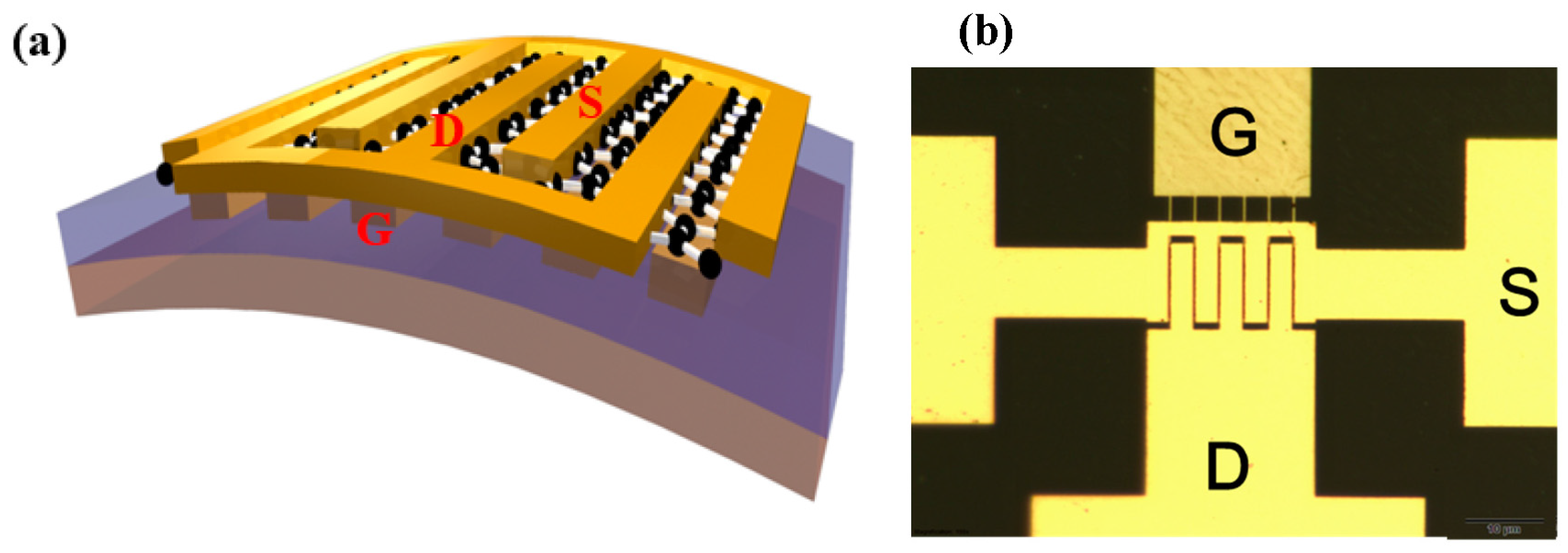
2. Flexible Graphene RF Transistor Fabrication

Figure 1 shows the typical device structure of our fabricated flexible graphene field-effect transistors. GFETs are typically prepared on smoothened commercial 125 µm-thick polyimide (Kapton) films. Gate fingers (evaporated 2 nm Ti/40 nm Pd) and gate dielectric films (prepared by atomic layer deposition of 10 nm-thick Al2O3 or hexagonal boron nitride films) are prepared by electron-beam lithography using JEOL-6000 FSE (JEOL USA Inc., Peabody, MA, 01960, USA). Chemical vapor deposited high-quality graphene films grown on commercial Cu-foils or films are transferred via the conventional wet-transfer process using ammonia persulfate as the Cu-etchant [10]. Active channel area of graphene and metallic electrodes for source and drain contacts are subsequently patterned via additional electron-beam lithography processes. Low power oxygen plasma is used to etch redundant graphene areas and electron-beam evaporation of 2 nm Ti/50 nm Au is used as the contact metals. Figure 1a is 3D view of freestanding polyimide film with multifingered GFET. Figure 1b is the enlarged optical image of a representative GFET fabricated on polyimide substrate. Devices with channel length of 0.25 µm and an effective width of 60 µm (six fingers with 10 µm width) are prepared for electrical measurements, which can afford GHz high frequency performance.
Figure 1. (a) 3D view of multi-fingered GFET on flexible polyimide film; (b) Enlarged optical image of a representative GFET transistor.
Electronics 04 00933 g001

3. Results and Discussion

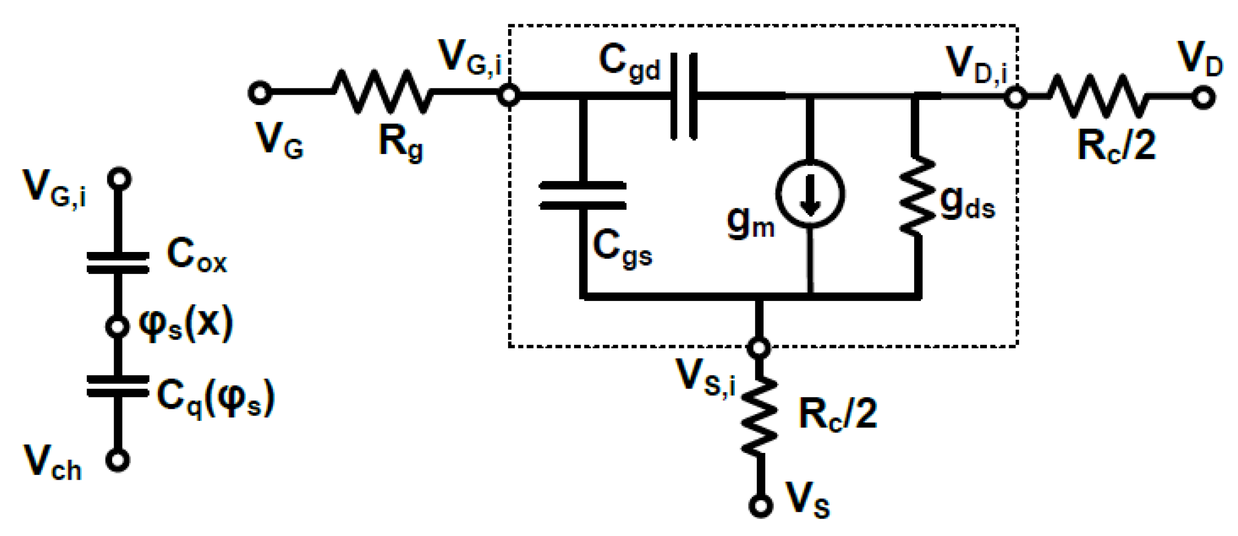
3.1. Compact Model of GFET

We derived a semi-empirical compact model useful for GFET design and analysis. This model shown in Figure 2 has good agreement with DC and RF measurements [15]. In this model we have taken into account the quantum capacitance (Cq), velocity saturation (vsat), contact resistance (Rc) and access resistance (Ra). The derived drain current IDS (see Equation (1)) depends on the graphene channel width (W) and length (L), carrier density (ni), effective mobility(ueff), drain voltage (VDS), gate voltage (VGS), oxide capacitance (COX), quantum capacitance (Cq) and temperature (T). This model is described in more detail in our earlier work [15,16]. This model is implemented in Agilent ADS for linear and nonlinear RF circuit simulation.
Figure 2. Compact model of GFET (adapted from [17]. Copyright 2013, permission granted by Kristen Parish).
Electronics 04 00933 g002
I D S =   q W L μ e f f ( n i V D S + ( ( α + 1 ) 2 ( k B T ln 4 ) 2 4 π ħ 2 v f 2 ( α ln 2 + 1 ) ( 2 V D S + V D G 1 + δ 2 V D G 2 + V G S 1 + δ 2 V G S 2 + asinh δ V D G + asinh δ V G S δ ) )   )
where μ e f f = μ ( 1 + ( μ V D S L v s a t ) 2 ) ; β = q 2 π ħ 2 v f 2 ;   δ = 2 α ( α ln 2 + 1 ) ( α + 1 ) 2 q k B T ln 4 .

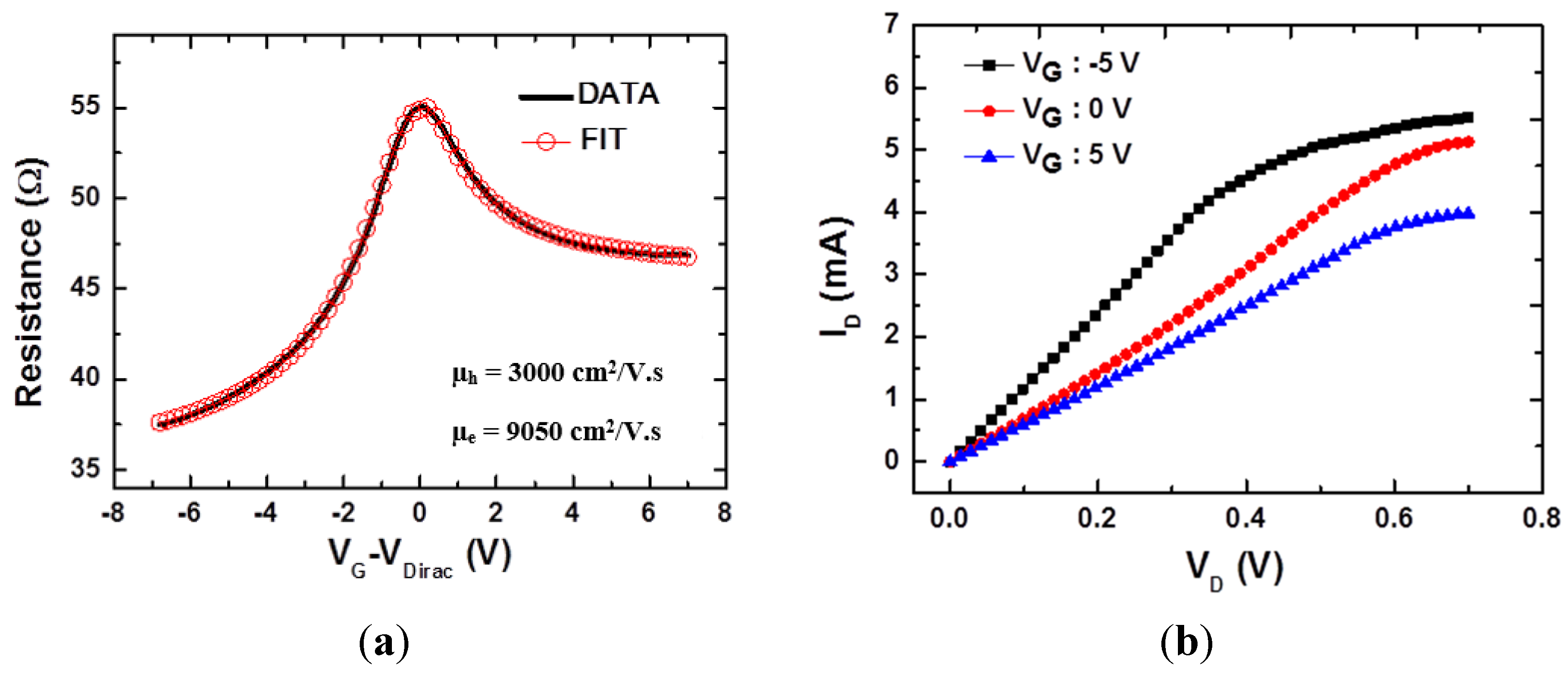
3.2. GFET DC Measurement

Electrical measurements of fabricated GFET are routinely done at room temperature. Figure 3 shows the input and output characteristics of a flexible GFET comparing both model and measured data. The extracted carrier mobility of electrons is 9050 cm2/V·s and that of holes is 3000 cm2/V·s. Graphene FETs show velocity saturation. We attribute this to the smooth surface (surface roughness <1 nm) on polyimide substrate (with liquid polyimide curing) and high K gate dielectric (Al2O3) which will give rise to well-behaved linear current profile followed by saturation [16].
Figure 3. Electrical properties of graphene transistor (a) Gate modulation of graphene resistance. The drain voltage is set to 10 mV; (b) Drain current (ID) vs. Drain voltage (VD).
Electronics 04 00933 g003

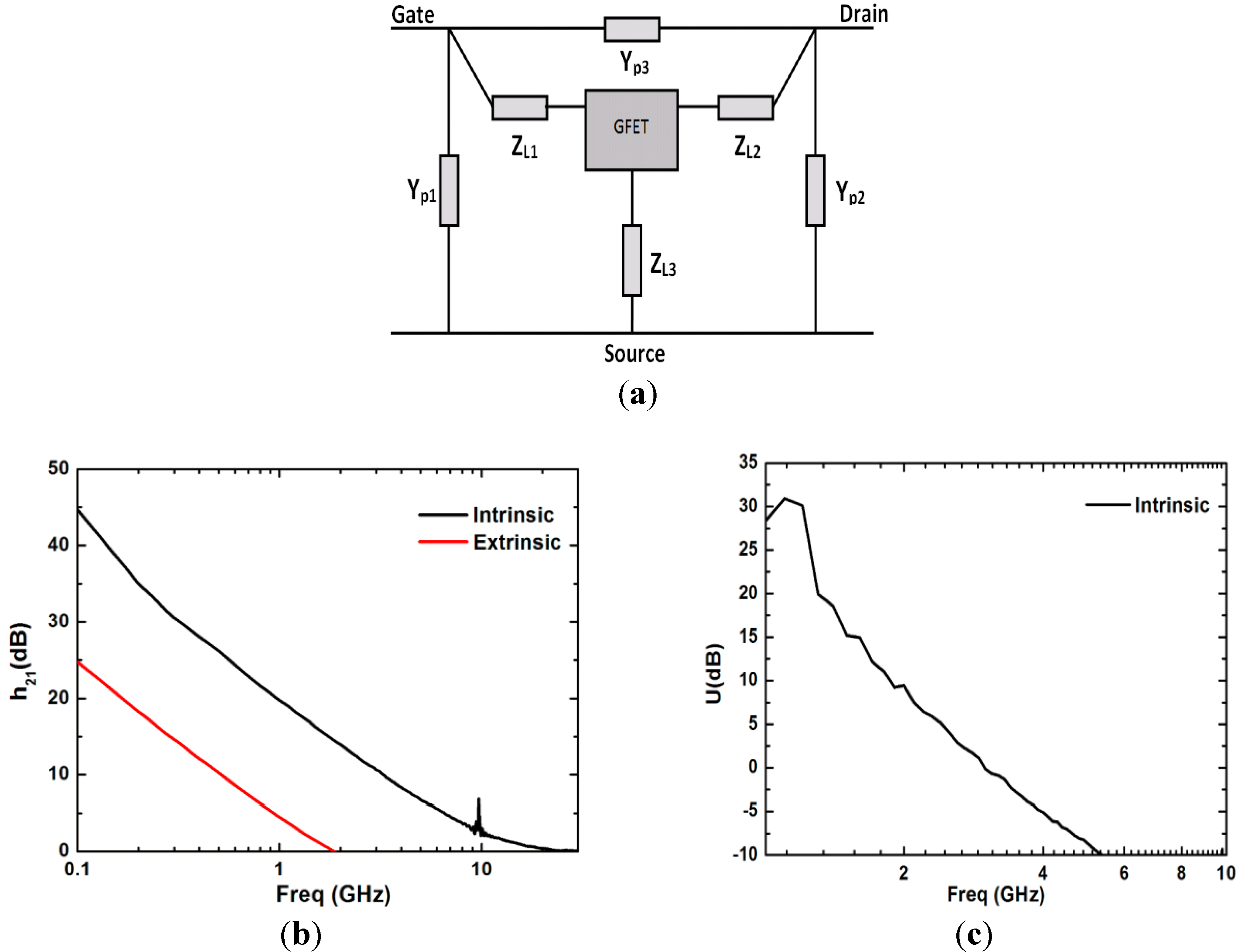
3.3. GFET RF Measurement

S-parameter measurements were carried out on another flexible GFET device with ground-signal-ground (GSG) pads at the gate and drain terminals with the source serving as the common ground. The measurement was done using an Agilent VNA (E8361C) and cascade RF probe station. The intrinsic device data is obtained by employing a two-step de-embedding process. The device under test (GFET) can be modeled as shown in Figure 4a. The Y-parameters of the device under test were obtained from extrinsic data, and afterwards the parasitics (obtained from open and short test structures) were de-embedded to determine the intrinsic device frequency response (see Equation (2), adapted from [18]). The open structure will help to determine parallel parasitics (Yp1, Yp2, Yp3) and the short structure will help to determine the series parasitics (Zl1, Zl2 and Zl3). These series parasitics are very critical for modern small channel FETs.
Y G F E T = ( ( Y d u t Y o p e n ) 1 ( Y s h o r t Y o p e n ) 1 ) 1
where YGFET is the Y-parameters of the intrinsic GFET, Ydut is the Y-parameter of DUT (Extrinsic GFET), Yshort is the Y-parameter of the DUT with gate, drain and source shorted, Yopen is the DUT with no graphene channel. Here, the graphene channel is etched by using reactive ion plasma etch tool. Yshort and Yopen are deembeded from Ydut to obtain the intrinsic GFET performance (YGFET).
Figure 4b shows the current gain h21 of the intrinsic GFET, from which the 18 GHz fT is extracted. The extrinsic fT of the GFET is 1.8 GHz. Figure 4c shows the power gain U (dB) of the intrinsic GFET. We obtained fmax of ~3 GHz. fT and fmax are given by Equations (3) and (4). They depend upon the transconductance gm, gate capacitance Cgs, parasitic gate-drain capacitance Cp,gs, parasitic gate-source capacitance Cp-gd and gate resistance Rg. fT can be improved by reducing channel length and design of better layouts (reduced parasitics) [19]. fT and fmax are lower for flexible devices compared to devices fabricated on rigid substrates mainly due to poor thermal dissipation of flexible polymer substrate at high fields [19]. Thermo-mechanical breakdown occurs when the local hot spot temperature exceeds the glass transition temperature of the soft substrate [2]. One solution to overcome this challenge is to employ flexible glass substrates, such as Corning “willow” glass, which offers a higher thermal conductivity than polymers or elastomers. Indeed, improved high-frequency graphene transistors have been achieved on bendable willow glass with intrinsic fT ~100 GHz and record saturation velocity for flexible graphene [14].
f T = g m 2 π ( C g s + C p , g s + C p , g d ) ( ( R p , s + R p , d ) g d + 1 ) + C p , g d g m ( R p , s + R p , d )
f m a x = f T 2 g d ( R p , s + R g a t e ) + 2 π f T C p , g d R g a t e
Figure 4. (a) RF model of GFET under test, where Yp1, Yp2 and Yp3 are parallel parasitics and ZL1, ZL2 and ZL3 are series parasitics (They represent GFET contact pads and interconnects). (b) Current Gain (h21) vs. Frequency. The intrinsic fT ~18 GHz; (c) Power gain (U) in dB vs. Frequency. fmax ~3 GHz. These devices are measured at the following voltage conditions (Vdrain ~0.4 V, Vgate ~0.2 V).
Electronics 04 00933 g004

3.4. GFET Flexibility and Reliability

Mechanical flexibility of GFET is typically evaluated using custom-made manual bending test fixtures. DC probes were landed on source, drain and gate contacts. The bending of the device was increased and simultaneously DC measurements can be conducted for in situ studies. This process can be repeated until device breakdown. Our contemporary graphene transistors with patterned dielectrics can sustain bending strain of around 8.6%. At this tensile strain, the channel-resistance and mobility remained within 80% of its initial value. Strains greater than 8.6% resulted in gate dielectric breakdown and increased gate leakage [8,19]. To improve device reliability and robustness, GFETs were encapsulated with Si3N4 and a fluropolymer (e.g., Cytop). The devices were exposed to DI-water and other wet environments to evaluate its liquid resilience. The device performance was within 80% of its initial properties even after two days of immersion in water [19].

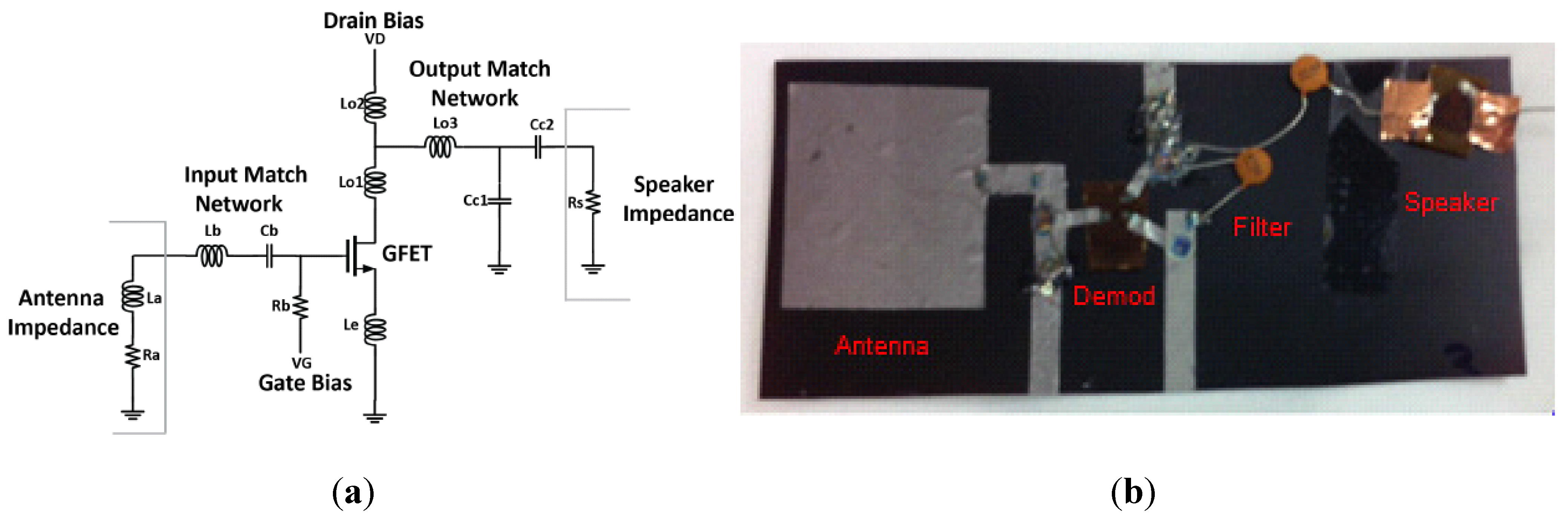
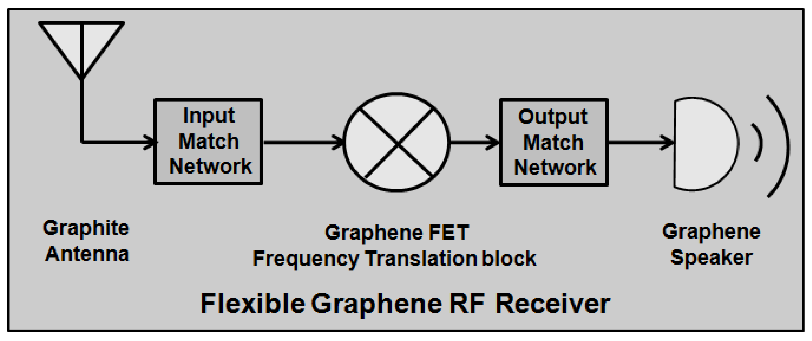
3.5. GFET Based Flexible Receiver

Figure 5 shows the block diagram of a relatively simple graphene based radio frequency communication system. It consists of a graphite antenna which receives the RF signal. This is followed by an input match network for impedance matching between the antenna and graphene based frequency translation block (mixer or demodulator) that function as an RF signal down-converter. The low frequency output of the frequency translation block or mixer is connected to a graphene speaker through an output matching network. In the following subsections we describe the realization of graphene RF communication circuits.
Figure 5. Schematic of a Flexible graphene based RF system.
Electronics 04 00933 g005

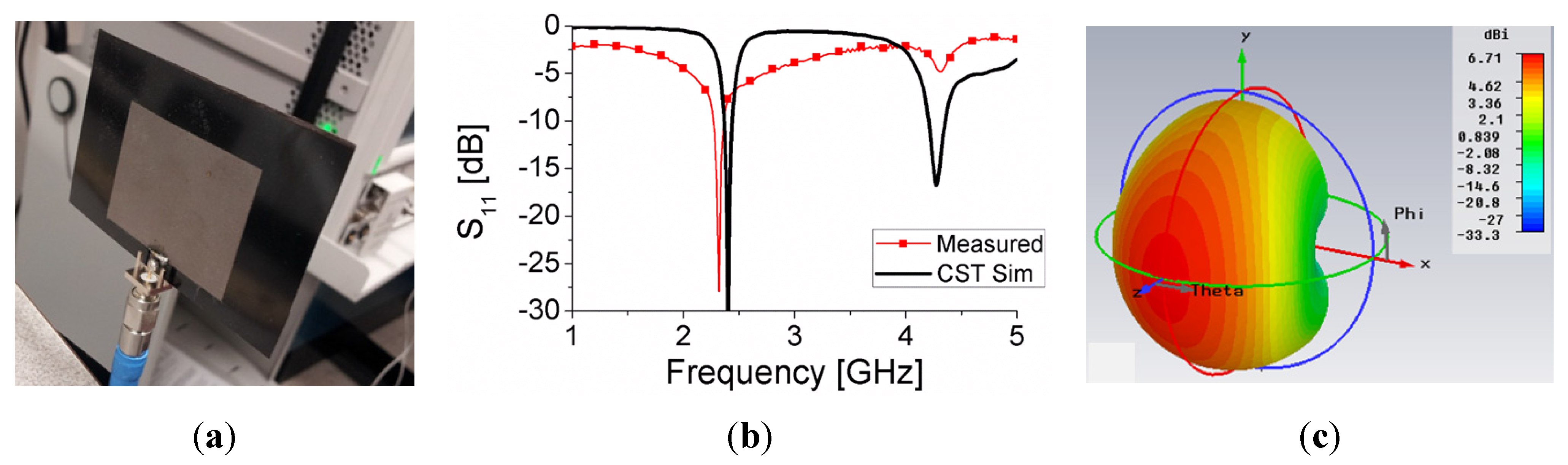
3.5.1. Graphite Flexible Antenna

We designed and fabricated a graphite based microstrip patch antenna at 2.4 GHz on flexible polyimide substrate (Figure 6a). The performance of this antenna is similar but relatively more lossy than copper based patch antenna. This antenna is designed towards the goal of achieving an all graphene/carbon flexible RF receiver system. The antenna was designed using a graphite sheet since it is more conductive than monolayer graphene at microwave frequencies [20]. Graphite sheets offer superior flexibility and thermal conductivity compared to copper, albeit lower electrical conductivity. It is expected that flexible planar antennas based on graphite sheets are compatible with roll to roll manufacturing for large-area or high volume applications. In addition, the DC conductivity of intercalated graphite antennas can be tuned for the design of sensors and reconfigurable RF systems [21]. The antenna simulation results from a 3D electromagnetic solver, (CST) and experimental measurements are shown in Figure 6b. The antenna dimensions are width W = 39.11 mm and length L = 30.95 mm. The far field radiation pattern is shown in Figure 6c.
Figure 6. (a) Graphite Patch Antenna; (b) Measured and simulated response; (c) Simulated radiation pattern (adapted from [17], Copyright 2013, permission granted by Kristen Parrish).
Electronics 04 00933 g006
To investigate the flexibility of the antenna, convex bending tests were carried out as shown in Figure 7a. The antenna was placed in the middle of a test vice fixture and mechanically bent (see Figure 7b). The S11 was measured in situ for each bending radius (see Figure 7c). The resonant frequency changes are relatively small down to ~30 mm bending radius. This result offers new opportunity for carbon/graphene RF electronics that can be integrated with flexible substrates, including bendable GHz electronics and antennas.
Figure 7. (a) Convex bending of graphite antenna; (b) Antenna is placed in the middle of test vice fixture; (c) Antenna response with convex bending of r = 29 mm (adapted from [17], Copyright 2013, permission granted by Kristen Parrish).
Electronics 04 00933 g007

3.5.2. Frequency Translation Block
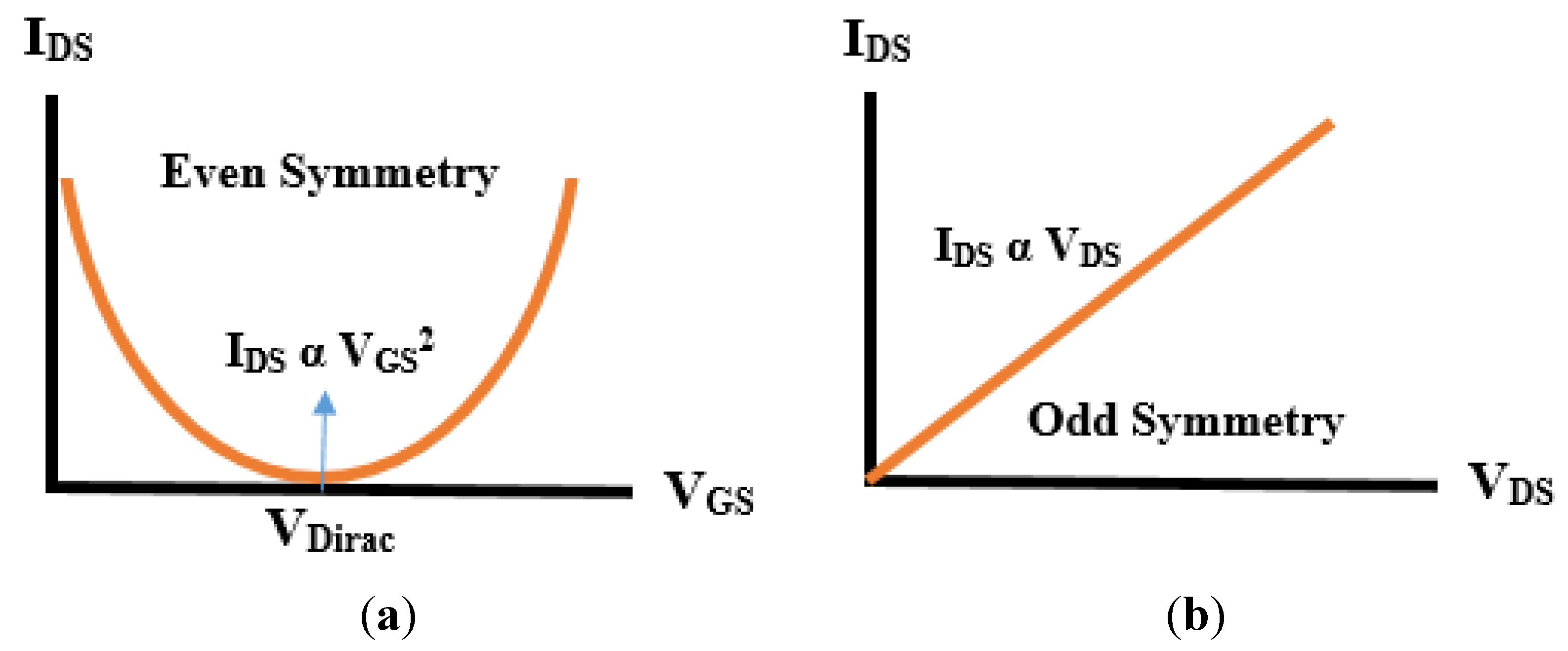
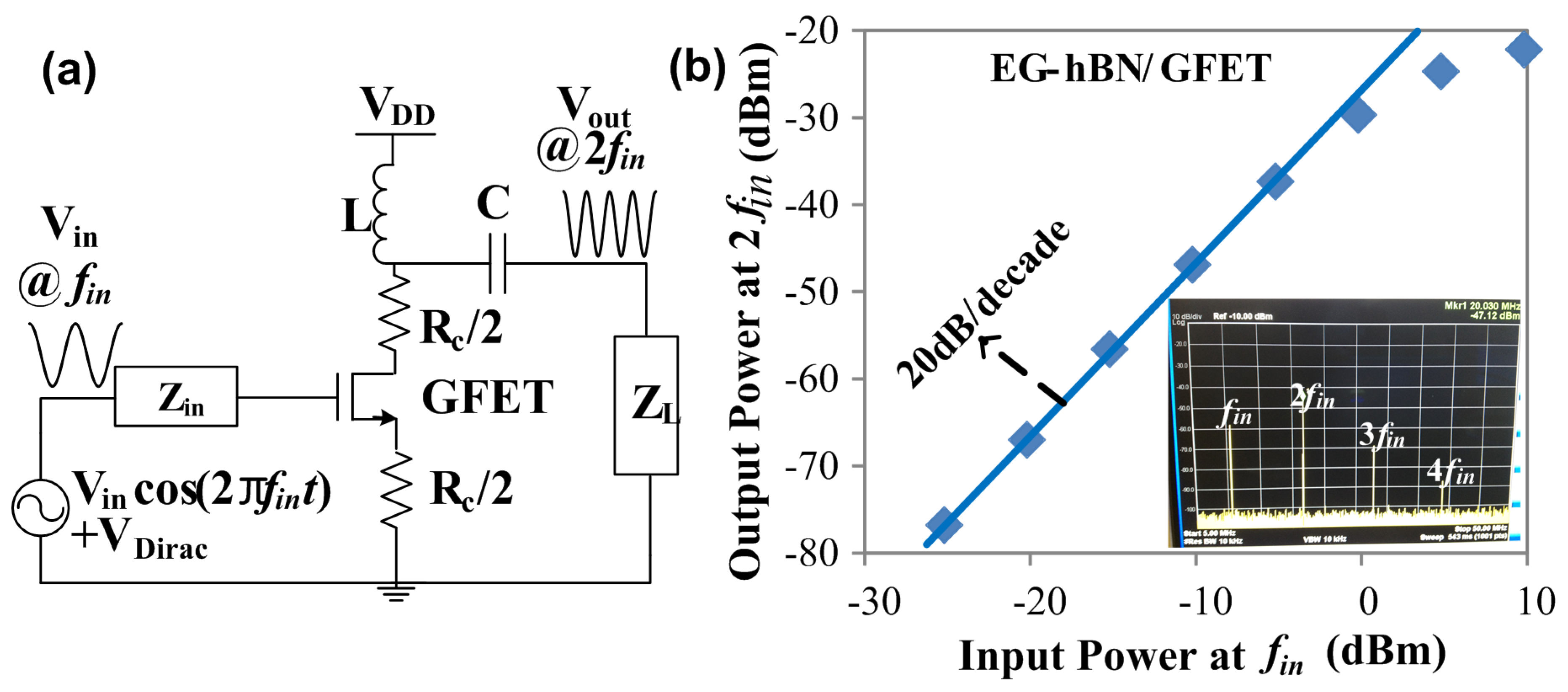
We describe in the following subsections two types of frequency translation blocks, GFET doublers and demodulators. GFET doubler is a frequency multiplier which can enable the realization of very high frequency communication circuits on soft substrates. On the other hand, a GFET demodulator described here does AM demodulation from carrier frequency to baseband. In general, graphene transistors can also be modified to serve as a demodulator for a variety of communication schemes, such as amplitude shift keying (ASK), frequency shift keying (FSK) and phase shift keying (PSK) modulations [13].

(1) GFET Doubler

We designed and fabricated a graphene doubler on flexible PI substrate. We will first discuss the operating principle of a GFET doubler. The input and output characteristics of an ideal square law transistor doubler are depicted in Figure 8.
Figure 8. (a) Transfer and (b) Output Characteristics of an ideal square law transistor doubler (adapted from [22], Copyright 2011, AIP Publishing LLC).
Electronics 04 00933 g008
It has ambipolar input characteristics (even symmetry) due to current conduction by both holes and electrons. For positive gate bias (VGS > Vdirac) electrons conduct and for negative gate bias (VGS < Vdirac) holes conduct. Ideally, the Dirac voltage should be around 0 V. The drain current IDS is proportional to VGS2. On the other hand, the output current characteristic is linear (odd symmetry) with respect to the drain bias, VDS. Using these two properties of an ideal square law device in our transistor model (Figure 2) we can derive an approximate expression for the output voltage:
  | v d s | =   g 0 R L γ V D S v i n 2 ( cos 2 ω i n t ) 2 n 0 + g 0 R L ( 2 n 0 + γ v i n 2 )
where g0 and γ are scaling factors, and RL is the load resistor. These parameters and coefficients are described in detail in our previous works [17,22].
In Equation (5) we have neglected higher order terms in the simplified analysis. This working description clearly shows that GFET biased at Dirac point can be used as a frequency doubler [17]. In practice, there are several sources of non-idealities that can degrade doubler performance including charged impurities and contact resistance with consequent reduction of electron-hole symmetry and gate modulation.
We fabricated a prototype GFET doubler biased at the Dirac point using the above concept. Figure 9a shows the schematic of the frequency doubler. A function generator is used to apply the RF input. Bias-Tees are used for input and output routing for DC bias, and an oscilloscope as the load to the doubler. Figure 9b shows the power spectrum. The conversion gain of our doubler is −29.5 dB [16]. This is relevant in the context of (flexible) RF transmitters which typically requires frequency upconversion.
Figure 9. (a) GFET Doubler; and (b) Power Spectrum (adapted from [16], Copyright 2013, permission granted by IEEE).
Electronics 04 00933 g009

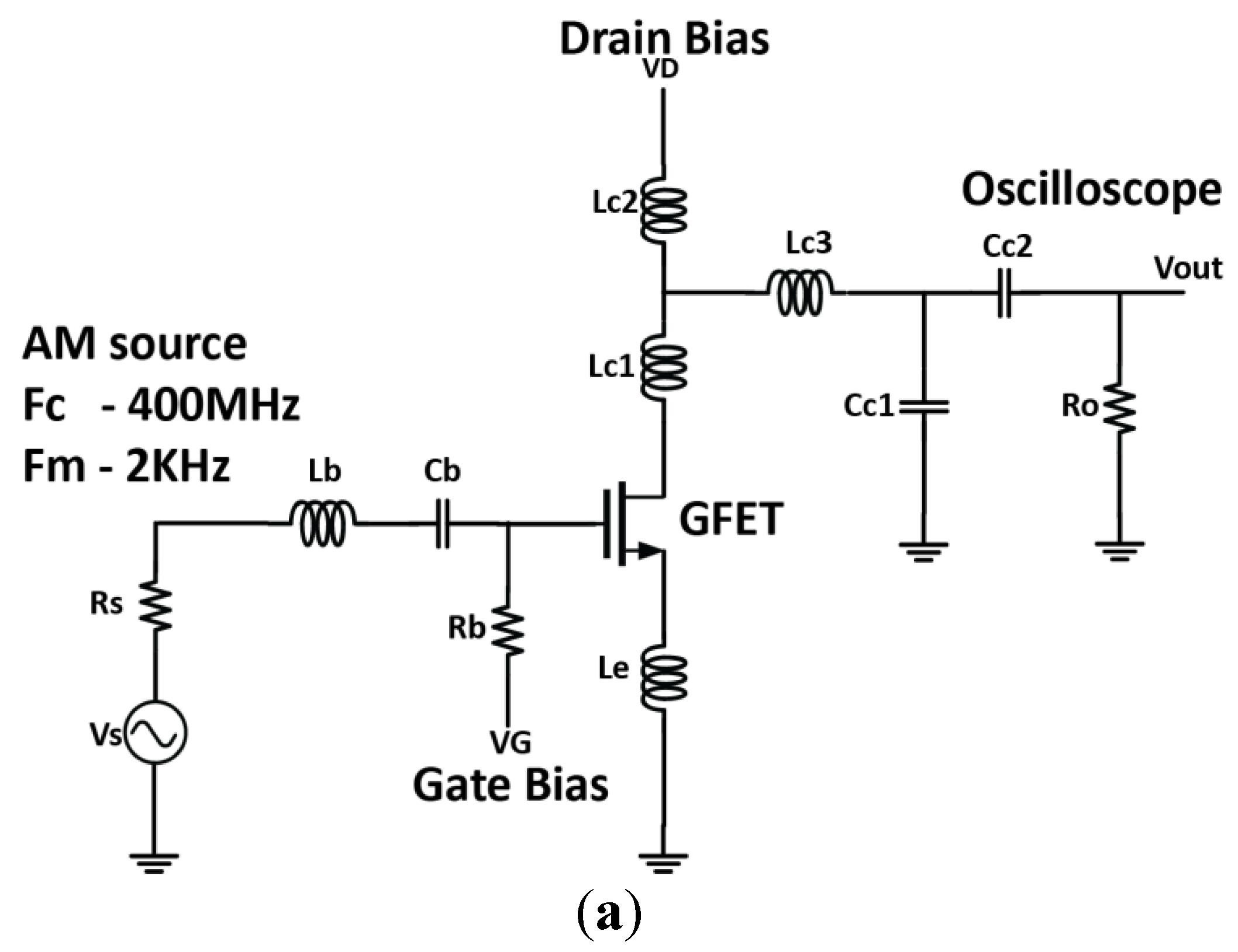
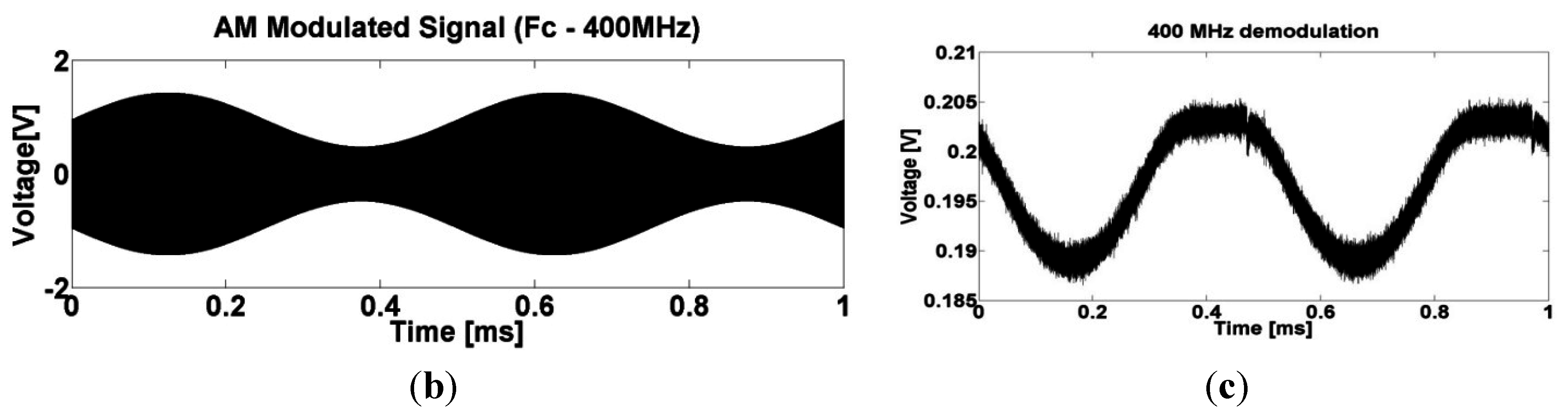
(2) GFET AM Demodulator

In our goal towards the demonstration of a flexible graphene AM radio, we designed and fabricated a flexible GFET demodulator. The demodulator circuit is as shown in Figure 10a. The input is an AM modulated signal (2 KHz modulation frequency, 400 MHz carrier frequency). The output is connected to an oscilloscope through a low pass filter. Smoothening capacitors are used at the output to limit the spectra to the audio range. The GFET is biased close to the Dirac point. The ambipolar characteristic of GFET at the Dirac point (see Equation (5)) makes it to act as a square law AM demodulator. Low pass filtering is necessary at output to filter out higher order harmonics that are also produced. The gain of the demodulator is ~−34 dB (Figure 10b,c). The gain performance is on the low end for the current devices due to parasitics from the source and drain contacts and interconnects. The GFET demodulator, resistors and capacitors (Cc1 and Cc2 surface mount device components) are mounted on the flexible polyimide substrate.
Figure 10. (a) GFET Demodulator (b) AM input and (c) Demod output (adapted from [17], Copyright 2013, permission granted by Kristen Parrish).
Electronics 04 00933 g010aElectronics 04 00933 g010b

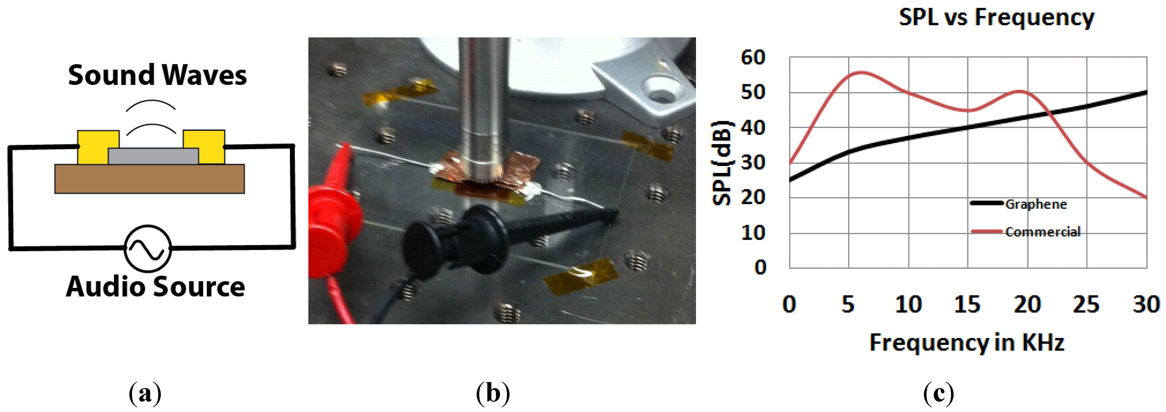
3.5.3. Flexible Graphene Speaker

Graphene along with its outstanding electrical and mechanical properties has very good thermal-acoustic characteristics. It offers very small heat capacity per unit area making it suitable as a thermo-acoustic speaker [23,24]. These graphene speakers are becoming quite attractive owing to its potentially low manufacturing cost, light weight, low power consumption and also high flexibility. Recently, Tian et al. demonstrated flexible graphene based speaker on a paper substrate [23,24]. In this light, we have designed and fabricated a flexible mono layer graphene speaker on PI substrate as shown in Figure 11. CVD grown monolayer graphene (1 cm2) is transferred onto a smoothened PI substrate. Gold/Silver metal contacts are deposited at the two edges of graphene. Baseband demodulated signal from receiver is applied to the two contacts. These signals create thermal oscillations at the graphene-air interface, which are then converted to sound waves.
Figure 11. (a) Side view of graphene speaker (grey—monolayer graphene, yellow—gold contacts, brown—PI substrate); (b) Fabricated graphene speaker and microphone test setup; (c) SPL vs. frequency plot comparing flexible graphene speaker with a commercial speaker. (adapted from [25], Copyright 2014, IEEE)
Electronics 04 00933 g011
The measurement of the sound waves from this speaker is performed using a microphone and signal analyzer (See Figure 11b). The distance between the microphone and speaker is kept at 3 cm. This speaker performance is as shown in Figure 11c. It also shows the comparison with commercial speaker. These speakers provide a sound pressure level (SPL) of 25–50 dB in the audio frequency range. The speaker power at high frequencies is given by Equation (6) [23]. It mainly depends on frequency of sound (f), heat capacity of air (γ), velocity of sound in air (vg) thermal effusivity of PI substrate (es) and air (ea) [23].
P s p e a k e r =   R o   2 r o   γ 1 v g e g e s + a c + e g q o
Future research towards monolithic graphene nanosystems requires integration of the speaker with the AM radio receiver. The performance of this speaker at low frequency can be improved by high quality graphene film, waveguide design and fabrication of suspended graphene speakers.

3.5.4. Graphene AM Radio Receiver

A graphene based flexible AM radio receiver at 2.4 GHz was designed and fabricated based on the block diagram of Figure 9. The receiver consists of a graphite antenna, GFET demodulator and speaker. The receiver is fabricated on a polyimide flexible substrate. The AM input signal is obtained from a signal generator (2.45 GHz carrier signal) and transmitted by a horn antenna. The signal is received by the graphite antenna and demodulated using the GFET demodulator based on the ambipolar graphene characteristics at the Dirac point. The output of the demodulator is connected to the speaker [25].
The schematic of the AM radio receiver is shown in Figure 12a. The input matching network is used for impedance matching between the antenna (La, Ra) and GFET input impedance. The output matching network has two functions: (i) impedance match between output of GFET and graphene speaker load (Ro) and (ii) low pass filtering of the demodulated signal. Figure 12b shows the fabricated receiver. The passive components—inductors, capacitors and resistors are currently realized using surface mount device (SMD) components. The receiver measurements were carried out in a custom built anechoic chamber. Bending tests (~30 mm radius) were successfully carried out. The performance changes are small due to the flexibility of substrate, antenna, graphene FET and transmission lines.
Figure 12. (a) Schematic of a graphene-based AM radio receiver; (b) Fabricated AM radio receiver on a flexible PI (Kapton) substrate (adapted from [25], Copyright 2014, IEEE)
Electronics 04 00933 g012
The link budget of the flexible graphene receiver is estimated to be −46dB. In this estimation we have considered path loss to be −1dB/cm for 6cm signal propagation through air, graphite antenna loss to be 5dB, and GFET demodulator circuit gain to be -35dB. The current AM receiver suffers from very high noise output due to lossy (un-optimized) demodulator. To obtain larger signal to noise ratio and amplitude, a GFET low noise amplifier could be incorporated at the input. The performance could be further improved with optimized design of the demodulator and interconnects.

4. Conclusions

In this article on the research progress towards flexible integrated graphene nanosystems, we demonstrate the feasibility of an all graphene/carbon flexible RF communication receiver. We have shown state of the art flexible GFET with high cutoff frequency in the microwave GHz regime. We have also investigated the realization and performance of GFET doubler and demodulator, flexible graphene speaker, flexible graphite antenna and carbon based AM receiver. Improved receiver performance can be achieved with the use of semiconducting layered atomic materials such as MoS2 and black phosphorous for high-gain baseband amplifiers and mixed signal circuits.

Acknowledgments

This work is supported in part by the Office of Naval Research (ONR) and the National Science Foundation (NSF) Nascent Engineering research center (ERC) under Cooperative Agreement No. EEC-1160494. The research was carried out at the Microelectronics Research Center at The University of Texas at Austin. We acknowledge the help of He Tian and Tian-Ling Ren of Tsinghua University with graphene speaker measurements.

Author Contributions

All authors contributed to the research described in this work. M.N.Y., K.N.P., J.L., D.A conceived and designed the experiments; M.N.Y., K.N.P. S.P. performed the experiments; M.N.Y. and K.N.P. analyzed the data; M.N.Y., D.A. wrote the paper.

Conflicts of Interest

The authors declare no conflict of interest.

References

  1. Russer, P.; Fitchner, N. Nanoelectronoics in Radio Frequency technology. IEEE Microw. Mag. 2010, 11, 119–135. [Google Scholar] [CrossRef]
  2. Akinwande, D.; Petrone, N.; Hone, J. Two-dimensional flexible nanoelectronics. Nat. Commun. 2014, 5. [Google Scholar] [CrossRef] [PubMed]
  3. Schwierz, F. Graphene Transistors: Status, Prospects, and Problems. Proc. IEEE 2013, 101, 1567–1584. [Google Scholar] [CrossRef]
  4. Akinwande, D.; Tao, L.; Yu, Q.; Lou, X.; Peng, P.; Kuzum, D. Large-Area Graphene Electrodes: Using CVD to facilitate applications in commercial touchscreens, flexible nanoelectronics, and neural interfaces. Nanotechnol. Mag. IEEE 2015, 9, 6–14. [Google Scholar] [CrossRef]
  5. Yeh, C.-H.; Lain, Y.-W.; Chiu, Y.-C.; Liao, C.-H.; Moyano, D.R.; Hsu, S.S.H.; Chiu, P.-W. Gigahertz Flexible Graphene Transistors for Microwave Integrated Circuits. ACS Nano 2014, 8, 7663–7670. [Google Scholar] [CrossRef] [PubMed]
  6. Nathan, A.; Ahnood, A.; Cole, M.T.; Sungsik, L.; Suzuki, Y.; Hiralal, P.; Bonaccorso, F.; Hasan, T.; Garcia-Gancedo, L.; Dyadyusha, A.; et al. Flexible Electronics: The Next Ubiquitous Platform. Proc. IEEE 2012, 100, 1486–1517. [Google Scholar] [CrossRef]
  7. Kim, D.H.; Lu, N.; Ma, R.; Kim, Y.S.; Kim, R.-H.; Wang, S.; Wu, J.; Won, S.M.; Tao, H.; Islam, A.; et al. Epidermal Electronics. Science 2011, 333, 838–843. [Google Scholar] [CrossRef] [PubMed]
  8. Lee, J.; Ha, T.; Li, H.; Parrish, K.N.; Holt, M.; Dodabalapur, A.; Ruoff, R.S.; Akinwande, D. 25 GHz Embedded-Gate Graphene Transistors with High-K Dielectrics on Extremely Flexible Plastic Sheets. ACS Nano 2012, 7. [Google Scholar] [CrossRef] [PubMed]
  9. Chang, H.; Yang, S.; Lee, J.; Tao, L.; Hwang, W.; Jena, D.; Lu, N.; Akinwande, D. High-Performance, Highly Bendable MoS2 Transistors with High-K Dielectrics for Flexible Low-Power Systems. ACS Nano 2013, 7, 5446–5452. [Google Scholar] [CrossRef] [PubMed]
  10. Li, X.; Cai, W.; An, J.; Kim, S.; Nah, J.; Yang, D.; Piner, R.; Velamakanni, A.; Jung, I.; Tutuc, E.; et al. Large-area synthesis of high-quality and uniform graphene films on copper foils. Science 2009, 324, 1312–1314. [Google Scholar] [CrossRef] [PubMed]
  11. Wang, H.; Hsu, A.L.; Palacios, T. Graphene electronics for RF applications. Microw. Mag. IEEE 2012, 13, 114–125. [Google Scholar] [CrossRef]
  12. Han, S.; Garcia, A.V.; Oida, S.; Jenkins, K.A.; Haensch, W. Graphene radio receiver integrated circuit. Nat. Commun. 2014, 5. [Google Scholar] [CrossRef] [PubMed]
  13. Lee, S.; Lee, K.; Liu, C.; Kulkarni, G.S.; Zhong, Z. Flexible and transparent all-graphene circuits for digital quaternary modulations. Nat. Commun. 2012, 3. [Google Scholar] [CrossRef] [PubMed]
  14. Park, S.; Zhu, W.; Chang, H.-Y.; Yogeesh, M.N.; Ghosh, R.; Banerjee, S.; Akinwande, D. High-frequency prospects of 2D nanomaterials for flexible nanoelectronics from baseband to sub-THz devices. In Proceedings of the 2015 IEEE International Electron Devices Meeting (IEDM) Technical Digest, Washington, DC, USA, 7–9 December 2015; pp. 32.1.1–32.1.4.
  15. Parrish, K.N.; Ramón, M.E.; Banerjee, S.K.; Akinwande, D. A Compact Model for Graphene FETs for Linear and Non-linear Circuits. In Proceedings of the SISPAD 2012, Denver, CO, USA, 5–7 September 2012.
  16. Lee, J.; Ha, T.J.; Parrish, K.N.; Chowdhury, SF.; Tao, L.; Dodabalapur, A.; Akinwande, D. High performance current saturating graphene field-effect transistor with hexagonal boron nitride dielectric on flexible polymeric substrates. IEEE Electron Device Lett. 2013, 34, 172–174. [Google Scholar] [CrossRef]
  17. Parish, K. Nanoscale Graphene for RF Circuits and System. Ph.D. Dissertation, University of Texas at Austin, Austin, TX, USA, August 2013. [Google Scholar]
  18. Koolen, M.C.A.M.; Geelen, J.A.M.; Versleijen, M.P.J.G. An Improved De-Embedding Technique for on-Wafer High-Frequency Characterization. In Proceedings of the IEEE 1991 Bipolar Circuits and Tech Meeting, Minneapolis, MN, USA, 9–10 September 1991.
  19. Lee, J. Graphene Field Effect Transistors for Flexible High Frequency Electronics. Ph.D. Dissertation, University of Texas at Austin, Austin, TX, USA, May 2013. [Google Scholar]
  20. Panasonic PGS Graphite Sheets. Available online: http://industrial.panasonic.com/lecs/www-data/pdf/AYA0000/AYA0000CE2.pdf (accessed on 30 June 2014 ).
  21. Ferendeci, A.; Devlin, C.L.H. Microwave Charecterization of Graphite and Intercalated Graphite as an Antenna Element. In Proceedings of the 2012 IEEE National Aerospace and Electronics Conference (NAECON), Dayton, OH, USA, 25–27 July 2012.
  22. Parrish, K.N.; Akinwande, D. Even-odd symmetry and the conversion efficiency of ideal and practical graphene transistor frequency multipliers. Appl. Phys. Lett. 2011, 99, 223512. [Google Scholar] [CrossRef]
  23. Tian, H.; Ren, T.; Xie, D.; Wang, Y.; Zhou, C.; Feng, T.; Fu, D.; Yang, Y.; Peng, P.; Wang, L.; et al. Graphene-on-Paper sound source devices. ACS Nano 2011, 5, 4878–4885. [Google Scholar] [CrossRef] [PubMed]
  24. Suk, J.W.; Kirk, K.; Hao, Y.; Hall, N.A.; Ruoff, R.S. Thermoacoustic sound generation from monolayer graphene for transparent and flexible sound sources. Adv. Mater. 2012, 24, 6342–6347. [Google Scholar] [CrossRef] [PubMed]
  25. Yogeesh, M.N.; Parrish, K.N.; Lee, J.; Tao, L.; Akinwande, D. Towards the design and fabrication of graphene based flexible GHz radio receiver systems. In Proceedings of the 2014 IEEE MTT-S International Microwave Symposium (IMS), Tampa, FL, USA, 1–6 June 2014.

