Article

Electrical Reliability of a Film-Type Connection during Bending

Japan Aviation Electronics Ind., Ltd., 3-1-1, Musashino, Akishima, Tokyo 196-8555, Japan
*
Author to whom correspondence should be addressed.
Electronics 2015, 4(4), 827-846; https://doi.org/10.3390/electronics4040827
Submission received: 13 July 2015 / Revised: 17 October 2015 / Accepted: 17 October 2015 / Published: 26 October 2015
(This article belongs to the Special Issue Flexible Electronics)

Abstract

:
With the escalating demands for downsizing and functionalizing mobile electronics, flexible electronics have become an important aspect of future technologies. To address limitations concerning junction deformation, we developed a new connection method using a film-type connector that is less than 0.1 mm thick. The film-type connector is composed of an organic film substrate, a UV-curable adhesive that deforms elastically under pressure, and electrodes that are arranged on the adhesive. The film-type connection relies on a plate-to-plate contact, which ensures a sufficient contact area. The electrical reliability of the film-type connection was investigated based on changes in the resistance during bending at curvature radii of 70, 50, 25, 10, 5, and 2.5 mm. The connection was bent 1000 times to investigate the reproducibility of the connector’s bending properties. The tests showed that no disconnections occurred due to bending in the vertical direction of the electrode, but disconnections were observed due to bending in the parallel direction at curvature radii of 10, 5, and 2.5 mm. In addition, the maximum average change in resistance was less than 70 milliohms unless a disconnection was generated. These results support the application of the new film-type connection in future flexible devices.

Graphical Abstract

1. Introduction

To create smaller, thinner, lighter, and shorter miniature mobile devices while retaining high functionality as well as securing space for a battery inside the device, the demand for high-density packaging has been increasing and has become difficult to address. Of the variety of available packaging approaches, electrical connections using flexible printed circuits (FPCs) represent one of the most important technologies for meeting these demands due to their beneficial properties such as their marginal weight, thinness, and flexible form factors [1,2]. In general, a dedicated connector or anisotropic conductive film (ACF) is used to connect FPCs to printed circuits and other electronic components. When using a connector, conduction between the facing FPC electrode and the connector electrode relies on a mechanical normal force [3]; thus, mechanical designs for miniaturized connectors are limited by the requirement for a sufficient normal force.
ACFs are film-type adhesives that are made of a thermosetting resin in which conductive particles have been dispersed. During the connection process, heat and pressure are applied to the film between the FPC electrode and the connecting electrode, which results in conduction through the conductive particles between the electrodes, and the hardening shrinkage of the resin maintains the connected state. This approach is superior to using a connector because the height of the packaging can be significantly decreased, and appropriately selecting the type of conductive particles, their diameter, and the dispersion state can allow for applications with connections across fine gaps. Using this method, ACFs have become an essential component for the assembly of flat panel display modules [4,5,6].
Conversely, flexible electronics, the common name for the fundamental set of technologies that are related to devices that are flexible and bendable, have recently become popular [7,8,9,10,11,12,13,14,15,16,17,18,19,20,21,22,23,24,25,26,27,28,29,30,31,32,33,34,35,36,37,38,39,40,41]. Many applications of flexible electronics, including displays [9,10,11], sensors [12,13,14], batteries [15,16,17], solar cells [18,19,20], memory [21,22,23], and radio frequency identification (RFID) tags [24,25,26], have been proposed. In these applications, device functionality is enhanced by (1) providing portability, impact resistance, and freedom of form; (2) reducing the weight and thickness of the device; and (3) providing novel operability through signal input methods using the bendability of the device itself, which improves the ease of use of the device via its flexibility. In particular, applications in the medical and healthcare fields that are synergistic with the concept of spiritual wellness have also become popular [27,28,29]. The use of roll-to-roll printing technologies enables low-cost manufacturing and large area compatibility [30,31].
Although many flexible devices have been developed, and although their flexibility has been investigated through cyclic bending tests [32,33,34,35,36,37,38,39,40,41], little attention has been paid to suitable packaging technologies for these devices. Packaging has stagnated due to the reuse of existing technologies, such as connectors and ACFs; however, there is a question about whether these existing technologies are sufficient. As mentioned previously, the approaches that follow the traditional method of miniaturizing and thinning existing conductors are limited because they involve applying rigid connectors to flexible devices, which sacrifices the flexibility of the device. In addition, when using ACFs, heat and pressure must be applied during connection, which may cause problems such as wiring gap misalignment caused by the deformation of the organic films that are used as the device substrate. As substrate films become thinner and as softer materials with good biocompatibility but poor thermal stability are increasingly used as substrates, we can assume that this misalignment problem will become more prominent. To address these issues, we developed a new connection technology with a film-type connector for use in flexible device packaging. The proposed film-type connector is composed of an organic film substrate, a UV-curable adhesive that deforms elastically with pressure, and electrodes that are arranged on the adhesive. Through the use of the UV-curable adhesive, the requirement for heating the adhesive is eliminated, which removes the risk of damage to the devices due to heat. In addition, the film-type connection produces a plate-to-plate contact between the electrodes and a connecting counter member, which ensures a sufficient contact area even under bending conditions. The results of a previous study demonstrated that the film-type connector has several advantages compared to ACFs regarding the mildness of the connection condition and the resistance stability of the contact in temperature/humidity aging tests, thermal cycling tests, and a preliminary flexibility test [42]. In this study, we describe additional investigations of the electrical reliability of the film-type connector under repeated bending conditions.

2. Methods

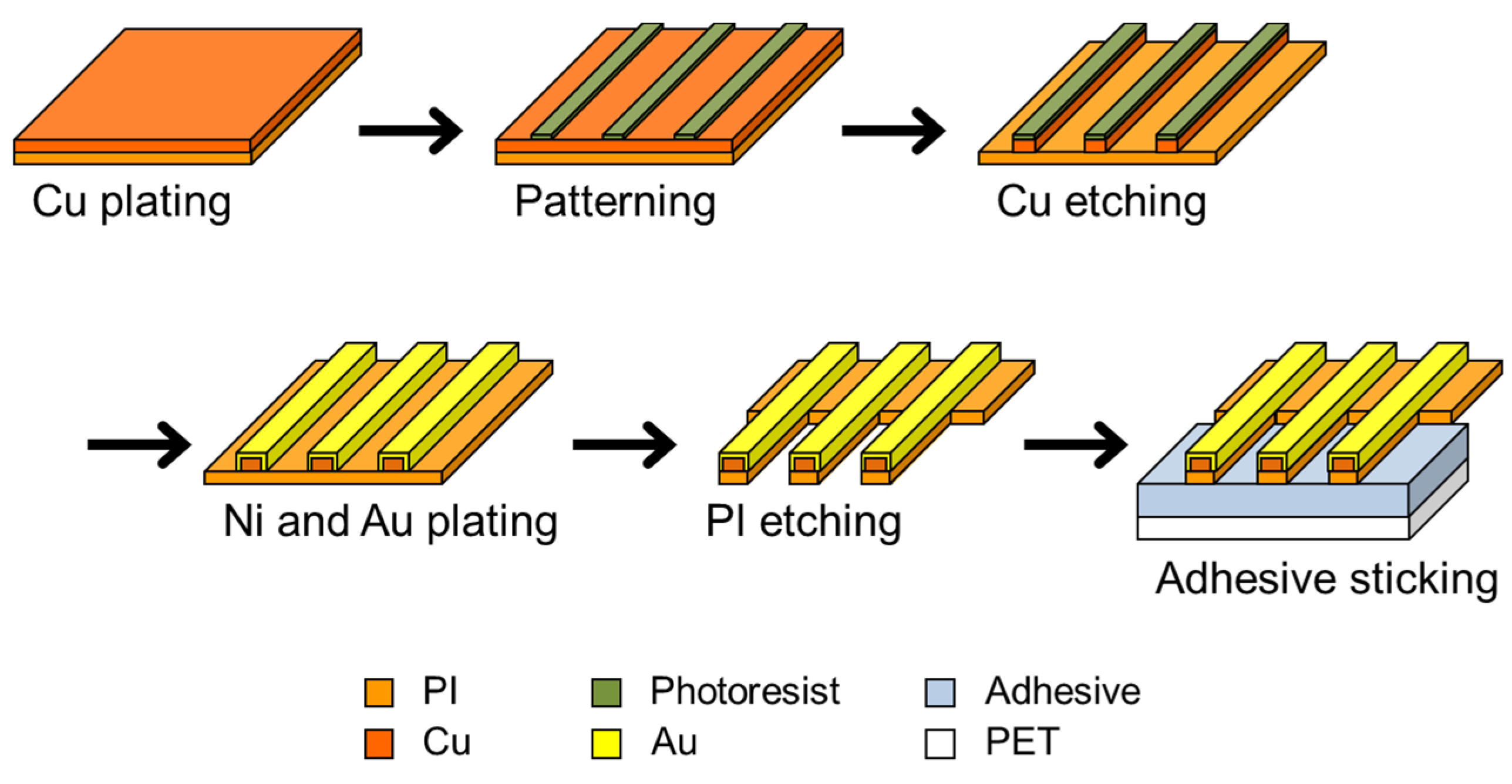
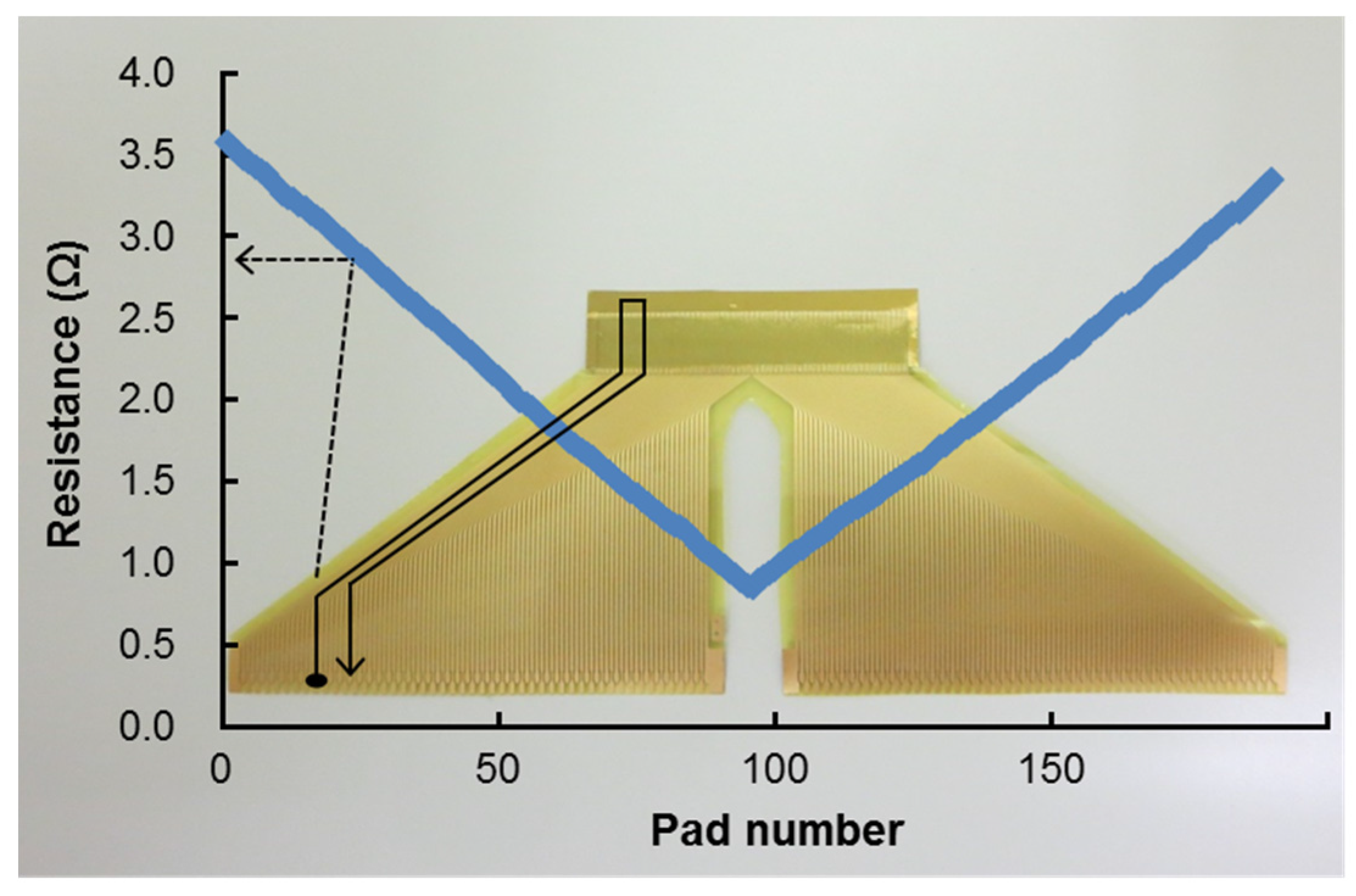
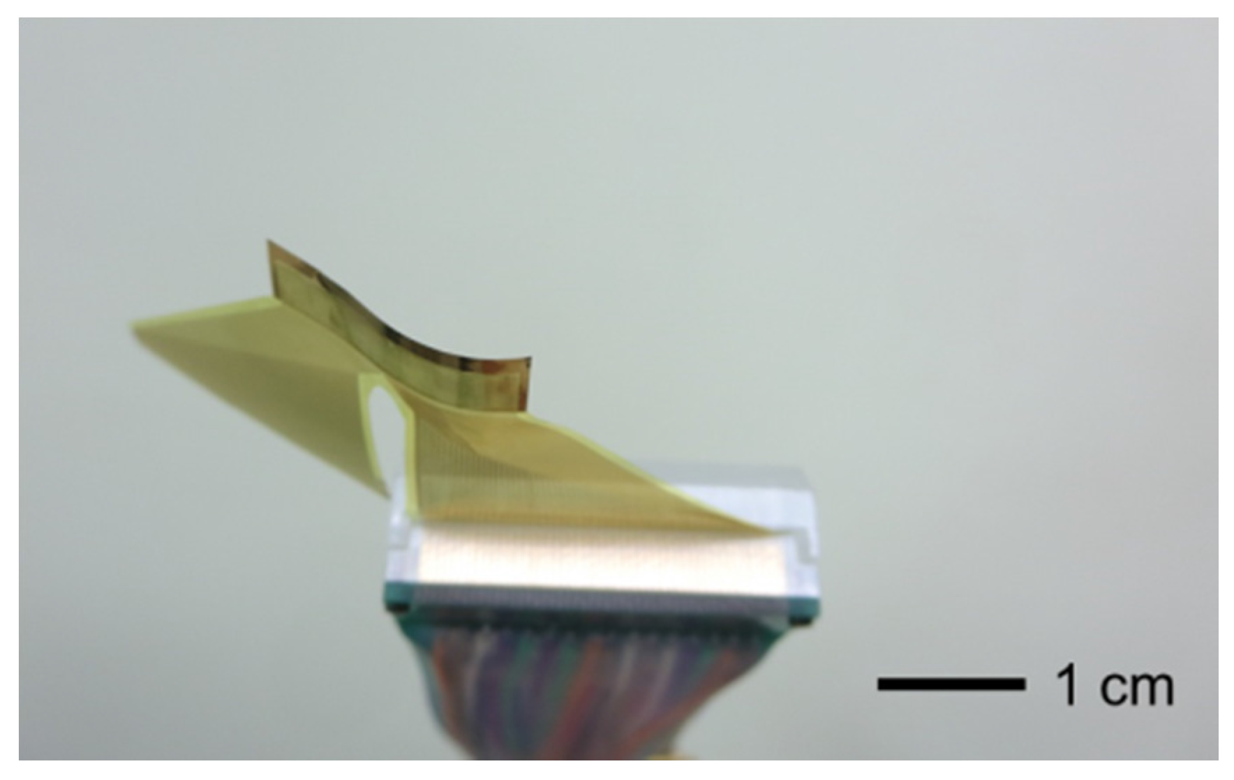
2.1. Fabrication of the Film-Type Connector

The film-type connector structure is basically the same as a single-sided FPC with a junction that contains an electrode that is located on the adhesive. Figure 1 shows the fabrication process of the film-type connector. First, a polyimide (PI) film was plated with copper, and anisotropic etching using a photolithographic process was then applied to form a pattern in the copper. After resist stripping with iron (II) chloride, nickel/gold plating was used to form the wiring. Finally, anisotropic etching of the PI film junction area was patterned in the same configuration as the electrode, and the adhesive on the poly(ethylene terephthalate) (PET) was laminated to the PI film side.
Figure 1. Fabrication scheme used to produce the film-type connector.
Electronics 04 00827 g001

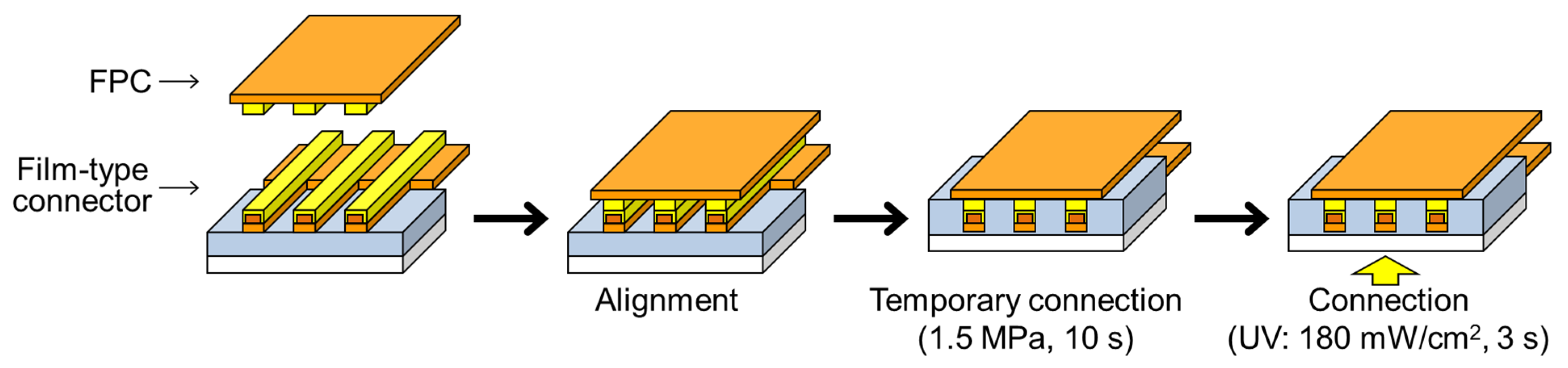
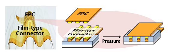
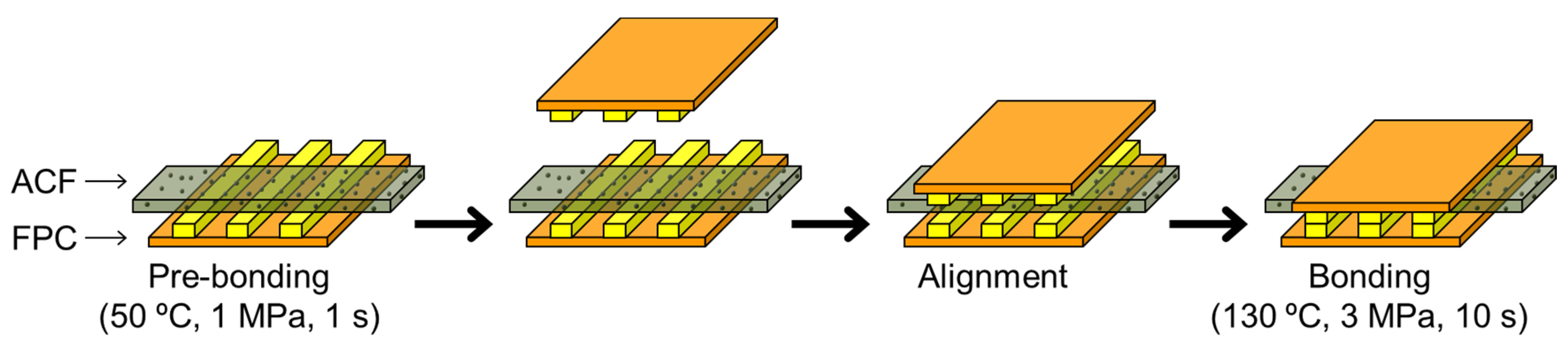
2.2. Connection Process of the Film-Type Connector

Figure 2 shows the connection process using the film-type connector with an FPC. The connection process consisted of a temporary adhesion process and a UV irradiation process. In the temporary adhesion process, the film-type connector electrode and the FPC electrode were aligned, and a pressure of 1.5 MPa was applied at room temperature for 10 s. As a result, the adhesive was pushed out from between the film-type connector electrode when the film was adhered to the FPC substrate, thereby ensuring conduction between the electrodes. After conduction was confirmed, a 365 nm, mid-wavelength, high-pressure mercury lamp with an irradiation intensity of 180 mW/cm2 was applied for 3 s to irradiate the connector with UV light at an intensity of 540 mJ/cm2 to cure the adhesive and increase the adhesive strength.
Figure 2. Connection process of the film-type connection.
Electronics 04 00827 g002

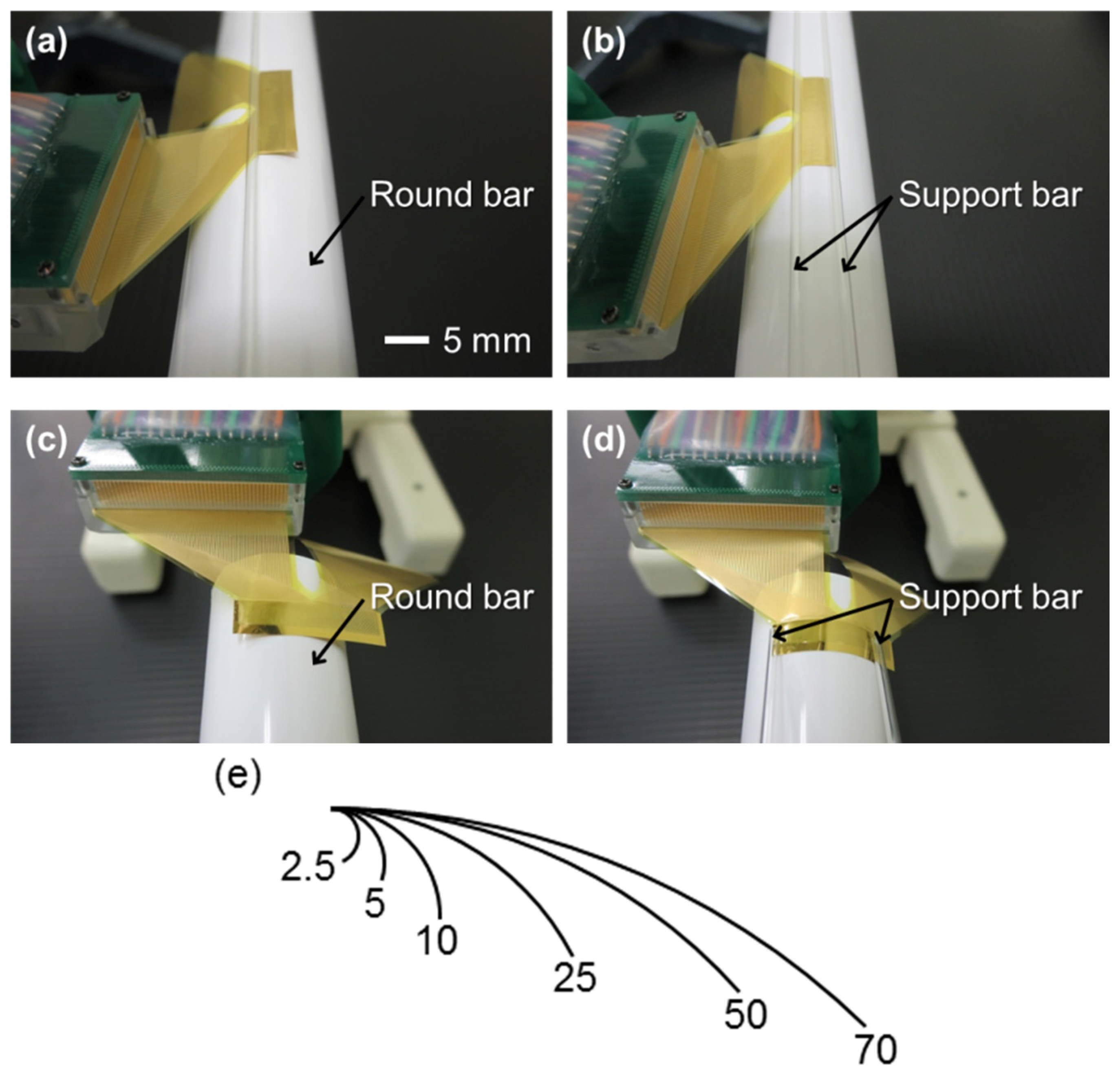
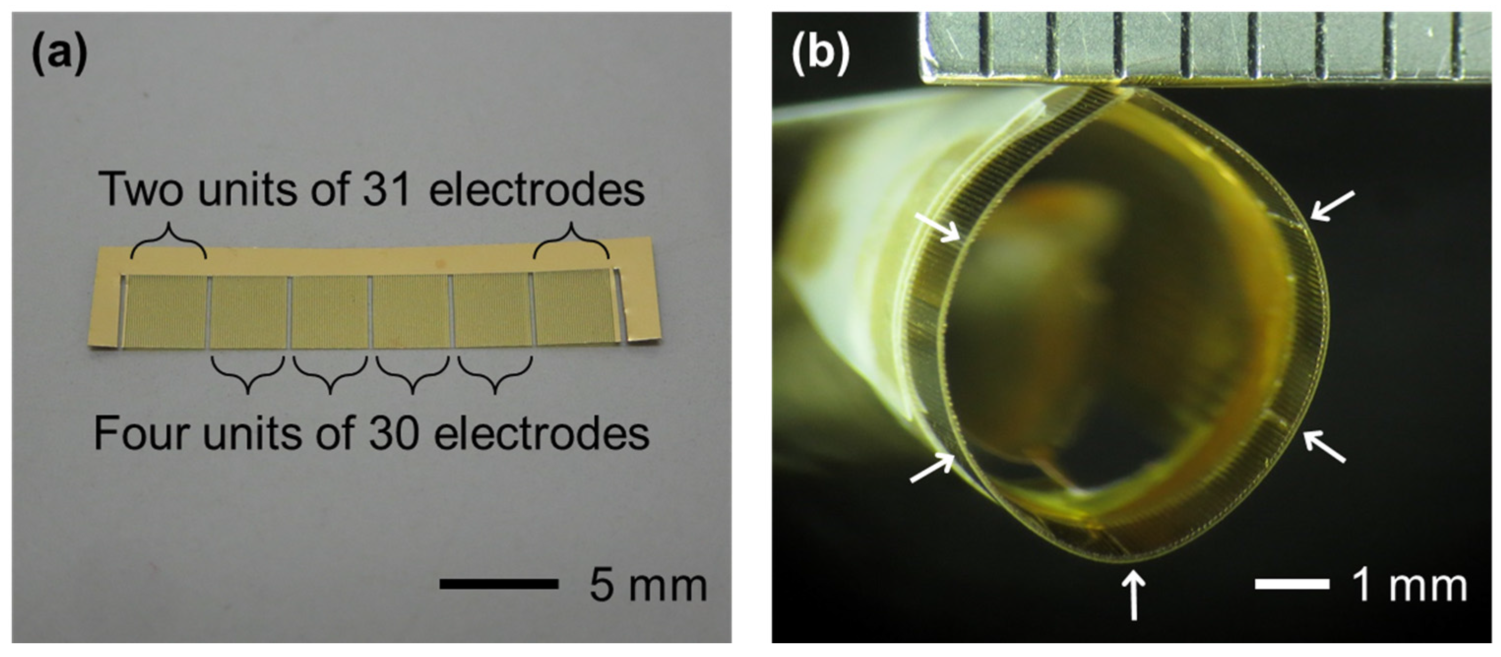
2.3. Preparation of Samples
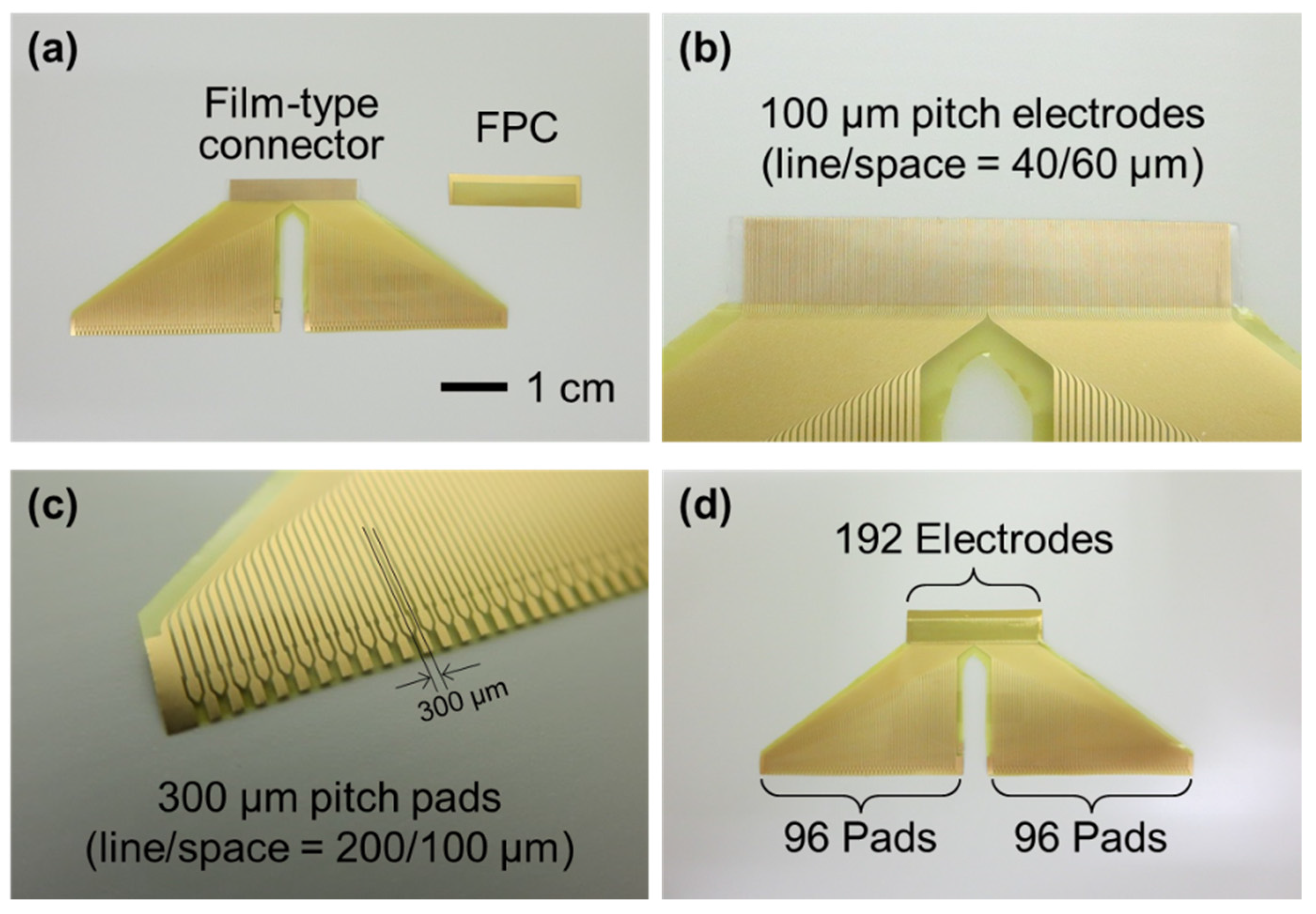
Figure 3 and Table 1 show the appearance and specifications of the samples that were used in this study. The film-type connector has straight electrodes that connect to an FPC that is assisted by the adhesive and zigzag pads that connect to the measuring instrument. A total of 192 electrodes were converted and divided into two units of 96 pads each to enable the bending of the junction. The FPC consisted of the same material as that of the film-type connector and was fabricated using the same process as the film-type connector except for the PI etching and adhesive sticking processes. The film-type connector was connected as shown in Figure 2.
Figure 3. Photographs of the film-type connection: (a) the film-type connector and the FPC; (b) electrodes; (c) pads; and (d) connected sample.
Electronics 04 00827 g003
Table 1. Specifications of the film-type connector.
DescriptionSpecification
PI film thickness7.5 µm
Electrode thicknessCu/Ni/Au = 9/0.5/0.1 µm
Electrode pitch100 µm (line/space = 40/60 µm)
Number of electrodes192
Adhesive thickness50 µm
PET substrate thickness25 µm

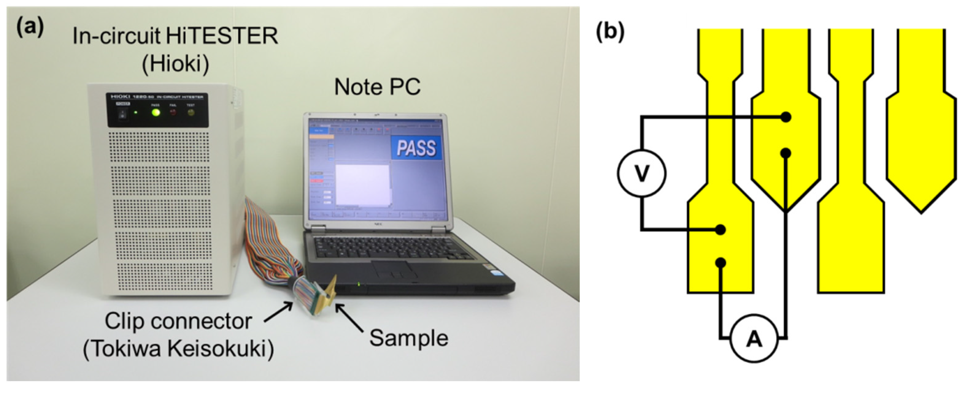
2.4. Measurement of the Electrical Resistance of the Samples

Figure 4a presents a photograph of the measuring system that was used in this study. A 96-pad unit of the film-type connector was connected to an in-circuit HiTESTER (Hioki E.E. Corp., Nagano, Japan) through a clip connector (Tokiwa Keisokuki Co., Ltd., Tokyo, Japan). Two electrodes of the clip connector were connected to each pad to measure the resistance using the four-point probe method, as shown in Figure 4b. A constant DC current of 20 mA was applied to the circuit, and the resistance was then measured. The changes in resistance were calculated by subtracting the initial resistance from the measured values and then averaging over all of the measurement data from the samples. The change in resistance includes the change in contact resistance and the change in wiring resistance. Measurements that involved the disconnection of the junction were excluded from the calculation.
Figure 4. Measuring system: (a) photograph of the system and (b) schematic of the four-point probe method.
Electronics 04 00827 g004

2.5. Procedure of the Bending Test

Using a sample that was connected to the FPC in the same manner as described in the previous section, we observed the change in resistance when the junction was bent at several curvature radii. During the bending tests, the resistance of one unit of a connected sample was measured due to the freedom in the bending. We measured the resistance first in the unbent state and then in bent states at curvature radii of 70, 50, 25, 10, 5, and 2.5 mm. After these measurements, the junction was returned to a flat state, and the resistance was then measured to calculate the change in resistance from the initial state (continuous measurement). The junction was bent 1000 times to investigate the repeated bending properties of the connection. The change in resistance was measured in the unbent state after performing different numbers of bending cycles (intermittent measurements). The connection that used the film-type connector did not have a symmetrical cross-section for the junction; thus, we conducted concave and convex bending tests with respect to the X- and Y-axes, respectively, as shown in Figure 5.
Figure 5. Schematic of the bending directions.
Electronics 04 00827 g005
Figure 6. Bending test methodology: (a,b) photographs before and after bending about the X-axis; (c,d) photographs before and after bending about the Y-axis; and (e) actual size of the curvature radii (units: mm).
Electronics 04 00827 g006
Figure 6a–d show photographs of the convex bending test for a curvature radius of 10 mm. By using support bars to press the sample to a round bar at each radius of curvature, uniform bending deformation could be generated. Although several methods of bending have been proposed, we used this method to minimize the forces that are not related to bending. Using a bending die can change the connection between the film-type connector and the FPC due to the direct application of external force to the connection. Moreover, some tension must be constantly applied to the sample. The actual size of each bending radius is shown in Figure 6e.

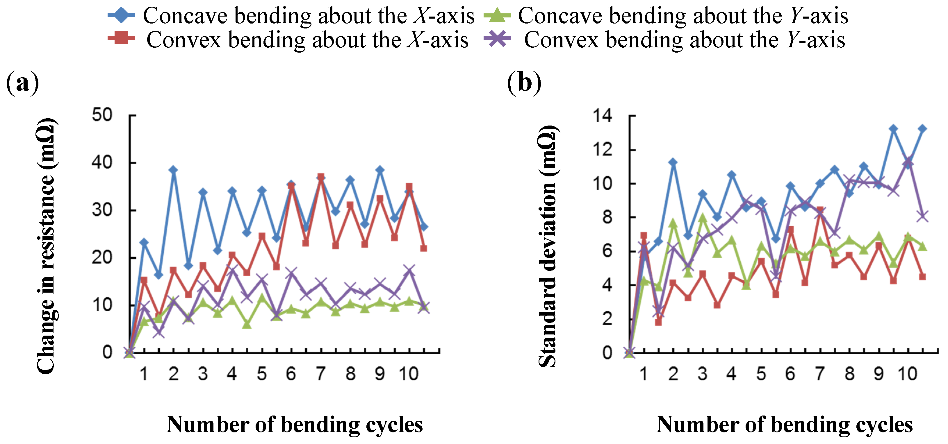
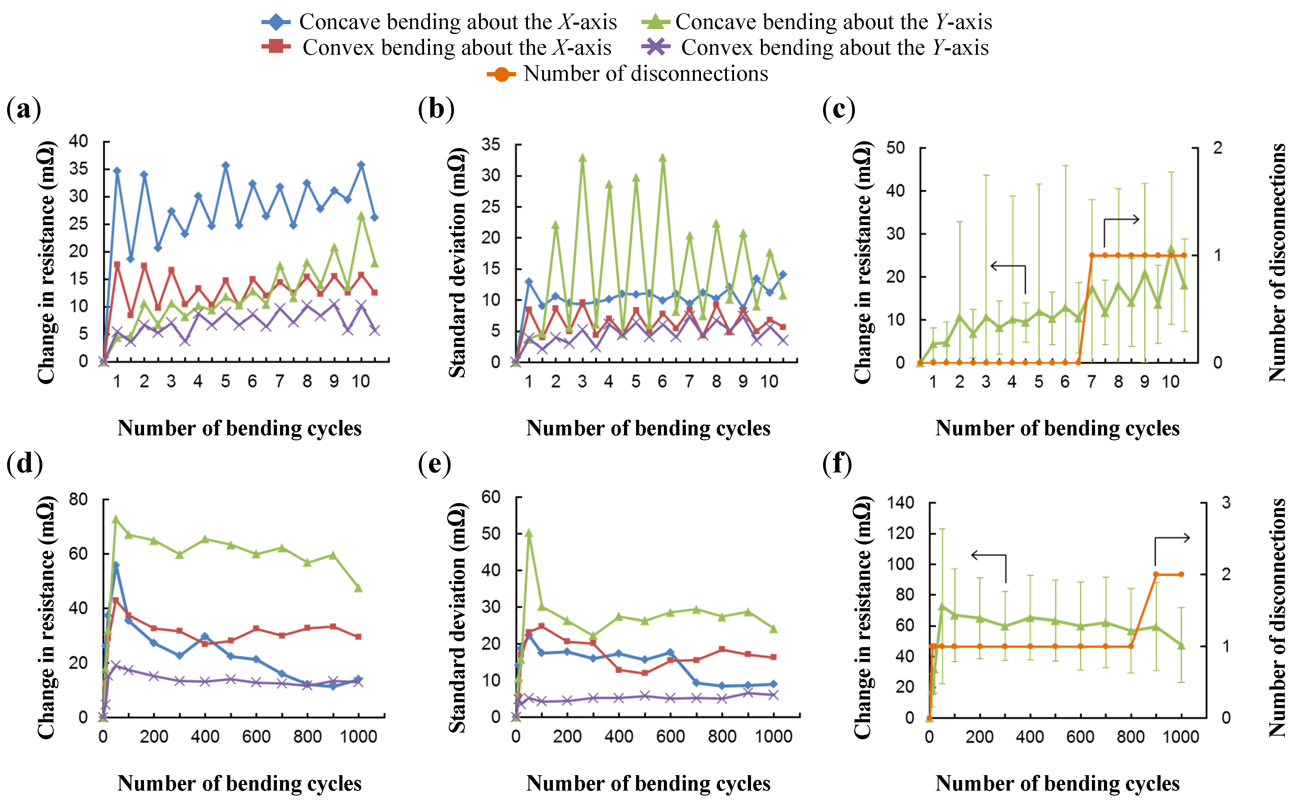
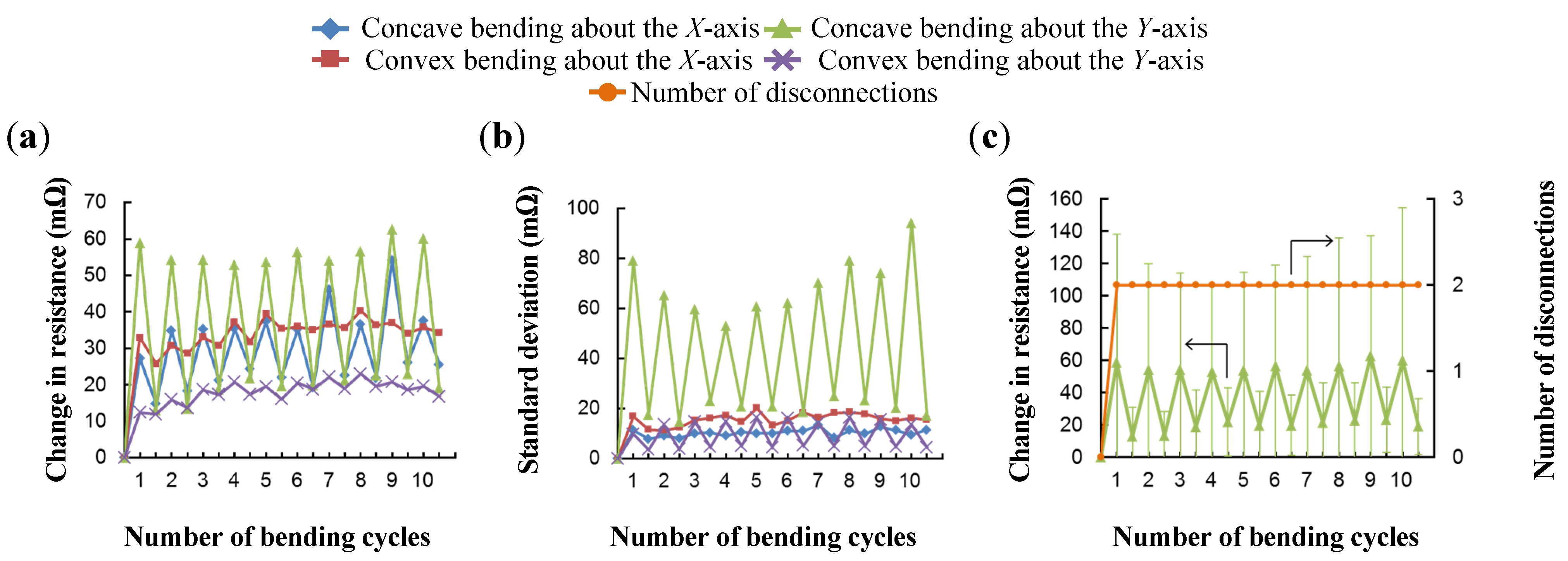
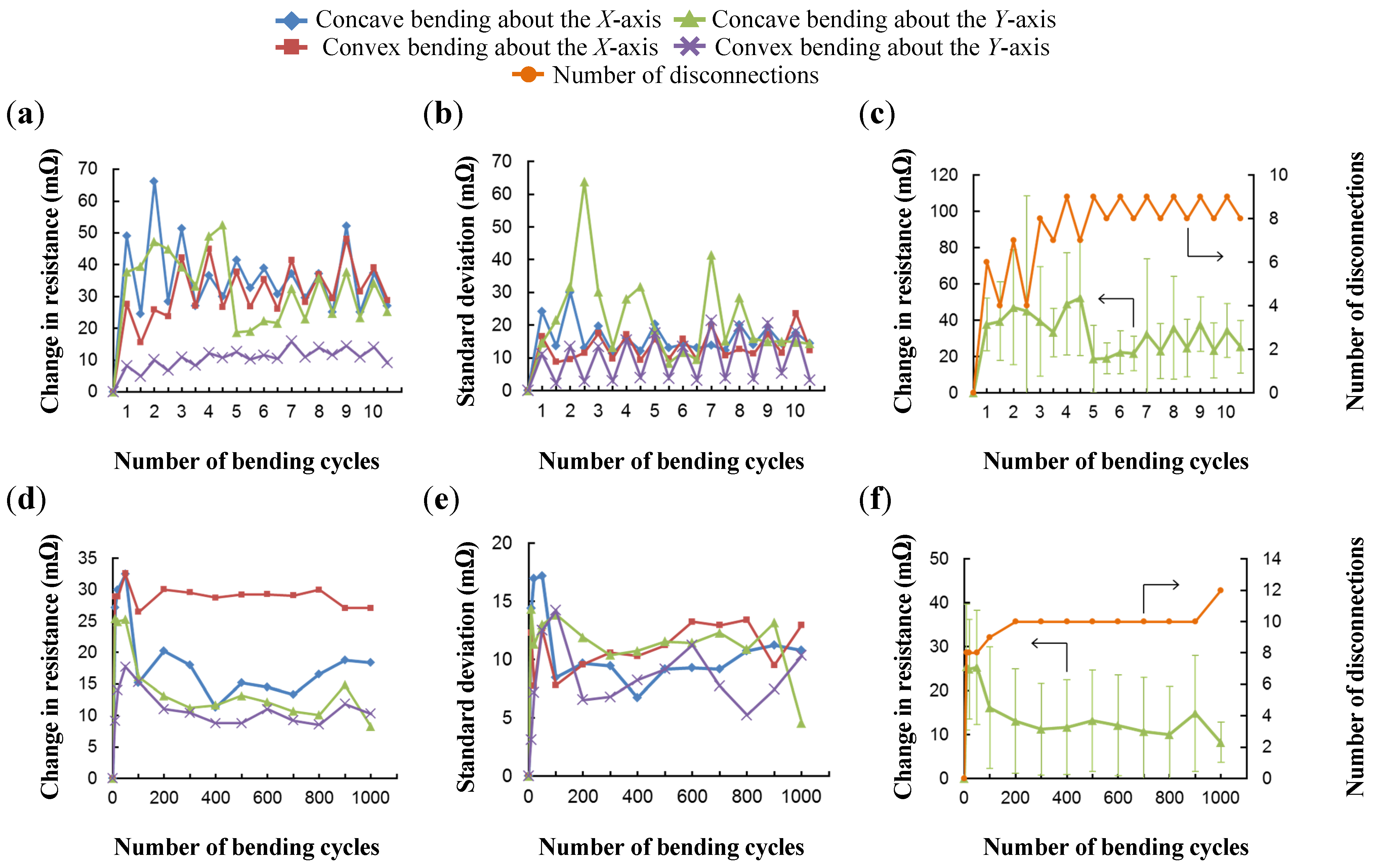
3. Results and Discussion

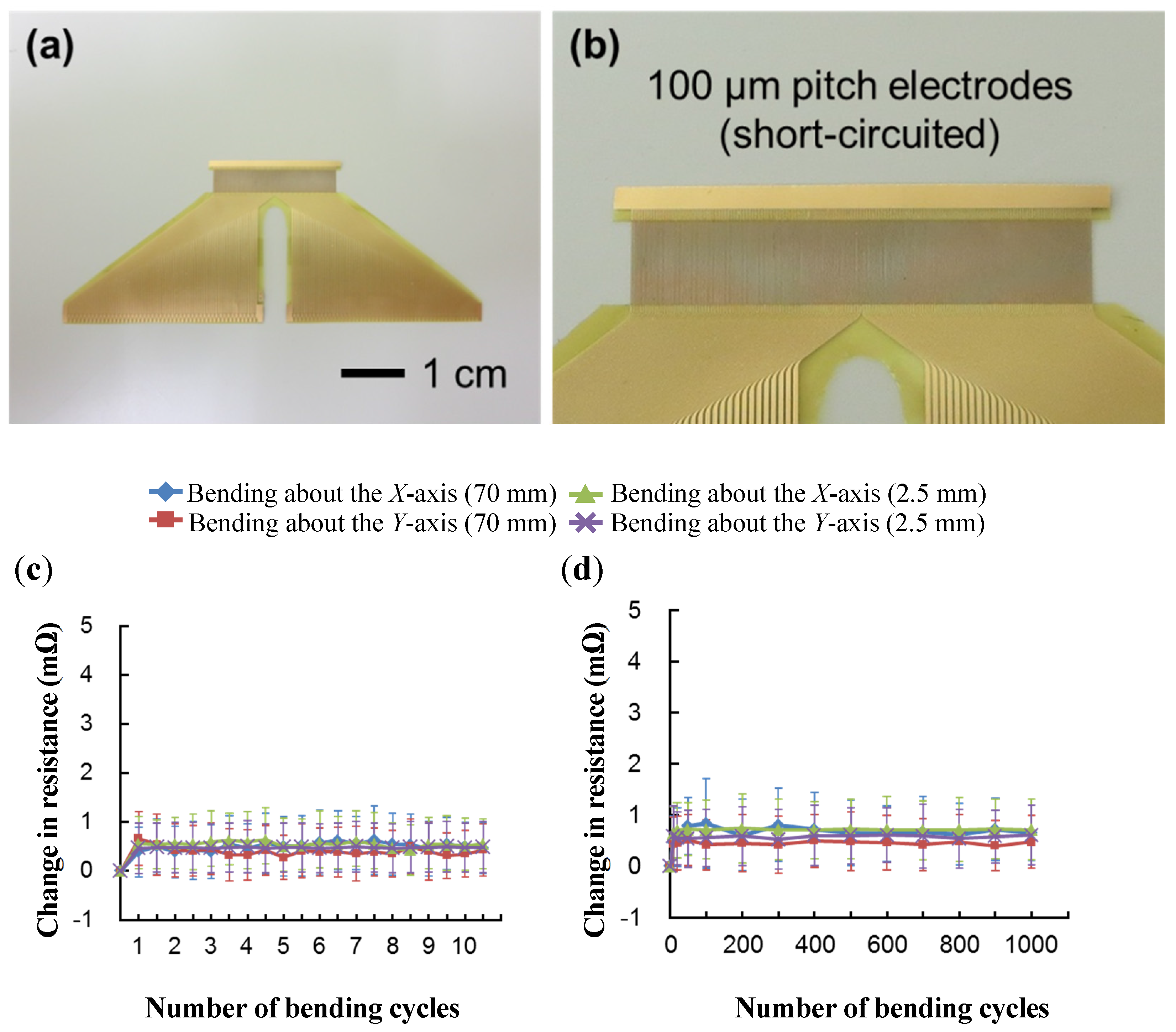
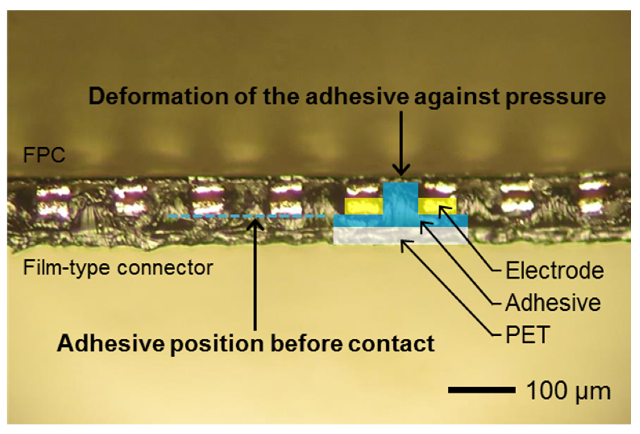
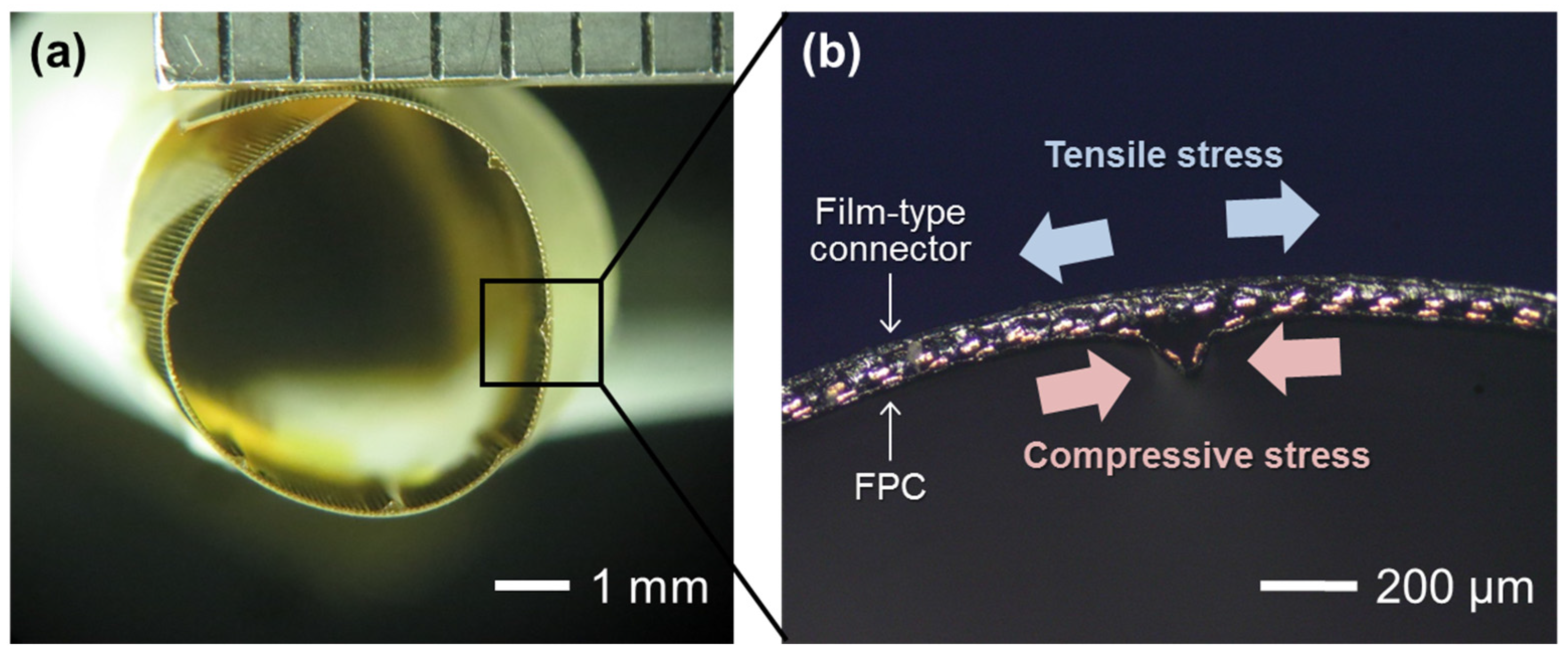
3.1. Characteristics of the Film-Type Connection
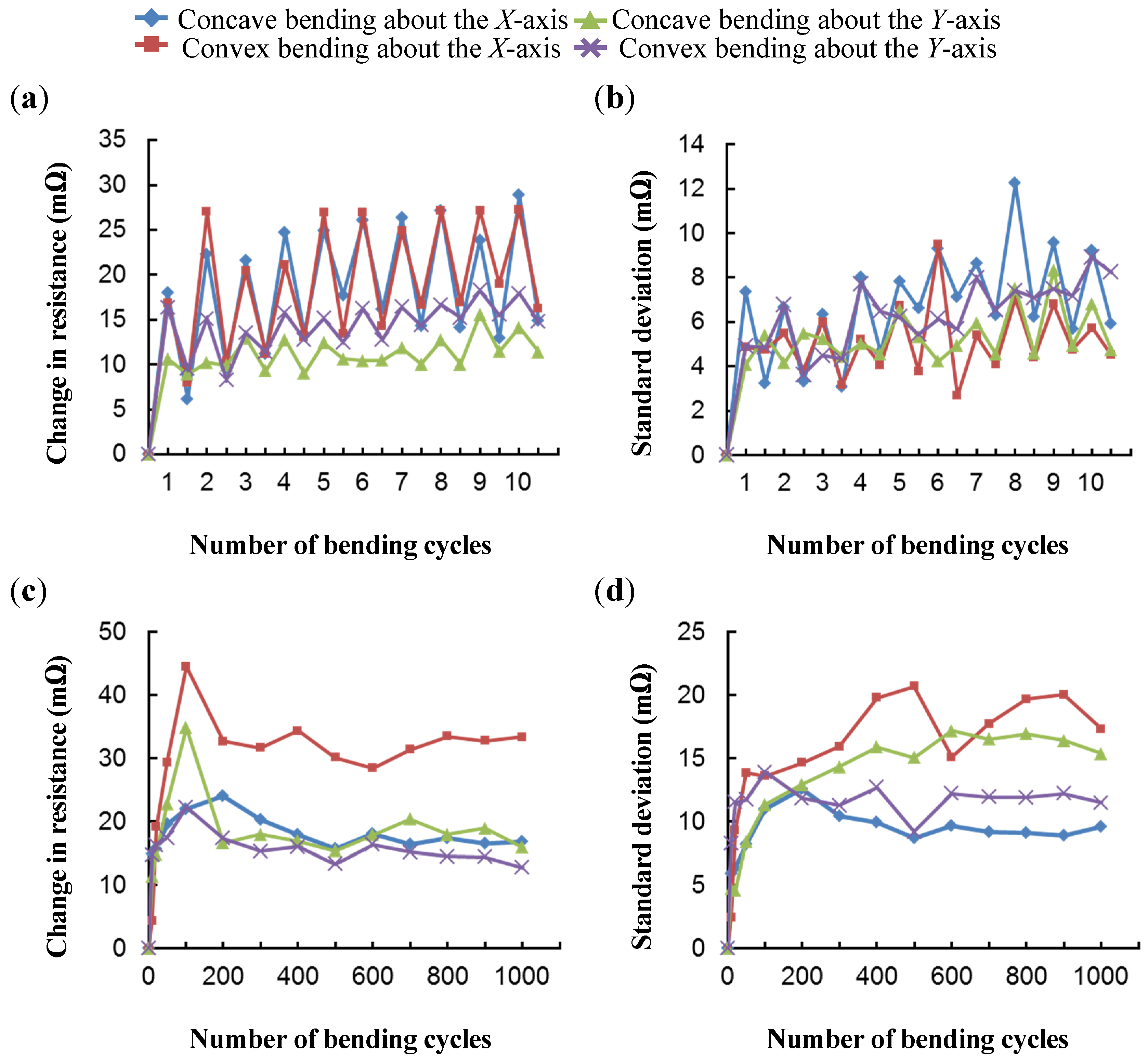
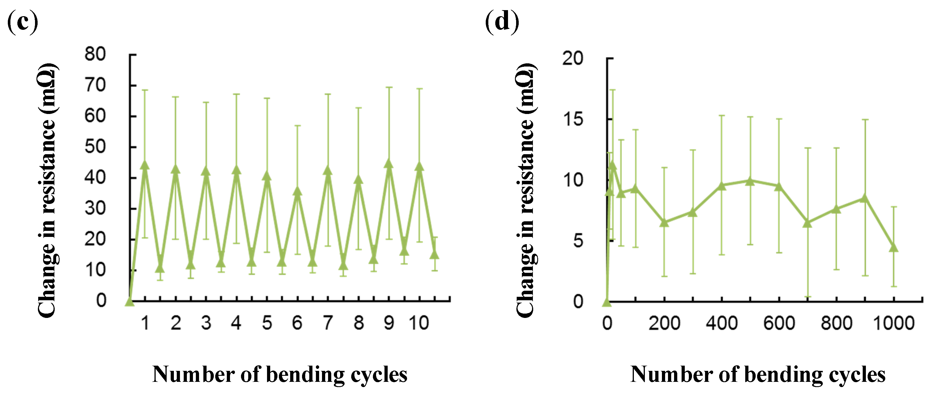
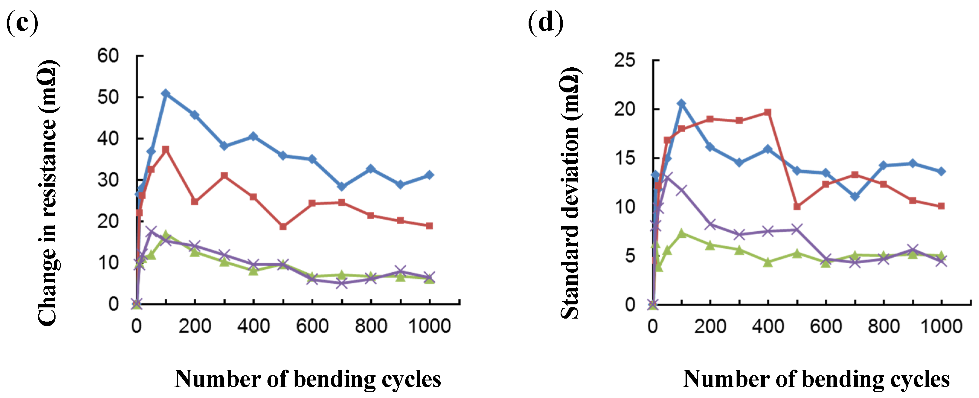
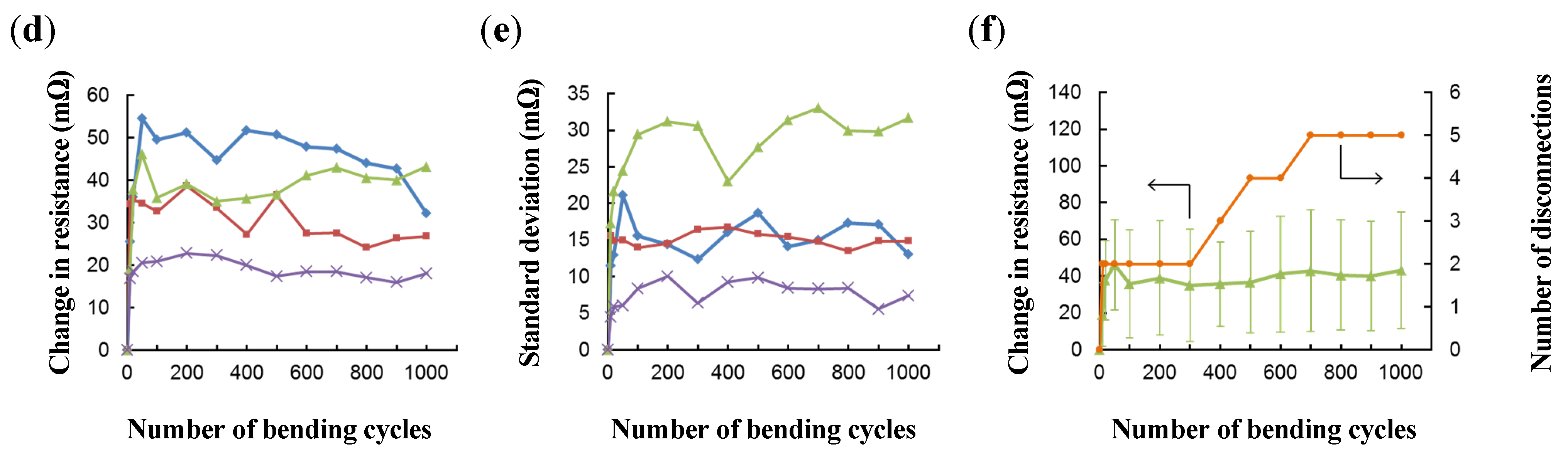
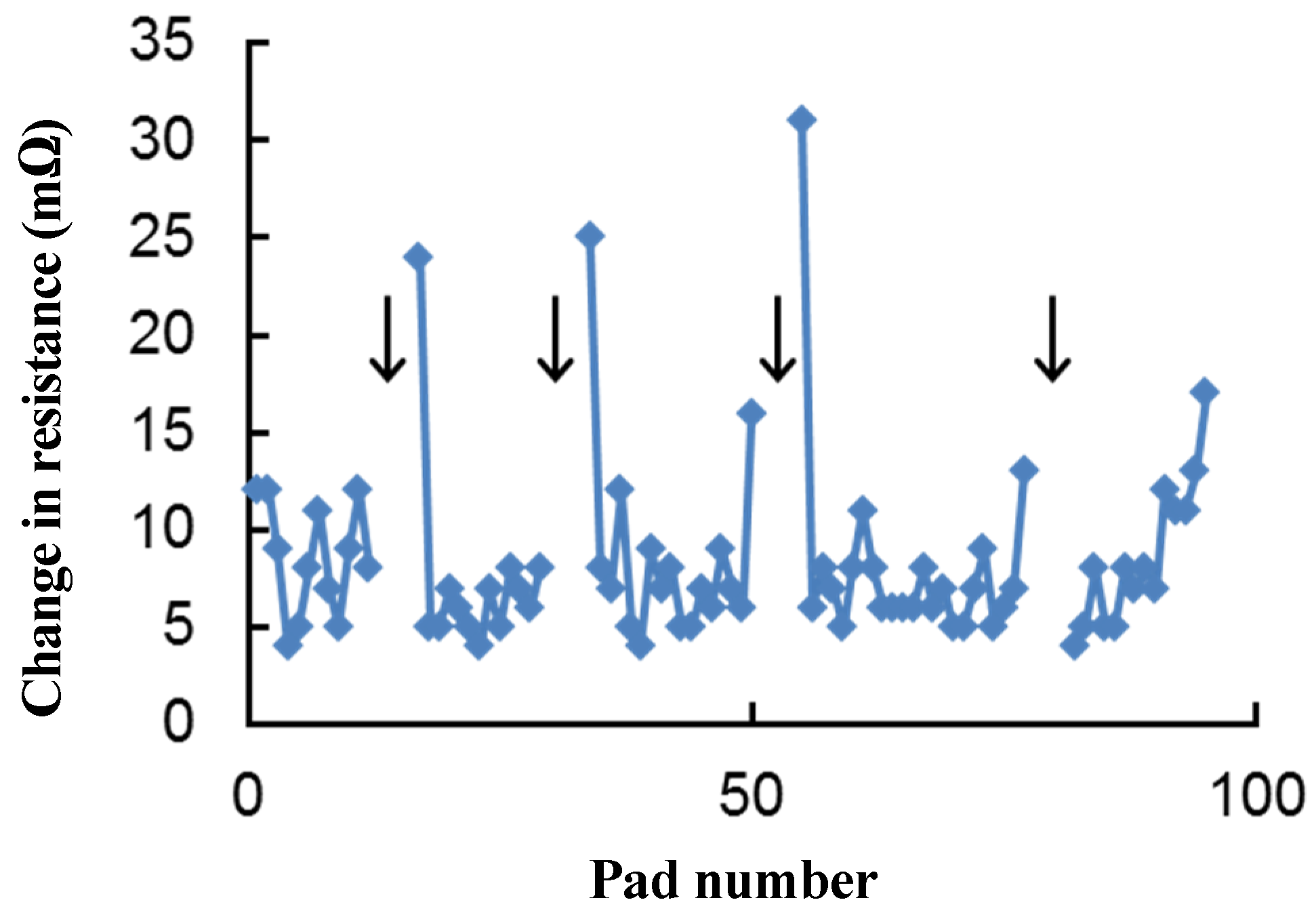
Figure 7 shows a typical connection process of a commercially available ACF with the FPC. When an ACF is used, conductive particles are sandwiched and deformed by the pressure applied between the electrodes, and the connections are established by the compressive force between the electrodes due to the shrinkage of the adhesive after curing. As previously described, the connection procedure of the proposed film-type connector is performed at room temperature, whereas the general ACF bonding process requires heating (Figure 2 and Figure 7). Although several technologies have been proposed to reduce the bonding temperature of ACFs, they require temperatures higher than 100 °C near the connector, even when using ultrasonic vibrations [43,44,45]. In addition, film-type connectors require a lower pressure than do ACFs (e.g., 1.5 MPa vs. 3 MPa). The modulus of elasticity of the adhesive that is used in the film-type connector can be as high as 30 MPa at 25 °C even after curing, which is more flexible than the GPa level of the moduli of elasticity of the thermosetting resins that are used in standard ACFs [46,47,48,49,50]. For these reasons, the film-type connector is considered to be superior to existing ACFs because of the moderate nature of the connection process, the minimal damage to the connecting objects, and the flexibility of the junction [42].
Figure 7. Connection process using ACFs.
Electronics 04 00827 g007
Figure 8 shows a cross-sectional image of the junction of the film-type connection. The adhesive is compressed to approximately 80% of its thickness by the pressure that is applied during the connection. Although the contact pressure is not measured experimentally, we can assume that the connection pressure between the electrodes results from the elastic restoring force of the adhesive. The experimental and mathematical investigations in this study indicate that the real contact area allows for electrical conductance because the two metals are in contact with each other over some of the apparent contact area [51,52,53,54,55,56]. Thus, the film-type connector forms a plate-to-plate contact between the electrode and the connecting unit, which ensures the maximum apparent and real contact areas. In addition, the film-type connector has a total thickness of less than 100 µm; thus, it can be connected without sacrificing the design of a flexible device.
Figure 8. Cross-sectional image of the junction.
Electronics 04 00827 g008
Figure 9 shows the measurement results for the film-type connection in the unbent condition using the four-point probe method. The arrow with the continuous line in the figure describes the flow of the electric current. The current flows from pad 1 to the adjacent pad 2 via the comb-like electrode of the FPC that is connected to the film-type connector. The results show that the length of the current flow is closely correlated to the wiring resistance and that there is no disconnection or failure of the connection. The results strongly suggest that the film-type connector was appropriately connected to the FPC.
Figure 9. Resistance of the film-type connection.
Electronics 04 00827 g009

3.2. Bending Tests

First, the change in resistance of the film-type connector whose electrodes were electrically shorted during bending tests was measured to investigate the change in wiring resistance. Figure 10a,b show the appearance of the electrically shorted film-type connector. Figure 10c,d show the results of the continuous and intermittent measurements at curvature radii of 70 and 2.5 mm. In Figure 10c, every measurement between the bent states indicates the resistance in the unbent state; resistance was measured while alternately moving the sample from the bent to the unbent state. In contrast, Figure 10d shows the change in resistance that was measured in the unbent state after different numbers of bending cycles. These results suggest that the maximum change in the wiring resistance is approximately 1.5 milliohms regardless of the curvature radius.
Figure 10. Investigation of the change in wiring resistance: (a,b) appearance of the electrically shorted film-type connector; (c) continuous measurements; and (d) intermittent measurements.
Electronics 04 00827 g010
Figure 11, Figure 12, Figure 13, Figure 14, Figure 15 and Figure 16 show the results of the bending test at each curvature radius. The results of the bending tests at curvature radii of 70, 50, and 25 mm (Figure 11, Figure 12 and Figure 13) showed that the connection using the film-type connector is relatively stable against mechanical deformation [42]; no disconnections were observed even after 1000 bending cycles. Although the change in resistance and the standard deviation of the continuous measurements generally increased as the number of bending cycles increased, the change in the resistance and the standard deviation of the unbent states were smaller than those of the previous bent states. The change in resistance and the standard deviation increased in a zigzag manner during repeated bending. In the intermittent measurements, the resistance decreased as the number of bending cycles increased, with maximum values between 100–200 cycles. The change in resistance during bending was mainly dominated by the change in the contact resistance because the change in the wiring resistance was sufficiently low as to be negligible (Figure 10). In addition, the junctions tended to be more stable during bending about the Y-axis than during bending about the X-axis.
Figure 11. Change in resistance during the bending test for a curvature radius of 70 mm: (a,b) continuous measurements and (c,d) intermittent measurements.
Electronics 04 00827 g011
Figure 12. Change in resistance during the bending test for a curvature radius of 50 mm: (a,b) continuous measurements and (c,d) intermittent measurements.
Electronics 04 00827 g012aElectronics 04 00827 g012b
Figure 13. Change in resistance during the bending test for a curvature radius of 25 mm: (a,b) continuous measurements and (c,d) intermittent measurements.
Electronics 04 00827 g013
Figure 14, Figure 15 and Figure 16 show the results of the bending tests at curvature radii of 10, 5, and 2.5 mm. In the continuous measurements, the general trend was similar to the case of the larger curvature radii except for the occurrence of disconnections. In the case of concave bending about the Y-axis, some disconnections were generated when the radius of curvature was less than 10 mm. The number of disconnections increased as the curvature radius decreased. In particular, in the case of concave bending about the Y-axis with a curvature radius of 2.5 mm, the number of disconnections increased in a zigzag manner (Figure 16c). These results suggest that the delamination of the adhesive that is bonded to the FPC substrate gradually increases with the number of mechanical deformation cycles. The general trend of the intermittent measurements was also similar to that of the larger curvature radii except for the occurrence of disconnections. Plastic deformation of the connection was observed during the bending test. These results indicate that plastic deformation of the connection in the bending direction suppresses the deformation of the adhesive. Therefore, the original elastic restoring force of the adhesive is likely induced (Figure 17). From a long-term perspective, the disconnections that are caused by the delamination of the adhesive are irreversible.
Figure 14. Change in resistance during the bending test for a curvature radius of 10 mm: (ac) continuous measurements; (df) intermittent measurements; and (c,f) concave bending about the Y-axis.
Electronics 04 00827 g014
Figure 15. Change in resistance during the bending test for a curvature radius of 5 mm: (ac) continuous measurements; (df) intermittent measurements; and (c,f) concave bending about the Y-axis.
Electronics 04 00827 g015aElectronics 04 00827 g015b
Figure 16. Change in resistance during the bending test for a curvature radius of 2.5 mm: (ac) continuous measurements; (df) intermittent measurements; and (c,f) concave bending about the Y-axis.
Electronics 04 00827 g016
Figure 18 shows a cross-sectional image of the junction during concave bending about the Y-axis at a curvature radius of 2.5 mm. The disconnections and slippage of the electrode are observed to follow a cyclic pattern. These results suggest that the compressive stress that is produced in the FPC is caused by the bending deformation [57]. Conversely, during convex bending about the Y-axis, the FPC is subjected to a tensile stress that maintains the connection. This behavior occurs because the thicker substrate has a high resistance to compressive stress; the PET substrate is 25 µm thick, whereas the PI film is 7.5 µm thick. The PI film that is used in the FPC is more easily deformed than the PET substrate; therefore, no disconnections occurred even at a curvature radius of 2.5 mm. However, despite the compressive stress that is generated during concave bending about the X-axis, no disconnections occurred due to the deformation. The direction of the compressive stress is apparently correlated with the direction of the electrode. For the compressive stress that is parallel to the long side of the electrode (i.e., bending about the X-axis), the adhesive force that resists the compressive stress is maximized in the adhesion domain because the adhesive is pushed out from between the film-type connector electrode. Conversely, for the compressive stress that is perpendicular to the long side of the electrode (i.e., bending about the Y-axis), the adhesive force that resists the compressive stress decreases due to the presence of the electrode between the adhesive. Every cross-section of the junction within the film-type connector contains electrodes, and these electrodes only lightly touch the FPC electrodes and do not increase the adhesive force. The plate-to-plate contact contributes to securing the contact area even in the case of electrode slippage.
Figure 17. Photograph of the plastic deformation of the connection during the bending test.
Electronics 04 00827 g017
Figure 18. Cross-sectional image of the junction of the film-type connection: (a) complete image of the junction and (b) enlarged image of a disconnection.
Electronics 04 00827 g018
In summary, bending about the Y-axis causes regional deformation, whereas bending about the X-axis causes overall deformation. When bending occurs about the Y-axis, the change in resistance is relatively stable because the long side of the electrodes remains unbent (electrode slippage occurs to reduce the distortion), but the amount of electrode slippage during bending at low curvature radii is greater than that at larger curvature radii because of the flexibility of the adhesive and/or the separation of the adhesive that is caused by the local compressive stress concentration; as a result, disconnections can occur. Figure 19 shows the change in resistance of the film-type connection in the unbent condition after 1000 bending cycles for a curvature radius of 2.5 mm. The arrows in the figure show the locations where the disconnections occurred. The change in resistance of most of the connections remains relatively stable except in the compartment around the disconnection. In contrast, during bending about the X-axis, the stress that is related to the separation of the adhesive from the FPC substrate is high (the long side of the electrodes is bent directly, and the change of the connection state between the FPC electrode and the connecting electrode causes the change in the contact resistance to be large), but the electrode slippage does not influence the disconnection because if electrode slippage occurs, it occurs in the same direction as the long side of the electrodes.
Figure 19. Change in resistance of the film-type connection in the unbent condition after 1000 bending cycles for a curvature radius of 2.5 mm.
Electronics 04 00827 g019
It is desirable that no disconnections occur. The 192 electrodes of the FPC were periodically thinned out to 182 electrodes to avoid the cyclic pattern of disconnections (Figure 20a), and a concave bending test about the Y-axis at a curvature radius of 2.5 mm was performed. Figure 20b shows a cross-sectional image of the junction. The arrows in the figure show the locations where the electrodes were removed. The results of the bending tests suggest that the removal of electrodes is effective in preventing disconnections (Figure 16c vs. Figure 20c and Figure 16f vs. Figure 20d). This is because the thinning out of the electrodes allows for the movement of electrodes to prevent local compressive stress concentrations.
Figure 20. Bending test with the FPC in which electrodes were removed: (a) photograph of the thinned out FPC (182 electrodes); (b) cross-sectional image of the junction; (c) continuous measurements; and (d) intermittent measurements.
Electronics 04 00827 g020aElectronics 04 00827 g020b

4. Conclusions

This study described the fabrication process of a film-type connection with a UV-curable adhesive and the electrical reliability of the connection during bending. The proposed film-type connector, which is less than 0.1 mm thick, was composed of a base material, such as PI film, an adhesive layer that deforms elastically with pressure, and electrodes that are arranged on the adhesive layer. Bending tests of the junction were performed at curvature radii of 70, 50, 25, 10, 5, and 2.5 mm to examine the possible applications of this junction in flexible electronics. The results show that the plate-to-plate contact of the film-type connection was robust and effective during the deformation of the junction. We also demonstrated that disconnections of the junction are only generated by concave bending along the Y-axis at curvature radii of 10, 5, and 2.5 mm due to compressive stresses. Potential uses of the proposed connection method were identified based on the results of the investigation, and applications of such a connection in areas such as future flexible electronics were suggested. Future studies in this field should focus on the development of a novel connection system that exhibits desirable electrical properties under stretching conditions.

Author Contributions

R.M. designed the research methods that were used in this study. All the authors contributed equally to the data analysis, the interpretation of the results and the preparation of the manuscript. All the authors read and approved the final manuscript.

Conflicts of Interest

The authors declare no conflicts of interest.

References

  1. Fjelstad, J. Flexible Circuit Technology, 4th ed.; BR Publishing: Seaside, OR, USA, 2011. [Google Scholar]
  2. Leong, W.C.; Abdullah, M.Z.; Khor, C.Y. Application of flexible printed circuit board (FPCB) in personal computer motherboards: Focusing on mechanical performance. Microelectron. Reliab. 2012, 52, 744–756. [Google Scholar] [CrossRef]
  3. Constable, J.H.; Kache, T.; Teichmann, H.; Mühle, S.; Gaynes, M.A. Continuous electrical resistance monitoring, pull strength, and fatigue life of isotropically conductive adhesive joints. IEEE Trans. Compon. Packag. Technol. 1999, 22, 191–199. [Google Scholar] [CrossRef]
  4. Yim, M.J.; Paik, K.W. Recent advances on anisotropic conductive adhesives (ACAs) for flat panel displays and semiconductor packaging applications. Int. J. Adhes. Adhes. 2006, 26, 304–313. [Google Scholar] [CrossRef]
  5. Xie, B.; Shi, X.Q.; Ding, H. Understanding of delamination mechanism of anisotropic conductive film (ACF) bonding in thin liquid crystal display (LCD) module. IEEE Trans. Compon. Packag. Technol. 2007, 30, 509–516. [Google Scholar] [CrossRef]
  6. Sheng, X.; Jia, L.; Xiong, Z.; Wang, Z.; Ding, H. ACF-COG interconnection conductivity inspection system using conductive area. Microelectron. Reliab. 2013, 53, 622–628. [Google Scholar] [CrossRef]
  7. Nathan, A.; Ahnood, A.; Cole, M.T.; Lee, S.; Suzuki, Y.; Hiralal, P.; Bonaccorso, F.; Hasan, T.; Garcia-Gancedo, L.; Dyadyusha, A.; et al. Flexible electronics: The next ubiquitous platform. Proc. IEEE 2012, 100, 1486–1517. [Google Scholar] [CrossRef]
  8. Ko, H.; Kapadia, R.; Takei, K.; Takahashi, T.; Zhang, X.; Javey, A. Multifunctional, flexible electronic systems based on engineered nanostructured materials. Nanotechnology 2012, 23, 344001. [Google Scholar] [CrossRef] [PubMed]
  9. Zhou, L.; Wanga, A.; Wu, S.C.; Sun, J.; Park, S.; Jackson, T.N. All-organic active matrix flexible display. Appl. Phys. Lett. 2006, 88, 083502. [Google Scholar] [CrossRef]
  10. Choi, M.C.; Kim, Y.; Ha, C.S. Polymers for flexible displays: From material selection to device applications. Prog. Polym. Sci. 2008, 33, 581–630. [Google Scholar] [CrossRef]
  11. Delmdahl, R.; Fricke, M.; Fechner, B. Laser lift-off systems for flexible-display production. J. Inf. Disp. 2014, 15, 1–4. [Google Scholar] [CrossRef]
  12. Li, C.; Han, J.; Ahn, C.H. Flexible biosensors on spirally rolled micro tube for cardiovascular in vivo monitoring. Biosens. Bioelectron. 2007, 22, 1988–1993. [Google Scholar] [CrossRef] [PubMed]
  13. Kwon, O.S.; Park, E.; Kweon, O.Y.; Park, S.J.; Jang, J. Novel flexible chemical gas sensor based on poly(3,4-ethylenedioxythiophene) nanotube membrane. Talanta 2010, 82, 1338–1343. [Google Scholar] [CrossRef] [PubMed]
  14. Segev-Bar, M.; Haick, H. Flexible sensors based on nanoparticles. ACS Nano 2013, 7, 8366–8378. [Google Scholar] [CrossRef] [PubMed]
  15. Wang, J.Z.; Chou, S.L.; Liu, H.; Wang, G.X.; Zhong, C.; Chew, S.Y.; Liu, H.K. Highly flexible and bendable free-standing thin film polymer for battery application. Mater. Lett. 2009, 63, 2352–2354. [Google Scholar] [CrossRef]
  16. Pushparaj, V.L.; Shaijumon, M.M.; Kumar, A.; Murugesan, S.; Ci, L.; Vajtai, R.; Linhardt, R.J.; Nalamasu, O.; Ajayan, P.M. Flexible energy storage devices based on nanocomposite paper. Proc. Natl. Acad. Sci. USA 2007, 104, 13574–13577. [Google Scholar] [CrossRef] [PubMed]
  17. Zhou, G.; Li, F.; Cheng, H.M. Progress in flexible lithium batteries and future prospects. Energy Environ. Sci. 2014, 7, 1307–1338. [Google Scholar] [CrossRef]
  18. Pagliaro, M.; Ciriminna, R.; Palmisano, G. Flexible solar cells. ChemSusChem 2008, 1, 880–891. [Google Scholar] [CrossRef] [PubMed]
  19. Yang, L.; Zhang, T.; Zhou, H.; Price, S.C.; Wiley, B.J.; You, W. Solution-processed flexible polymer solar cells with silver nanowire electrodes. ACS Appl. Mater. Interfaces 2011, 3, 4075–4084. [Google Scholar] [CrossRef] [PubMed]
  20. Brown, T.M.; de Rossi, F.; di Giacomo, F.; Mincuzzi, G.; Zardetto, V.; Reale, A.; di Carlo, A. Progress in flexible dye solar cell materials, processes and devices. J. Mater. Chem. A 2014, 2, 10788–10817. [Google Scholar] [CrossRef]
  21. Ji, Y.; Lee, S.; Cho, B.; Song, S.; Lee, T. Flexible organic memory devices with multilayer graphene electrodes. ACS Nano 2011, 5, 5995–6000. [Google Scholar] [CrossRef] [PubMed]
  22. Lai, Y.C.; Wang, Y.X.; Huang, Y.C.; Lin, T.Y.; Hsieh, Y.P.; Yang, Y.J.; Chen, Y.F. Rewritable, moldable, and flexible sticker-type organic memory on arbitrary substrates. Adv. Funct. Mater. 2014, 24, 1430–1438. [Google Scholar] [CrossRef]
  23. Han, S.T.; Zhou, Y.; Roy, V.A.L. Towards the development of flexible non-volatile memories. Adv. Mater. 2013, 25, 5425–5449. [Google Scholar] [CrossRef] [PubMed]
  24. Kris, M.; Soeren, S.; Peter, V.; Monique, B.; van Aerle, N.A.J.M.; Gerwin, H.G.; Jan, G.; Wim, D.; Paul, H. Plastic circuits and tags for 13.56 MHz radio-frequency communication. Solid-State Electron. 2009, 53, 1220–1226. [Google Scholar]
  25. Babar, A.A.; Bjorninen, T.; Bhagavati, V.A.; Sydänheimo, L.; Kallio, P.; Ukkonen, L. Small and flexible metal mountable passive UHF RFID tag on high-dielectric polymer-ceramic composite substrate. IEEE Antennas Wirel. Propag. Lett. 2012, 11, 1319–1322. [Google Scholar] [CrossRef]
  26. Martínez-Olmos, A.; Fernández-Salmerón, J.; Lopez-Ruiz, N.; Torres, A.R.; Capitan-Vallvey, L.F.; Palma, A.J. Screen printed flexible radiofrequency identification tag for oxygen monitoring. Anal. Chem. 2013, 85, 11098–11105. [Google Scholar] [CrossRef] [PubMed]
  27. Ruffini, G.; Dunne, S.; Fuentemilla, L.; Grau, C.; Farrés, E.; Marco-Pallarés, J.; Watts, P.C.P.; Silva, S.R.P. First human trials of a dry electrophysiology sensor using a carbon nanotube array interface. Sens. Actuators A 2008, 144, 275–279. [Google Scholar] [CrossRef]
  28. Kim, D.-H.; Lu, N.; Ma, R.; Kim, Y.-S.; Kim, R.-H.; Wang, S.; Wu, J.; Won, S.M.; Tao, H.; Islam, A.; et al. Epidermal electronics. Science 2011, 333, 838–843. [Google Scholar] [CrossRef] [PubMed]
  29. Pang, C.; Lee, C.; Suh, K.Y. Recent advances in flexible sensors for wearable and implantable devices. J. Appl. Polym. Sci. 2013, 130, 1429–1441. [Google Scholar] [CrossRef]
  30. Forrest, S.R. The path to ubiquitous and low-cost organic electronics appliances on plastic. Nature 2004, 428, 911–918. [Google Scholar] [CrossRef] [PubMed]
  31. Søndergaard, R.R.; Hösel, M.; Krebs, F.C. Roll-to-roll fabrication of large area functional organic materials. J. Polym. Sci. Polym. Phys. 2013, 51, 16–34. [Google Scholar] [CrossRef]
  32. Alzoubi, K.; Hamasha, M.M.; Lu, S.; Sammakia, B. Bending fatigue study of sputtered ITO on flexible substrate. J. Disp. Technol. 2011, 7, 593–600. [Google Scholar] [CrossRef]
  33. Hamasha, M.M.; Alzoubi, K.; Lu, S.; Desu, S.B. Durability study on sputtered indium tin oxide thin film on poly ethylene terephthalate substrate. Thin Solid Films 2011, 519, 6033–6038. [Google Scholar] [CrossRef]
  34. Peng, C.-Y.; Dhakal, T.P.; Garner, S.M.; Cimo, P.; Lu, S.; Westgate, C.R. Strained growth of aluminum-doped zinc oxide on flexible glass substrate and degradation studies under cyclic bending conditions. IEEE Trans. Device Mater. Reliab. 2014, 14, 121–126. [Google Scholar] [CrossRef]
  35. Hamasha, M.M.; Alzoubi, K.; Switzer, J.C.; Lu, S.; Poliks, M.D.; Westgate, C.R. Reliability of sputtered aluminum thin film on flexible substrate under high cyclic bending fatigue condition. IEEE Trans. Compon. Packag. Manuf. Technol. 2012, 2, 2007–2016. [Google Scholar] [CrossRef]
  36. Peng, C.Y.; Hamasha, M.M.; VanHart, D.; Lu, S.; Westgate, C.R. Electrical and optical degradation studies on AZO thin films under cyclic bending conditions. IEEE Trans. Device Mater. Reliab. 2013, 31, 236–244. [Google Scholar] [CrossRef]
  37. Cho, C.K.; Hwang, W.J.; Eun, K.; Choa, S.H.; Na, S.I.; Kim, H.K. Mechanical flexibility of transparent PEDOT:PSS electrodes prepared by gravure printing for flexible organic solar cells. Sol. Energy Mater. Sol. Cell 2011, 95, 3269–3275. [Google Scholar] [CrossRef]
  38. Lee, H.M.; Lee, H.B.; Jung, D.S.; Yun, J.Y.; Ko, S.H.; Park, S.B. Solution processed aluminum paper for flexible electronics. Langmuir 2012, 28, 13127–13135. [Google Scholar] [CrossRef] [PubMed]
  39. Koo, M.; Park, K.I.; Lee, S.H.; Suh, M.; Jeon, D.Y.; Choi, J.W.; Kang, K.; Lee, K.J. Bendable inorganic thin-film battery for fully flexible electronic systems. Nano Lett. 2012, 12, 4810–4816. [Google Scholar] [CrossRef] [PubMed]
  40. Trung, T.Q.; Tien, N.T.; Kim, D.; Jang, M.; Yoon, O.J.; Lee, N.E. A flexible reduced graphene oxide field-effect transistor for ultrasensitive strain sensing. Adv. Funct. Mater. 2014, 24, 117–124. [Google Scholar] [CrossRef]
  41. Yeo, J.; Kim, G.; Hong, S.; Kim, M.S.; Kim, D.; Lee, J.; Lee, H.B.; Kwon, J.; Suh, Y.D.; Kang, H.W.; et al. Flexible supercapacitor fabrication by room temperature rapid laser processing of roll-to-roll printed metal nanoparticle ink for wearable electronics application. J. Power Sources 2014, 246, 562–568. [Google Scholar] [CrossRef]
  42. Mitsui, R.; Takahashi, S.; Nakajima, S.; Nomura, K.; Ushijima, H. Film-type connection system toward flexible electronics. Jpn. J. Appl. Phys. 2014, 53, 05HB04. [Google Scholar] [CrossRef]
  43. Choi, K.S.; Lee, H.; Bae, H.C.; Eom, Y.S.; Lee, J.H. Interconnection technology based on InSn solder for flexible display applications. ETRI J. 2015, 37, 387–394. [Google Scholar] [CrossRef]
  44. Kim, J.M.; Song, Y.; Cho, M.; Lee, S.H.; Shin, Y.E. Characteristics of thermosonic anisotropic conductive adhesives (ACFs) flip-chip bonding. Mater. Trans. 2010, 51, 1790–1795. [Google Scholar] [CrossRef]
  45. Lee, K.; Kim, H.J.; Kim, I.; Paik, K.W. Ultrasonic anisotropic conductive films (ACFs) bonding of flexible substrates on organic rigid boards at room temperature. In Proceedings of the 57th IEEE Electronic Components and Technology Conference (ECTC’07), Reno, NV, USA, 29 May–1 June 2007; pp. 480–486.
  46. Hwang, J.W.; Yim, M.J.; Paik, K.W. Effects of thermoplastic resin content of anisotropic conductive films on the pressure cooker test reliability of anisotropic conductive film flip-chip assembly. J. Electron. Mater. 2005, 34, 1455–1461. [Google Scholar] [CrossRef]
  47. Rizvi, M.J.; Chan, Y.C.; Bailey, C.; Lu, H. Study of anisotropic conductive adhesive joint behavior under 3-point bending. Microelectron. Reliab. 2005, 45, 589–596. [Google Scholar] [CrossRef]
  48. Jang, K.W.; Paik, K.W. Effects of heating rate on material properties of anisotropic conductive film (ACF) and thermal cycling reliability of ACF flip chip assembly. IEEE Trans. Compon. Packag. Technol. 2009, 32, 339–346. [Google Scholar] [CrossRef]
  49. Ma, J.; Gao, H.; Gao, L.; Chen, X. Uniaxial ratcheting behavior of anisotropic conductive adhesive film at elevated temperature. Polym. Test. 2011, 30, 571–577. [Google Scholar] [CrossRef]
  50. Leu, J.; Chang, C.C.; Chen, A.; Lin, M.H.; Huang, K.F. Effects of localized warpage and stress on chip-on-glass packaging: Induced light-leakage phenomenon in mid-sized TFT-LCD. J. Soc. Inf. Disp. 2012, 20, 28–36. [Google Scholar] [CrossRef]
  51. Braunović, M.; Konchits, V.V.; Myshkin, N.K. Electrical Contacts: Fundamentals, Applications and Technology; CRC Press: Boca Raton, FL, USA, 2006. [Google Scholar]
  52. Sawada, S.; Tamai, T.; Hattori, Y.; Iida, K. Numerical analyses for contact resistance due to constriction effect of current flowing through multi-spot construction. IEICE Trans. Electron. 2010, E93-C, 905–911. [Google Scholar] [CrossRef]
  53. Leidner, M.; Schmidt, H.; Myers, M.; Schlaak, H.F. A new simulation approach to characterizing the mechanical and electrical qualities of a connector contact. Eur. Phys. J. Appl. Phys. 2010, 49, 22909. [Google Scholar] [CrossRef]
  54. Pennec, F.; Peyrou, D.; Leray, D.; Pons, P.; Plana, R.; Courtade, F. Impact of the surface roughness description on the electrical contact resistance of ohmic switches under low actuation forces. IEEE Trans. Compon. Packag. Manuf. Technol. 2012, 2, 85–94. [Google Scholar] [CrossRef]
  55. Duan, K.; Zhu, F.; Li, Y.; Tang, K.; Liu, S.; Chen, Y. Contact resistance investigation of electrical connector with different shrink range. In Proceedings of the 15th International Conference on Electronic Packaging Technology (ICEPT 2014), Chengdu, China, 12–15 August 2014; pp. 1146–1149.
  56. Fukuyama, Y.; Sakamoto, N.; Kaneko, N.; Kondo, T.; Onuma, M. Constriction resistance of physical simulated electrical contacts with nanofabrication. In Proceedings of the IEEE 60th Holm Conference on Electrical Contacts (Holm 2014), New Orleans, LA, USA, 12–15 October 2014; pp. 216–220.
  57. Lewis, J. Material challenge for flexible organic devices. Mater. Today 2006, 9, 38–45. [Google Scholar] [CrossRef]

