Article

Organic Optical Sensor Based on Monolithic Integration of Organic Electronic Devices

Department of Physics, Institute of Advanced Materials, and Institute of Research and Continuing Education (Shenzhen), Hong Kong Baptist University, Kowloon Tong, NT, Hong Kong, China
*
Author to whom correspondence should be addressed.
Electronics 2015, 4(3), 623-632; https://doi.org/10.3390/electronics4030623
Submission received: 17 July 2015 / Revised: 5 September 2015 / Accepted: 10 September 2015 / Published: 17 September 2015
(This article belongs to the Special Issue Recent Advances in Organic Bioelectronics and Sensors)

Abstract

:
A novel organic optical sensor that integrates a front organic light-emitting diode (OLED) and an organic photodiode (OPD) is demonstrated. The stripe-shaped cathode is used in the OLED components to create light signals, while the space between the stripe-shaped cathodes serves as the detection window for integrated OPD units. A MoO3 (5 nm)/Ag (15 nm) bi-layer inter-electrode is interposed between the vertically stacked OLED and OPD units, serving simultaneously as the cathode for the front OLED and an anode for the upper OPD units in the sensor. In the integrated sensor, the emission of the OLED units is confined by the area of the opaque stripe-shaped cathodes, optimized to maximize the reflected light passing through the window space for detection by the OPD components. This can ensure high OLED emission output, increasing the signal/noise ratio. The design and fabrication flexibility of an integrated OLED/OPD device also has low cost benefits, and is light weight and ultra-thin, making it possible for application in wearable units, finger print identification, image sensors, smart light sources, and compact information systems.

Graphical Abstract

1. Introduction

Organic electronic devices have been developing rapidly and significant progress has been made in organic light emitting diode (OLED) displays, white OLED lighting, organic transistors, organic photodetectors (OPDs), and organic solar cells [1,2,3,4,5]. Compared to those devices based on inorganic semiconductor materials, which still play a major role in the optoelectronic market, the emerging organic electronic devices offer additional advantages such as large area, flexibility, and solution-based fabrication processes at low costs. Thin film organic optoelectronic devices offer an attractive option for achieving flexible organic electronics. Organic semiconducting materials as the active components in the devices have many advantages, e.g., thin, lightweight, large area, cost effectiveness, chemical tenability, and mechanical flexibility. A variety of organic optoelectronic systems are being explored for application in organic photonics in communication [6], all-polymeric optocouplers [7,8,9], chemical sensing [10,11], biosensing [12], refractometers [13], memory [14], and optical integrated systems [15,16].
The multilayer organic optoelectronic devices such as multiphoton emission devices [17,18], tandem organic solar cells [19], and OPDs with external quantum efficiencies up to 75% across visible light and bandwidths approaching 450 MHz have been reported [20]. A typical organic sensor consists of an OPD integrated with an OLED [21]. The integration of OPD with OLED in a stacked geometry results in better light coupling from OLED to OPD compared with that between discrete devices [22]. The integrated organic optical bi-functional matrix arrays [23] and bi-stable optical switches [24] have been demonstrated. An integrated organic functional device utilizing OLEDs and OPDs for optical interconnection with high-speed transmission and flexible optical circuits was also reported [25]. However, the existing organic sensors have limited flexibility to achieve monolithic integration of organic electronic components for application in large area imaging sensors at low costs. In this work, we report our effort to develop a novel organic optical sensor that monolithically integrates a front OLED and an OPD. The design and fabrication flexibility provided by the material and process could readily construct multilayered organic optoelectronic systems for application in wearable units, finger print identification, image scanners, position scanners, smart light sources, and compact information systems.

2. Experimental Section

The organic optical sensors were fabricated through monolithic integration of the upper OPD components with the bottom stripe-shaped OLED units. The sensor has a configuration of glass/OLED/inter-electrode/OPD. Organic photoactive and light-emitting materials with matched wavelengths in the photo response of the OPD and electroluminescence (EL) emission of the OLED units were selected for fabricating into organic sensors. The front OLED has a device structure of ITO/CFx/HATCN(5 nm)/TAPC(85 nm)/CBP:Ir(piq)2acac(10 nm, 4%)/TmPyPB(70 nm)/LiF(1 nm)/ Al(50 nm), where a 5 nm thick Dipyrazino[2,3-f:2′,3′-h]quinoxaline-2,3,6,7,10,11-hexacarbonitrile (HATCN) layer served as a hole injection layer, a 85 nm thick di-[4-(N,N-ditolyl-amino)-phenyl]-cyclohexane (TAPC) was used as a hole transporting layer, the concentration of the phosphorescent dopant of bis(1-phenylisoquinoline)-(acetylacetonate)-iridium (III) (Ir(piq)2acac) in the 4,4′-bis(carbazol-9-yl)biphenyl (CBP) host was optimized to achieve best emission characteristics, a 70 nm thick electron transport layer of 1,3,5-tri[(3-pyridyl)-phen-3-yl]-benzene (TmPyPB) was used for making efficient OLED in the integrated sensor.
The stripe-shaped Al cathode in the OLED was formed by thermal deposition using a shadow mask, with a width of 100 μm arranged in parallel and an interval of 0.45 mm between the two adjacent stripes. A blend of zinc phthalocyanine (ZnPc) donor and fullerene C60 acceptor in a weight ratio of 1:1 was used as the active layer for the OPD in the integrated sensor. The OPD has a layer configuration of Ag (15 nm)/MoO3 (10 nm)/C60:ZnPc (1:1, 35 nm)/C60 (25 nm)/Bphen (7 nm)/Al (70 nm). A 7 nm thick 4,7-diphenyl-1,10-phenanthroline (BPhen) acts as an electron injection layer. A structurally identical control OLED with an active area of 3.0 mm × 3.0 mm and a control OPD with the same structure of OPD in the sensor but formed on the ITO anode, glass/ITO/C60:ZnPc (1:1, 35 nm)/C60 (25 nm)/Bphen (7 nm)/Al (70 nm) were also fabricated for process control and performance comparison studies. The bare ITO has a sheet resistance of 15 Ω/sq. The ITO substrates were cleaned by ultrasonication sequentially with acetone, ethanol, deionized water, and isopropanol for 10 min. The ITO surface was than treated by oxygen plasma optimized for the performance of OLEDs [26]. The functional layers were deposited by thermal evaporation in a vacuum system with a base pressure of <5.0 × 10⁻⁴ Pa.
The current density-voltage-luminance (J-V-L) and EL characteristics of the OLEDs were measured using a spectrophotometer (Photo Research PR650, Photo Research Inc., Chatsworth, CA, USA) and a computer-controlled, programmable source meter (Keithley 236 source measure unit, Keithley Instruments, Inc. Cleveland, OH, USA). The current density-voltage (J-V) characteristics of the OPDs were measured under air mass 1.5 global (AM1.5G) irradiation of 100 mW/cm2 (300W SAN-EI XEC-301S solar simulator, beam size: four inch diameter). The intensity of light was calibrated using a silicon detector (with a KG-5 filter, Newport, Irvine, CA, USA) to minimize spectral mismatch.
The modulated optical source, e.g., light from the Xenon lamp (Newport, Irvine, CA, USA), is modulated using an optical chopper at 133 Hz and is synchronized with a lock-in amplifier before entering the monochromator, and it was used to analyze the spectral response of the OPDs. The time response of the OPD to the OLED in the sensor was measured by operating the OLED using a square wave pulse voltage source, generated by a function generator (BK precision 3026, BK Precision, Yorba Linda, CA, USA) and recorded using an oscilloscope (Agilent infiniium 600 MHz, Agilent, Santa Clara, CA, USA).

3. Results and Discussion

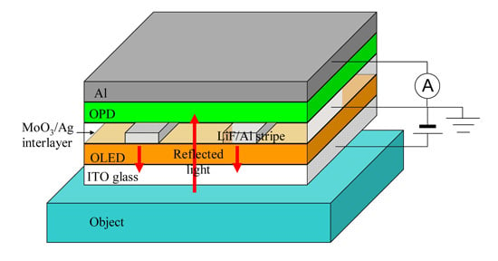
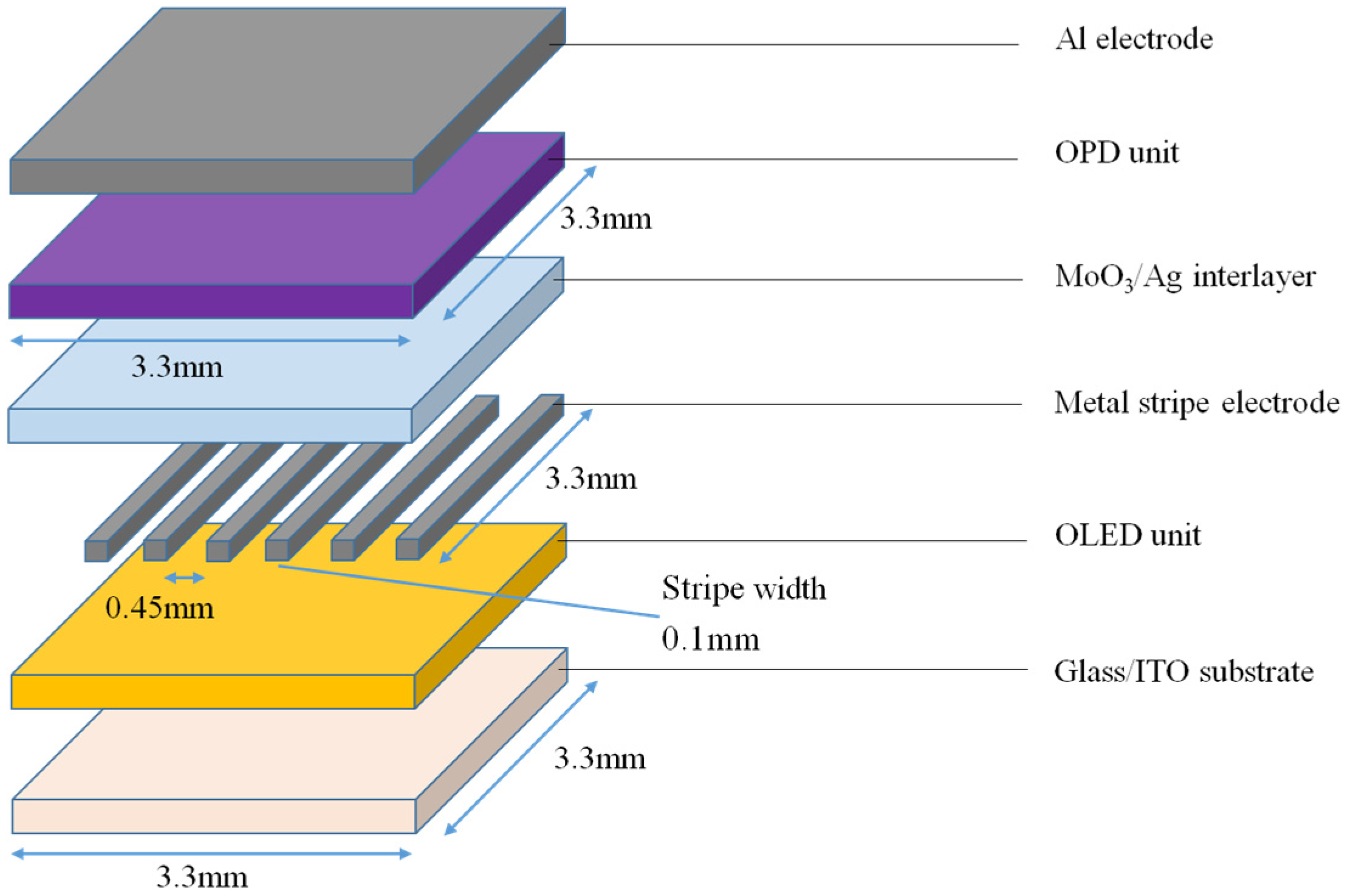
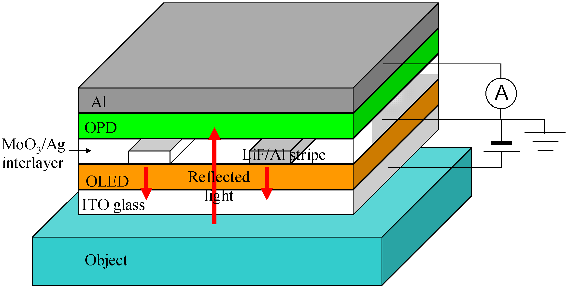
3.1. Operation Principle of the Organic Optical Sensor

The schematic diagram of the cross-sectional view of the integrated sensor is shown in Figure 1. Light emitted by the front OLED unit passes through the ITO/glass substrate and is reflected from the object underneath the glass substrate of the sensor. The reflected light is absorbed by the integrated OPD, with an active area between the stripe-shaped electrodes to generate the photocurrent signal. The change in photocurrent thus generated in the OPD is a function of the reflectivity of the object.
Figure 2 shows the top view of the electrode layout in the organic optical sensor. The width of the stripe-shaped cathode electrodes used for the OLED is 0.1 mm. The distance between the two adjacent stripe electrodes is 0.45 mm. A MoO3 (5 nm)/Ag (15 nm) bi-layer inter-electrode was overlaid on the stripe electrodes prior to the fabrication of the upper OPD. The region between the opaque area of the stripe electrodes defines the active area of the OPD, e.g., 2.7 mm × 4.15 mm in this case, with an aperture ratio of ~81%. The bi-layer inter-electrode serves a dual purpose to act as the cathode for the front OLED and an anode for the upper OPD. The emission comes from the stripe-shaped OLED; it prevents the OLED emission from going directly to the OPD, hence maintaining a high signal-to-noise ratio.
Figure 1. Schematic diagram of the organic optical sensor based on monolithic integration of OLED and OPD units, showing the operation principle of the sensor.
Electronics 04 00623 g001
Figure 2. Schematic layout of the stripe-shaped front OLED components and the upper OPDs covered in regions between the stripes in the organic optical sensor.
Electronics 04 00623 g002

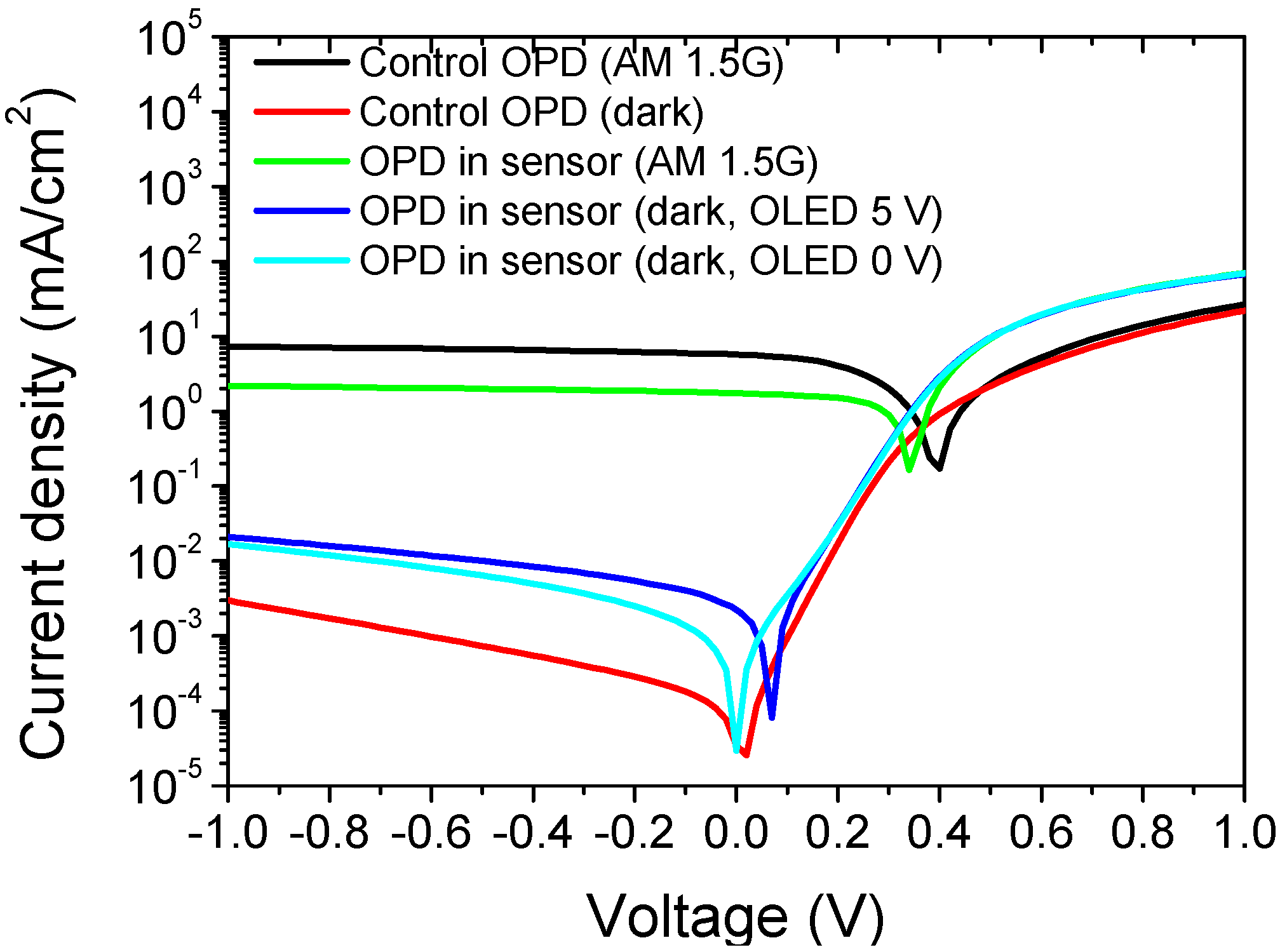
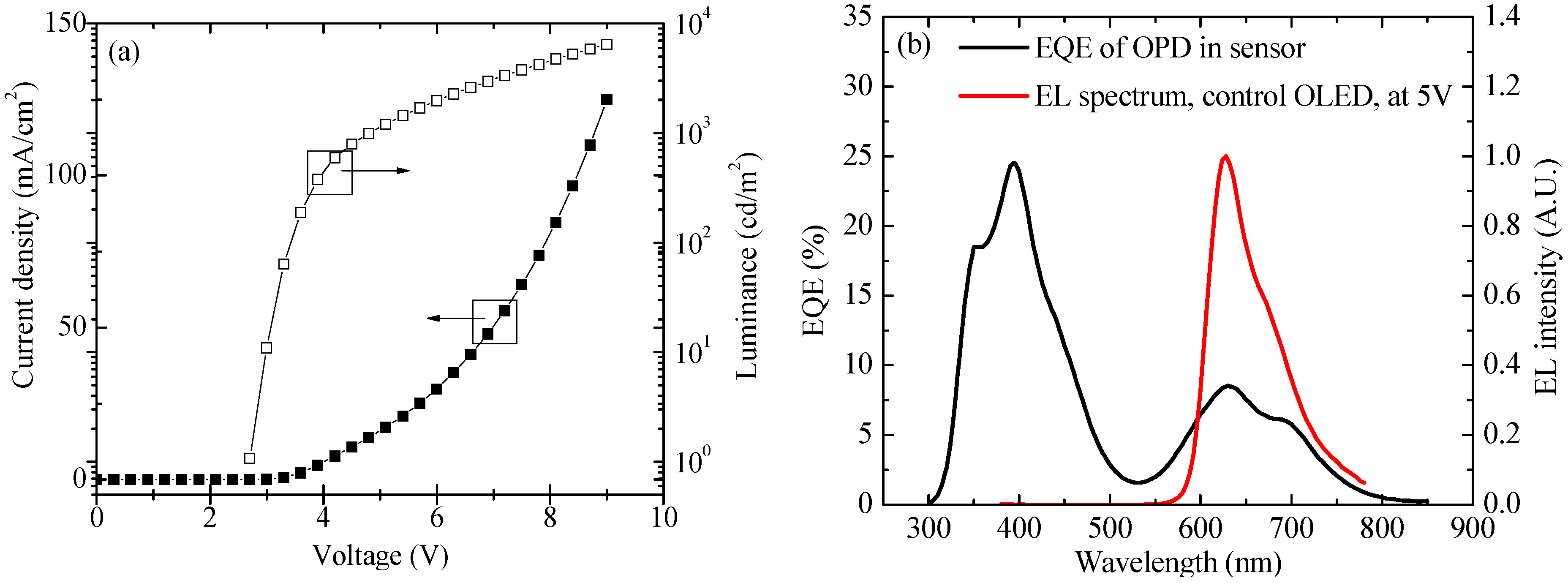
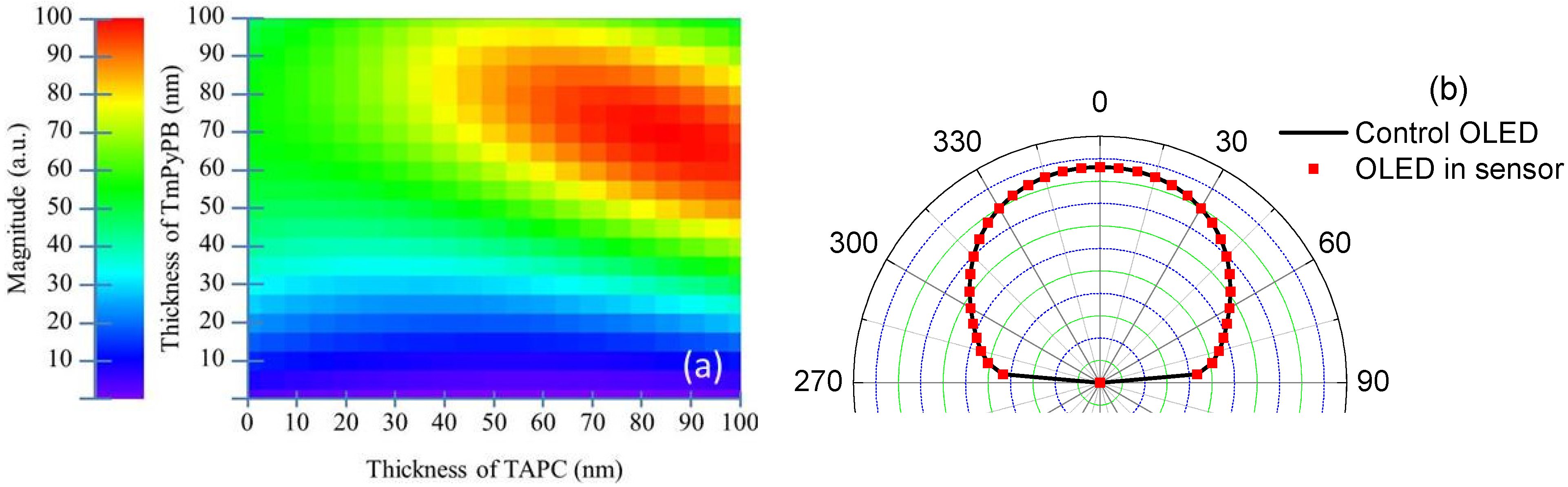
3.2. Characteristics of the OPD and OLED Units

The J-V characteristics measured for the OPD in the organic optical sensor and a control OPD, measured under AM1.5G irradiation of 100 mW/cm2, are shown in Figure 3. The control OPD had a short-circuit current density of 4.27 mA/cm2. The corresponding value for the OPD in the organic optical sensor was 1.6 mA/cm2. The dark photocurrent density of the OPD in the integrated sensor measured in the dark is considered as the noise or the reference. The photocurrent generated by the OPD when the OLED is emitting light and a light-reflecting object is placed in front of the sensor is then considered as the signal. The integrated organic optical sensor is designed to simultaneously achieve a high extraction of light emitted by the OLED unit and a high spectral responsivity of the OPD in the sensor, thereby increasing the signal-to-noise ratio. For comparison, the J-V characteristics of both the OPD in the organic optical sensor and the control OPD measured under AM1.5G and in the dark are also plotted in Figure 3 for comparison. The results show that OPD has a low noise or dark current density of <3.0 × 10⁻⁵ mA/cm2. It has a photocurrent density of ~2.0 × 10⁻³ mA/cm2, measured for the integrated OLED unit operated at 5.0 V, without an object present in the front of the organic optical sensor.
Figure 3. J-V characteristics measured for the control OPD and the OPD in the integrated organic optical sensor.
Electronics 04 00623 g003
As the width of the stripe-shaped OLED components in the organic optical sensor is only 100 μm, the performance of the OLED in the organic optical sensor was then evaluated using a control OLED with an active area of 3.3 mm × 3.3 mm. The J-V-L characteristics, luminous efficiency, and EL spectrum measured for the control OLED are given in Figure 4. The luminance and luminous efficiency of the control OLED operated at 5 V are 1200 cd/m2 and 7 cd/A, respectively. From Figure 4b it can be seen that the normalized EL spectrum for the control OLED has a peak wavelength at 628 nm with a full-width-half-maximum of 78 nm, which matches well with the spectral response of the ZnPc:C60-based OPD over the wavelength range from 520 nm to 750 nm. This ensures a good coupling between the EL emission of the OLED and the spectral response of the OPD in the organic optical sensor.
The thicknesses of the functional organic layers in the OPD and OLED were optimized to achieve the maximum photo response of the integrated organic sensor [21,22]. In the organic optical sensor, the reflected light enters into the OPD through the MoO3/Ag interlayer. The critical angle of the incident light at the MoO3/Ag interface is ~4 degrees due to a significant change in the refractive index between MoO3 (n = 1.86, at 625 nm) and Ag (n = 0.13, at 625 nm). Therefore, the reflected light with a small angle normal to the surface can be detected by the OPD unit in the integrated organic sensor. Enhancement in light out-coupling in the normal direction from the OLED, therefore, helps enhance the signal/noise ratio of the sensor. For the planar front OLED, most of the light is trapped inside the OLED due to the different waveguide losses in the substrate and organic layers and the surface plasmon polariton modes at the metal/organic interface. The enhancement in light out-coupling was realized by optimizing the thickness of the hole transporting and electron transporting layers in the integrated sensor.
Figure 4. (a) Current density-voltage and luminance-voltage characteristics of the control OLED; (b) EL spectrum of the control OLED and external quantum efficiency (EQE) of the integrated OPD.
Electronics 04 00623 g004
In this work, the optical admittance analysis was used for analyzing the emission behavior of the OLED in the organic sensor. In the optical simulation, it is assumed that the multi-layered OLED possesses a smooth interface between the adjacent layers. The point dipole emission characteristics were used in the simulation. The spatial dimension of the dipoles is considered rather small in comparison with the wavelength of the radiation as well as the space between the emitter and the individual interfaces in the OLED. As an approximation, the orientation of emitting molecules is isotropic with homogeneous emission in all directions in the OLED. In the organic optical sensor, the front OLED is optimized to achieve the maximum output luminance as illustrated in Figure 5a, thus producing an optimized signal/noise ratio of the sensor. In addition, the angular-dependent emissions of the control OLED (solid line) and OLED in the sensor (red square symbol) are also shown in Figure 5b. It is clear that the angular-dependent emissions of the control OLED and the OLED unit in the integrated sensor are very similar.
Figure 5. (a) The calculated normalized EL output of the control OLED and the OLED in the sensor, in the normal direction, as a function of the thickness of the TAPC hole transport layer and the TmPyPB electron transport layer. The color shown in the vertical bar in the plot indicates the magnitude of luminance (arb. unit); (b) The spatial emission profiles of the control OLED (solid line) and OLED unit (red square symbol) in the organic optical sensor.
Electronics 04 00623 g005

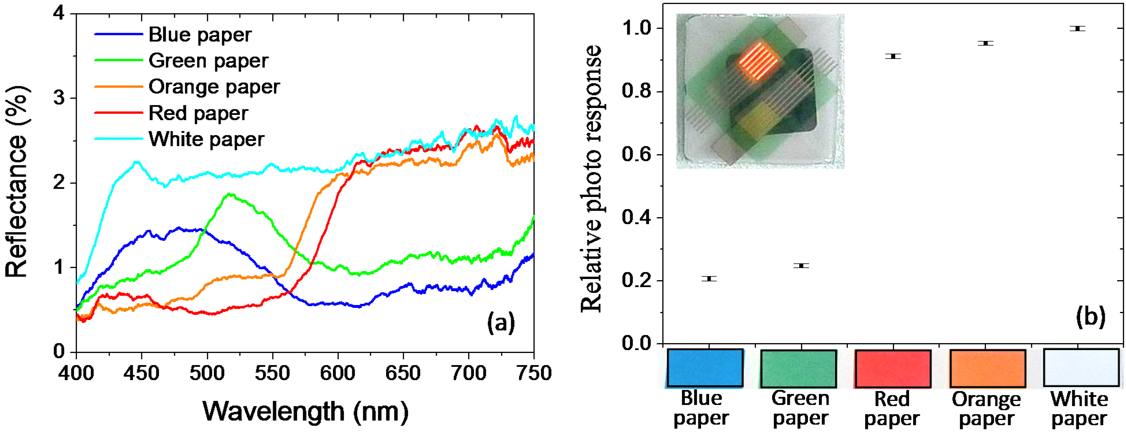
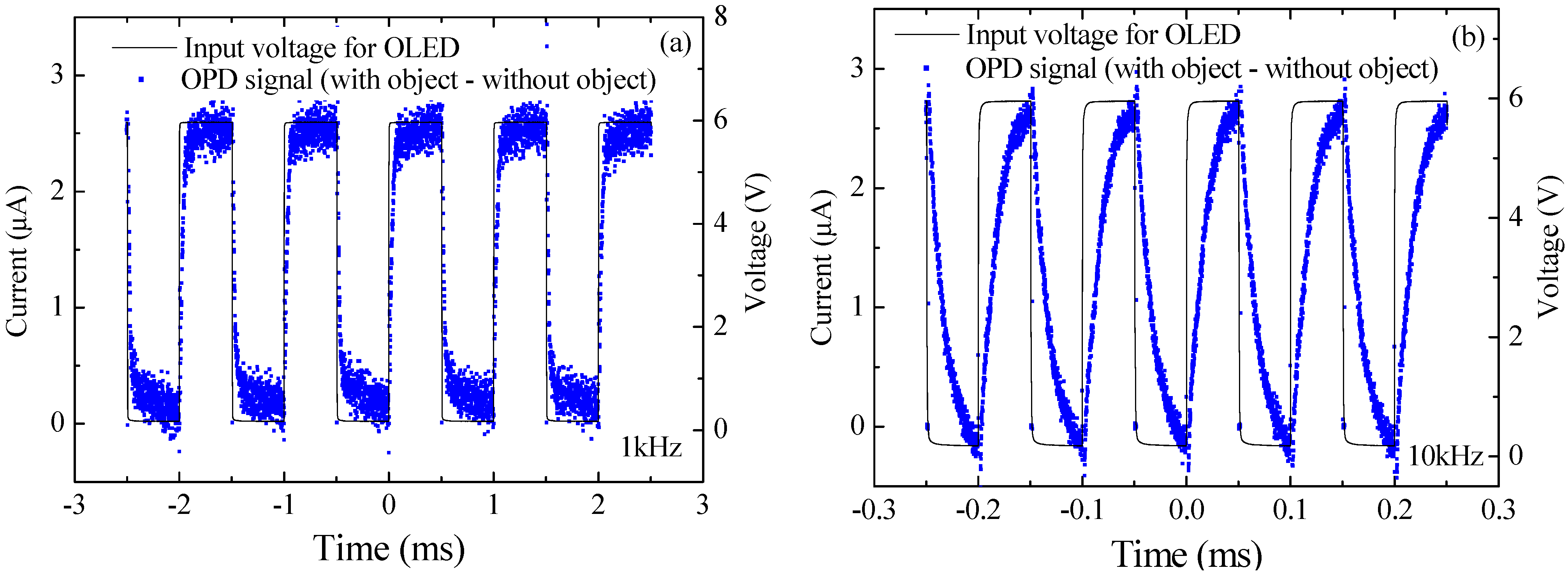
3.3. Photo Responses and Frequency Responses of the Organic Optical Sensor

To demonstrate the performance of the organic optical sensor, the photo responses of the sensor measured for objects with different reflections were recorded by measuring the photocurrent of the OPD with the OLED operated at 5 V. Figure 6 showed the normalized photo responses of the OPD in the organic optical sensor measured for objects with different reflection surfaces including white paper, orange paper, red paper, green paper, and blue paper. In this work, the EL emission of the OLED component in the sensor has a peak wavelength of 628 nm. White paper, orange paper, and red paper have relative higher reflection to the red illumination than that reflected from the green paper and blue paper, which is shown in Figure 6a. The measured photo responses of the organic optical sensor therefore follow the order of white paper, orange paper, red paper, green paper, and blue paper, as illustrated in Figure 6b.
Figure 6. (a) The reflection spectra measured for the different reflection surfaces of white paper, orange paper, red paper, green paper, and blue paper; (b) Normalized photo responses of the organic optical sensor measured for different colored paper placed underneath the sensor.
Electronics 04 00623 g006
The response time of the organic optical sensor was characterized by the frequency response of the OPD with the integrated OLED operated with a square wave pulse voltage, generated by a functional generator with an output modulated at 1 kHz or 10 kHz and amplitude of around 6 V. A sheet of white paper was placed in the front of the organic optical sensor to reflect the modulated OLED emission back to the OPD for frequency response measurements. The photocurrent generated in the OPD was estimated by measuring the voltage across a 1 kΩ resistor, connected in parallel with the OPD unit in the integrated sensor. Figure 7 shows the time response measurement results for the organic optical sensor. It is clear that the photo response of the OPD can be clearly identified for frequencies up to 10 kHz.
In the time response measurement, the OLED was operated with a square wave voltage, generated by a functional generator with an output modulated at different frequencies. The pulsed light from the OLED unit provides a binary output (with and without light) light source. In this way, light emitted from the OLED is modulated to a frequency designated by the functional generator. The photocurrent of the OPD, with the white paper placed in the front of the organic sensor, was measured using an oscilloscope to capture the photo response. By evaluating the current response of the OPD at different frequencies of the modulated OLED output, the speed of the signal response for the OPD can then be characterized. The decay and rise components in the time response profiles, shown in Figure 7, reflect the modulation speed of the OPD in the organic sensor, following an exponential characteristic, which is a function of the resistive-capacitive time constant of the measurement system. The results in Figure 7 demonstrate that the organic optical sensor, based on the monolithic integration of ZnPc:C60-based OPD and CBP:Ir(piq)2acac-based phosphorescent OLED, is capable of signal processing up to a 10 kHz regime.
Figure 7. Typical time response profile for the integrated ZnPc:C60-based OPD and CBP:Ir(piq)2acac-based phosphorescent OLED, operated by square wave pulse voltage (~6 V) with different frequencies of (a) 1 kHz and (b) 10 kHz.
Electronics 04 00623 g007
The organic optical sensor based on the integrated organic light transmissible devices, such as OPDs and OLEDs, provides the functional superiority for a broad range of applications. The integrated device uses OLED as light source for illumination of the coupled OPD to create an optical signal. Such an integrated organic sensor can be a building block for application in optical and waveguide sensors. The design and fabrication flexibility provided by the organic semiconductors and processes also have significant cost benefits, making it possible for new application in finger print identification, image sensors, and other organic photonic logical circuits and monitoring sensors.

4. Conclusions

The monolithic integration of organic components forming an OPD/OLED functional system for sensor application has been demonstrated. The performance of the functional organic sensors was analyzed, relating to the optimization of light coupling between the OLED and OPD components, as well as the examination of the optical and frequency responses. It reveals that the organic sensors are capable of signal processing in the 10 kHz regime. The design and fabrication flexibility provided by the material and process could readily construct multilayered organic sensor arrays for application in wearable units, disposable point of diagnosing, low cost bioassay devices, lab-on-chip, and vital sign monitoring and compact information systems.

Acknowledgments

This work was supported by Research Grants Council of the Hong Kong Special Administrative Region, China, Project No. T23-713/11, GRF12303114, the National Natural Science Foundation of China (Grant No. 61275037), HKBU MPCF project KTO-MPCF-07-2015/16, Hong Kong Baptist University Faculty Research Grant FRG2/14-15/081 and Strategic Development Fund SDF13-0531-A02.

Author Contributions

F.R.Z. directed the project. The experiments were carried by H.L.T. and W.H.C. The manuscript was written through contributions of all authors. All authors have given approval to the final version of the manuscript.

Conflicts of Interest

The authors declare no conflict of interest.

References

  1. Tang, C.W.; VanSlyke, S.A. Organic electroluminescent diodes. Appl. Phys. Lett. 1987, 51, 913–915. [Google Scholar] [CrossRef]
  2. Choi, W.H.; Tam, H.L.; Zhu, F.R.; Ma, D.G.; Sasabe, H.; Kido, J. High performance semitransparent phosphorescent white organic light emitting diodes with bi-directional and symmetrical illumination. Appl. Phys. Lett. 2013, 102, 153308. [Google Scholar] [CrossRef]
  3. Choi, W.H.; Tam, H.L.; Ma, D.G.; Zhu, F.R. Emission behavior of dual-side emissive transparent white organic light-emitting diodes. Opt. Express 2015, 23, A471–A479. [Google Scholar] [CrossRef] [PubMed]
  4. Tan, H.S.; Kulkarni, S.R.; Cahyadi, T.; Lee, P.S.; Mhaisalkar, S.G.; Kasim, J.; Shen, Z.X.; Zhu, F.R. Solution-processed trilayer inorganic dielectric for high performance flexible organic field effect transistors. Appl. Phys. Lett. 2008, 93, 183503. [Google Scholar] [CrossRef]
  5. Liu, H.X.; Wu, Z.H.; Hu, J.Q.; Song, Q.L.; Wu, B.; Tam, H.L.; Yang, Q.Y.; Choi, W.H.; Zhu, F.R. Efficient and ultraviolet durable inverted organic solar cells based on an aluminum-doped zinc oxide transparent cathode. Appl. Phys. Lett. 2013, 103, 043309. [Google Scholar] [CrossRef]
  6. Clark, J.; Lanzani, G. Organic photonics for communications. Nat. Photonics 2010, 4, 438–446. [Google Scholar] [CrossRef]
  7. Yao, Y.; Chen, H.Y.; Huang, H.; Yang, Y. Low voltage and fast speed all-polymeric optocouplers. Appl. Phys. Lett. 2007, 90, 053509. [Google Scholar] [CrossRef]
  8. Dong, G.; Zheng, H.; Jiang, C.; Duan, L.; Wang, L.; Qiu, Y. High-Performance Organic Optocouplers Based on a Photosensitive Interfacial C60/NPB Heterojunction. Adv. Mater. 2009, 21, 2501. [Google Scholar]
  9. Stathopoulos, N.A.; Palilis, L.C.; Vasilopoulou, M.; Botsialas, A.; Falaras, P.; Argitis, P. All-organic optocouplers based on polymer light-emitting diodes and photodetectors. Phys. Stat. Sol. 2008, 205, 2522–2525. [Google Scholar] [CrossRef]
  10. Hofmann, O.; Miller, P.; Sullivan, P.; Jones, T.S.; de Mello, J.C.; Bradley, D.D.C.; de Mello, A.J. Thin-film organic photodiodes as integrated detectors for microscale chemiluminescence assays. Sens. Actuators B 2005, 106, 878–884. [Google Scholar]
  11. Shinar, J.; Shinar, R. Organic light-emitting devices (OLEDs) and OLED-based chemical and biological sensors: An overview. J. Phys. D 2008, 41, 133001. [Google Scholar] [CrossRef]
  12. Choudhury, B.; Shinar, R.; Shinar, J. Glucose biosensors based on organic light-emitting devices structurally integrated with a luminescent sensing element. J. Appl. Phys. 2004, 96, 2949–2954. [Google Scholar] [CrossRef]
  13. Ratcliff, E.L.; Veneman, P.A.; Simmonds, A.; Zacher, B.; Huebner, D.; Saavedra, S.S.; Armstrong, N.R. A planar, chip-based, dual-beam refractometer using an integrated organic light-emitting diode (OLED) light source and organic photovoltaic (OPV) detectors. Anal. Chem. 2010, 82, 2734–2742. [Google Scholar] [CrossRef] [PubMed]
  14. Forrest, S.R. The path to ubiquitous and low-cost organic electronic appliances on plastic. Nature 2004, 428, 911–918. [Google Scholar] [CrossRef] [PubMed]
  15. Ramuz, M.; Bürgi, L.; Stanley, R.; Winnewisser, C. Coupling light from an organic light emitting diode (OLED) into a single-mode waveguide: Toward monolithically integrated optical sensors. J. Appl. Phys. 2009, 105, 084508. [Google Scholar] [CrossRef]
  16. Ali, F.; Periasamy, N.; Patankar, M.P.; Narasimhan, K.L. Integrated Organic Blue LED and Visible-Blind UV Photodetector. J. Phys. Chem. C 2011, 115, 2462–2469. [Google Scholar] [CrossRef]
  17. Lee, T.W.; Noh, T.Y.; Choi, B.K.; Kim, M.S.; Shin, D.W.; Kido, J. High-efficiency stacked white organic light-emitting diodes. Appl. Phys. Lett. 2008, 92, 043301. [Google Scholar] [CrossRef]
  18. Liao, L.S.; Klubek, K.P.; Tang, C.W. High-efficiency tandem organic light-emitting diodes. Appl. Phys. Lett. 2004, 84, 167. [Google Scholar] [CrossRef]
  19. Yakimov, A.; Forrest, S.R. High photovoltage multiple-heterojunction organic solar cells incorporating interfacial metallic nanoclusters. Appl. Phys. Lett. 2002, 80, 1667. [Google Scholar] [CrossRef]
  20. Peumans, P.; Forrest, S.R. Efficient, high-bandwidth organic multilayer photodetectors. Appl. Phys. Lett. 2000, 76, 3855. [Google Scholar] [CrossRef]
  21. Tam, H.L.; Wang, X.Z.; Zhu, F.R. Integration of transmissible organic electronic devices for sensor application. Proc. SPIE 2013, 8831, 883121. [Google Scholar]
  22. Wang, X.Z.; Tam, H.L.; Yong, K.S.; Chen, Z.K.; Zhu, F.R. High performance optoelectronic device based on semitransparent organic photovoltaic cell integrated with organic light-emitting diode. Org. Electron. 2011, 12, 1429–1433. [Google Scholar] [CrossRef]
  23. Matsushita, Y.; Shimada, H.; Miyashita, T.; Shibata, M.; Naka, S.; Okada, H.; Onnagawa, H. Organic bi-function matrix array. Jpn. J. Appl. Phys. 2005, 44, 2526–2829. [Google Scholar] [CrossRef]
  24. Xue, J.G.; Forrest, S.R. Organic optical bistable switch. Appl. Phys. Lett. 2003, 82, 136. [Google Scholar] [CrossRef]
  25. Ohmori, Y.; Kajii, H.; Kaneko, M.; Yoshino, K.; Ozaki, M.; Fujii, A.; Hikita, M.; Takenaka, H.; Taneda, T. Realization of polymeric optical integrated devices utilizing organic light-emitting diodes and photodetectors fabricated on a polymeric waveguide. IEEE J. Sel. Top. Quantum Electron. 2004, 10, 70–78. [Google Scholar] [CrossRef]
  26. Low, B.L.; Zhu, F.R.; Zhang, K.R.; Chua, S.J. An in situ sheet resistance study of oxidative-treated indium tin oxide substrates for organic light emitting display applications. Thin Solid Films. 2002, 417, 116. [Google Scholar] [CrossRef]

