1. Introduction
Organic molecular solids, such as organic semiconductors, have been studied intensively due to their considerable scientific and industrial uses. The pristine electronic properties of such material ensures good insulation because of the closed-shell structure of organic molecules, but they can also become electric conducting materials when a charge accumulation layer is formed by the application of an electric field on the surface. The π-electrons, whose interaction is described by weak van-der-Waals interaction, are responsible for the charge transport, in sharp contrast to those in inorganic semiconductors with a well-defined covalent network for charges to transfer. Hence, organic semiconductors have often seemed to provide poor electric conductivity and it appears that the hopping transport mechanism is realized on the basis of localized electronic states. Nevertheless, it has been revealed that some of the organic semiconductor systems show moderate carrier mobility above 1 cm
2/Vs [
1,
2,
3,
4] and the charge transport mechanism is dominated by a band transport system described by spatially-distributed Bloch waves similar to ordinary metals, but on the verge of self-localization because of the strong molecular fluctuation [
5]. From a microscopic viewpoint, the peculiar shape of molecular orbitals in such compounds causes condensation in the corresponding crystal structure at ambient pressure as a result of naïve balance between mutually attracting London force and Coulomb repulsive force. Therefore, considerable impact is expected with the application of external pressure, not only by reducing molecular distance but also by deforming the crystal structure due to freedom of onsite molecular orientation. This is essentially different from inorganic semiconductors composed of atoms which appear as a spherical mass point. Therefore the application of external pressure is expected to induce a striking change in not only simple reduction of intermolecular molecule distance, but also the deformation of the crystal structure due to the freedom of onsite molecular orientation, and the unanticipated pressure response of electronic properties unlike a simple linear increase in charge transfer rate. Looking at the current progress the electronic industry is making in organic semiconductors, this kind of work becomes necessary for the development of flexible and soft-printed organic devices which is subjected to a bending force behaving like pressure.
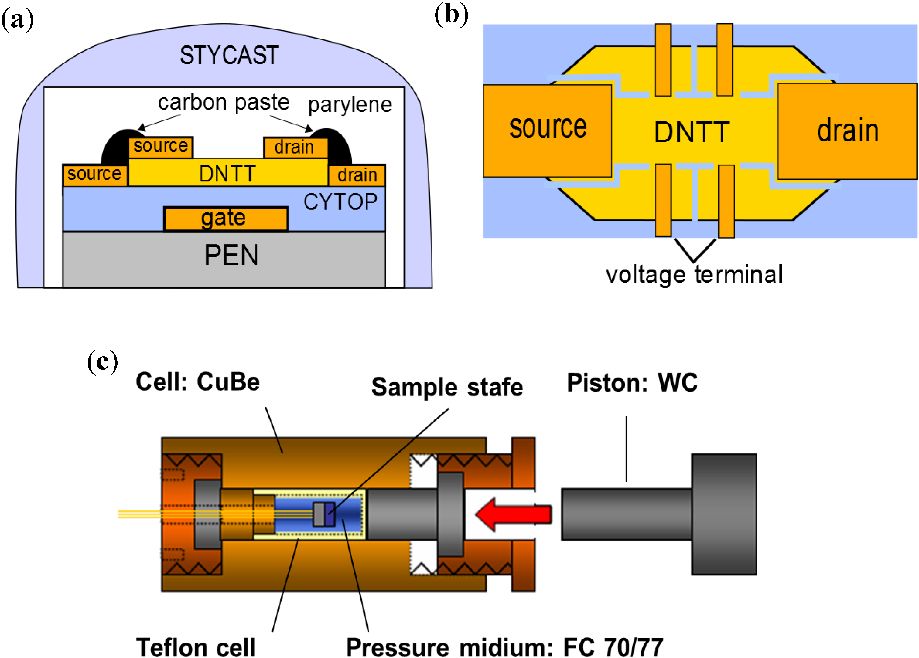
In this paper we introduce a method of measuring the effect of hydrostatic pressure on charge carrier conductivity in organic semiconductor crystals, introducing the charge with the application of an electric field on the semiconductor surfaces. In addition to the measurement of common transfer characteristics of drain current as a function of gate voltage shown in former pioneering studies [
6,
7], we performed four-terminal conductivity measurements to exclude extrinsic influences of metal-to-semiconductor contact resistance [
8]. In previous studies, carrier mobility
μ of hydrocarbons, such as rubrene, pentacene, were shown to exhibit a positive pressure response against external pressure
p, and their pressure coefficient, d
μ/d
p, is extremely larger than used in inorganic semiconductors. Here we focused on the pressure effect of one of heteroacene-based compounds, dinaphtho[2,3-
b:2',3'-
f]thieno[3,2-
b]thiophene (DNTT). It was found that DNTT shows far larger d
μ/d
p values whose sign can even be negative. The result cannot be explained by the simple model: increase in charge transfer rate with decreasing molecular distance. We note that the pressure effect of molecular solids can be explained by taking into account displacement, rotation and other degrees of freedom originating from molecular shapes. From an x-ray diffraction experiment, we constructed a plausible model of the pressure-induced structural deformation. In combination with the measurement of anisotropic charge transfer and structural studies, a route to study the so-called “structure-property relations” is provided [
9].
3. Results and Discussion
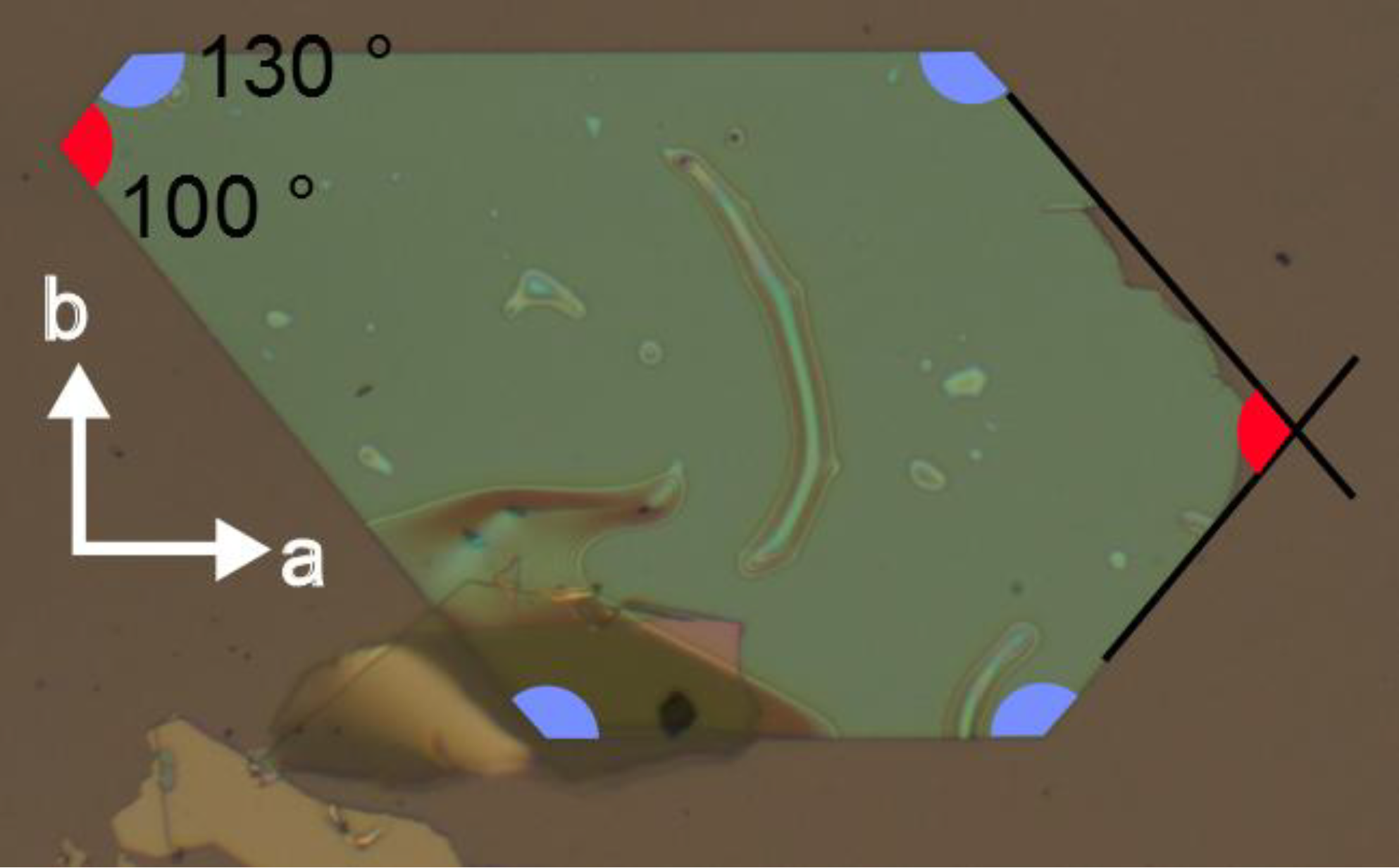
The unit cell of DNTT is monoclinic, meaning that there are four lattice parameters, lattice constants along
a,
b, and
c axes and an angle
β, defined as crossing angle of
a and
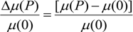
c axes. The XRD patterns as a function of 2
θ at each pressure point are shown in
Figure 3. No disappearance and emergence of peaks in pressurizing process is observed, indicating that there is no structural phase transition up to 2 GPa. Every peak shifts toward larger angle, indicating the overall shrinkage of unit cell. We choose four distinctive peaks assigned to (100), (003), (020) and (111) so that the four lattice parameters can be identified. Note that the result is consistent with the positions of all over visible peaks.
Figure 3.
XRD patterns for pressurized powder DNTT. Red, blue, green and dark arrows indicate (100), (003), (020) and (11-1) reflection peaks, respectively [
9].
Figure 3.
XRD patterns for pressurized powder DNTT. Red, blue, green and dark arrows indicate (100), (003), (020) and (11-1) reflection peaks, respectively [
9].
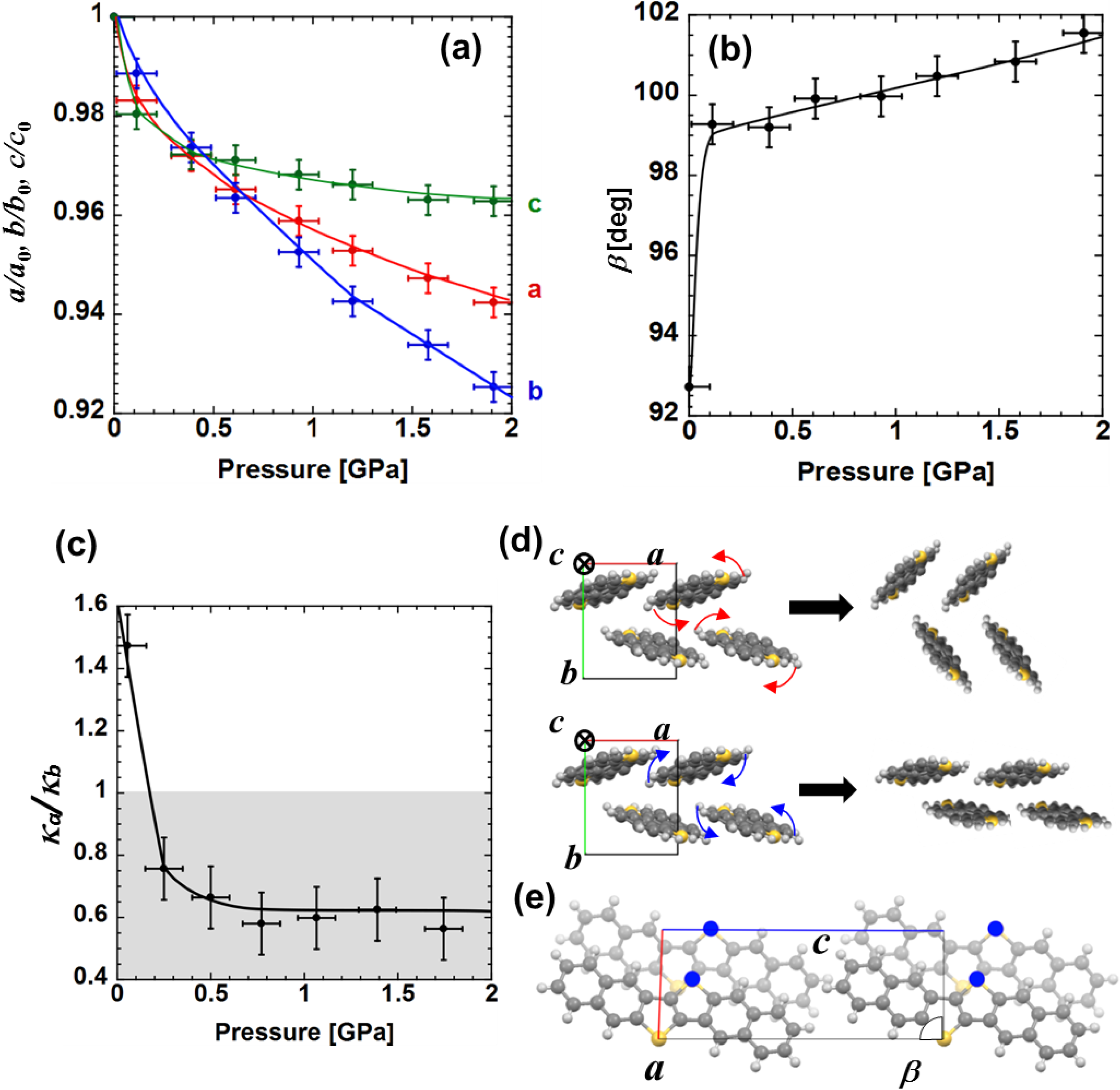
Figure 4a,b indicate the variations of these parameters as a function of pressure. It was found that the lattice parameters
a,
c and
β shows rapid variation at the lower pressure range (approximately less than 0.2 GPa) and then moves to more moderate pressure dependency at higher pressure range, in contrast to the variation of
b showing an almost constant rate. For further discussion consider the molecular rearrangement in the process of pressurization.
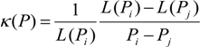
Figure 4c shows the ratio of compressibility in
a (κ
a) and
b (κ
b) directions. Here the compressibility is defined as the differential coefficient estimated from two adjacent measurement points,
where
Pi and
Pj are two adjacent pressure points (
Pi >
Pj).
L(
Pi) and
L(
Pj) are the lattice constants evaluated at each pressurized condition and
P is the average value between
Pi and
Pj, defined as (
Pi +
Pj)/2 for the sake of convenience since lattice constants plotted in present paper are discrete value; therefore
x-values of data points in
Figure 4a,c are deviated.
Figure 4.
Pressure dependence of (
a) lattice constants for three crystallographic directions and (
b)
β, defined as the intersection angle between
a and
c axes; (
c) Compressibility ratio between
a and
b axes as a function of applied pressure; (
d) Schematic diagram of suggested molecular rearrangement in
ab plane. The two pictures depict the molecular rearrangements in case of shrinkage along the
a and
b directions, respectively. Red and blue arrows indicate the rotation direction; (
e) Crystal structure in
ac plane. Dark and light molecular images and arrows indicate molecules located on the front and reverse side and corresponding displacement direction in pressurization process, respectively [
9].
Let us focus on the discussion of the pressure effect below approximately 0.2 GPa. Within this pressure range
κa/
κb is larger than 1, suggesting that the deformation of unit cell in
ab plane is dominated by the shrinkage along
a-axis. In this case molecules are supposed to be rearranged with concomitant rotation indicated by the curved red arrows in
Figure 4d. For a higher pressure range, the unit cell starts to shrink along
b-axis since
κa/
κb < 1, in which the molecules are supposed to start onsite rotation along the opposite direction to that in the lower pressure range (curved blue arrows in
Figure 4d). Note that the relationship between the dominant shrinkage direction of unit cell and the corresponding molecular rearrangement mentioned above is consistent with structural change experimentally observed in the oligoacene system, such as anthracene, pentacene and tetracene under high pressure [
12,
13].
It is noted that similar pressure dependences are shown among
a,
c and
β: drastic change in lower pressure region and the following slow change in higher pressure region (
Figure 4d). To approach this experimental result let us take into account the molecular rearrangement in
ac plane which is characterized by these three lattice parameters. As an external mechanical force is added intermolecular interaction is enhanced due to the access of nearest-neighbor molecules. The π-electrons tend to be localized on electro-negative sulfur atoms as compared to carbon and hydrogen sites [
14], in addition to the effect of spatially large occupation of the 3
pz orbitals on sulfur atoms. Therefore it is expected that intermolecular interaction of nearest-neighbor DNTT molecules are highly dominated by effects between sulfur atoms of different molecules. As the interaction between nearest-neighbor sulfur atoms marked by blue circles in
Figure 4e becomes large with increasing pressure, the adjacent molecules tend to displace along
c-axis to reduce the energy loss of Coulomb repulsion. Because sulfur-to-sulfur interaction is pronounced along
a-axis, both
c and
β parameters exhibit drastic change under relatively low pressure in the region of
κa/
κb > 1 where shrinkage of
a is dominant, while the values are less sensitive to pressure when shrinkage onn the
b-axis is dominant at higher pressure. The greater sulfur-to-sulfur interaction along the
a-axis than the
b-axis is also consistent with higher carrier mobility on the
a-axis compared to that along the
b-axis. Note that the change in
β up to 10° at around 2 GPa contrasts that observed in sulfur-free oligoacenes in which only a few degrees of deviation up to 10 GPa is observed for angles, so called
α,
β and
γ [
12,
13].
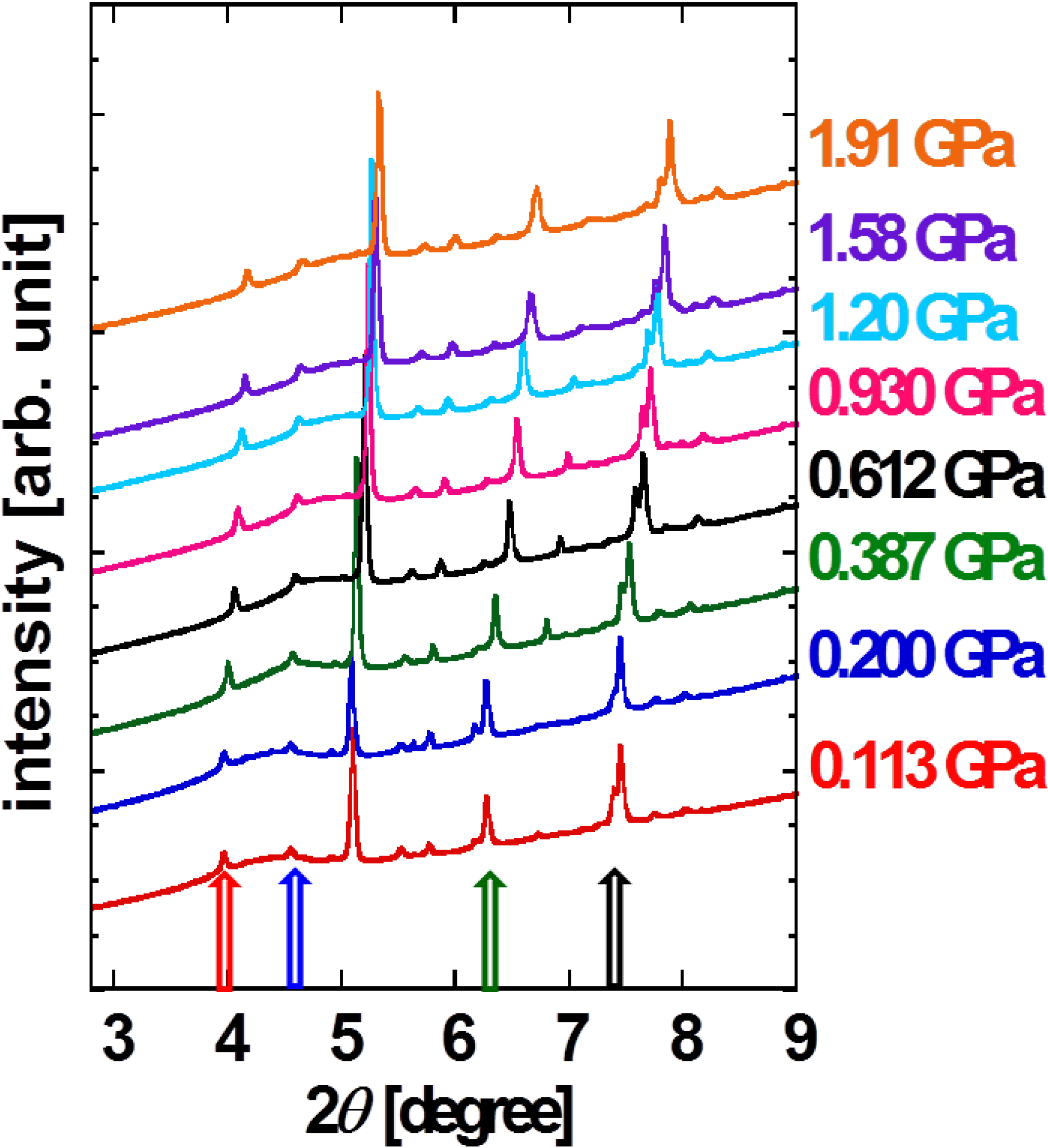
Pressure effects of carrier mobility in DNTT-FETs are measured along two distinctive crystallographic directions,
a- and
b-axes. Transport and output characters and carrier conductivity as a function of gate voltage are indicated in
Figure 5 for each axis. For quantitative discussion of pressure effects on carrier transport properties of DNTT-FETs, let us introduce the increasing rate defined as
where
μ(
P) and
μ(0) are four-terminal mobility at a certain pressure
P and that in the ambient condition. Note that estimated carrier mobility along each axis in ambient conditions is 2.1 cm
2/Vs for
a-axis and 1.3 cm
2/Vs for
b-axis respectively. This anisotropic value is in agreement with a previous report [
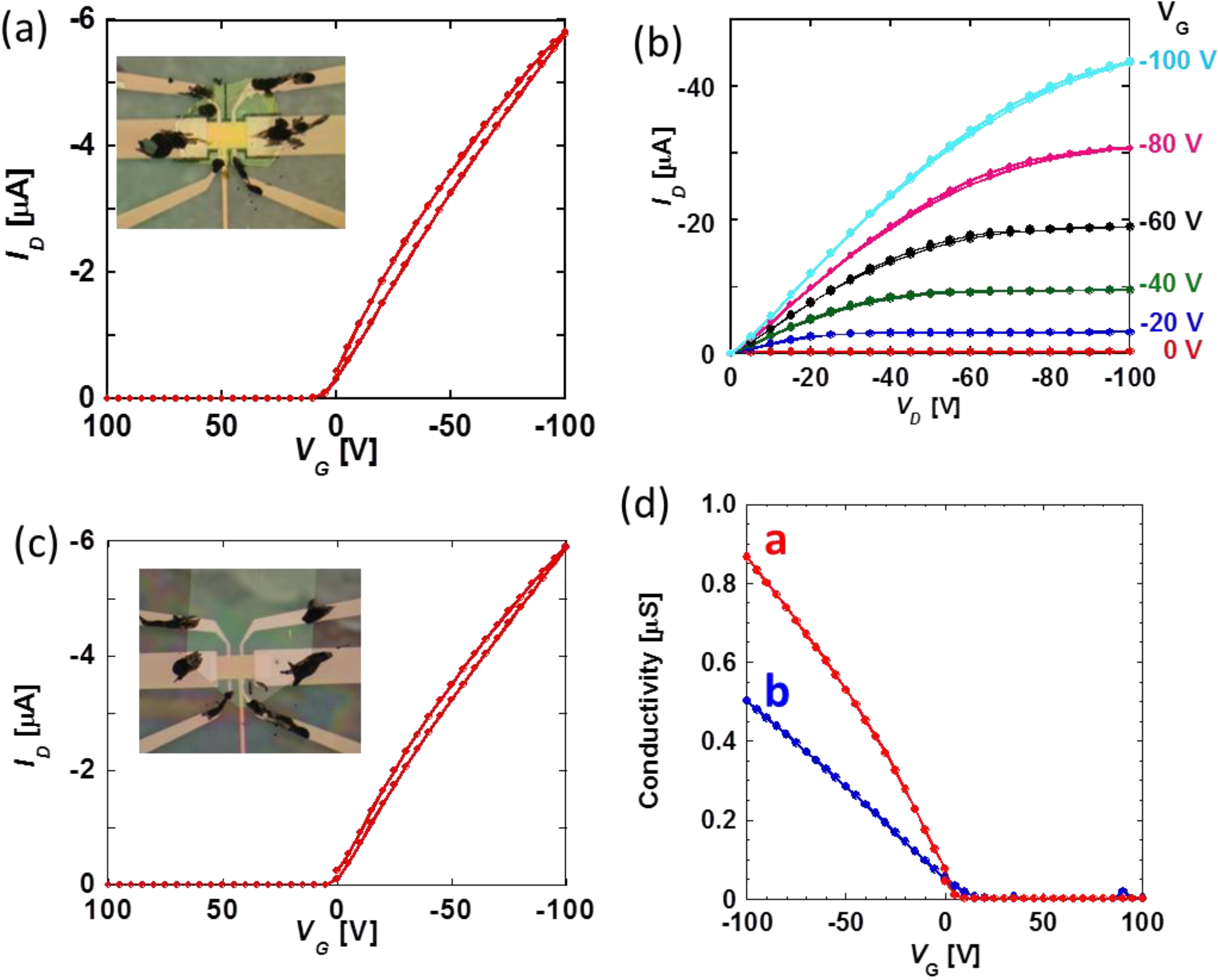
15]. The pressure dependence of carrier mobility is shown in
Figure 6 at the drain bias voltage
VD of −10 V. In the present study, the reproducibility of carrier mobility against compression and decompression is confirmed. Simultaneous plots of pressure-dependent carrier mobility of rubrene [
8] and pentacene [
16] devices reveal that carrier transport of DNTT is much more sensitive to pressurization and, furthermore, shows the nonmonotonous pressure response characterized by the appearance of peak and valley at 0.15 GPa on the
a-axis and
b-axis devices, respectively. Note that this is a quite different feature in contrast to two other hydrocarbon FETs with simple linear responses.
Figure 5.
(
a) Transport and (
b) output properties of DNTT-FET for
a-axis conducting direction; (
c) transport properties of DNTT-FET for
b-axis conducting direction. Photographs for each devices are inserted in (
a) and (
c); (
d) four-terminal conductivity in
a and
b-axes at ambient condition. The estimated carrier mobility is 2.1 cm
2 V
−1 s
−1 for
a-axis and 1.3 cm
2 V
−1 s
−1 for
b-axis at VG = −100 V, respectively [
9].
Figure 6.
Pressure effect on DNTT-FET for
a and
b-axes [
9]. Those for pentacene [
16] and rubrene [
8] devices are also plotted for comparison. Open and closed circles indicate the data obtained in compression and decompression processes.
Figure 6.
Pressure effect on DNTT-FET for
a and
b-axes [
9]. Those for pentacene [
16] and rubrene [
8] devices are also plotted for comparison. Open and closed circles indicate the data obtained in compression and decompression processes.
To assist in understanding this phenomenon, it is good to associate this problem with the structural variation by external pressure as shown in
Figure 4. The appearance of a peak in Δ
μ(
P)/
μ(
P) can be taken that the sign of the derivative d
μ/d
P for each axis is converted at 0.15 GPa, which coincides with the crossover point of
κa/
κb = 1, representing a simultaneous change in the anisotropic deformation of unit cell at the same pressure. Therefore the anomalous pressure response of carrier mobility on DNTT-FET seems to be connected with the change in molecular arrangement mentioned above. When
p < 0.15 GPa, our results suggest that the molecules are likely to rearrange so that face-to-face π–π stacking is enhanced along the
a-axis, which leads to the increase in carrier mobility on the
a-axis and decrease on the
b-axis. In contrast, when
p > 0.15 GPa, the structural change has the opposite effect, so that carrier mobility decreases on the
a-axis and increases on the
b-axis, respectively. Therefore the peak structure results from crossover between the two distinct molecular rotations associated with pressurization. At a higher pressure than 0.30 GPa, a slight increase in carrier mobility on the
a-axis can be seen due to the predominance of the normal pressure effect from the increase in density of molecular packing. Note that the contribution of molecular rearrangement is suppressed in the profile of Δ
μ(
P)/
μ(
P) in this pressure region. We have demonstrated the relationship of carrier transport properties and the structure of DNTT-FETs via their pressure response. However, for further elucidation of structure-property relations of pressure-sensitive organic semiconductors, crystal structure analysis under high pressure should be completed so that we complement the detailed information about the molecular rearrangement. The magnitude of pressure coefficient is up to 3.8 GPa
−1 along the
a-axis and is extremely large below 0.15 GPa as compared to those of rubrene (0.2 GPa
−1) and pentacene (0.4 GPa
−1), which is already one order larger than typical values for inorganic materials [
17]. In conjunction with the significant contribution of the sulfur-to-sulfur interaction which causes peculiar displacement in the
ac plane, the presence of sulfur atoms in DNTT is responsible for the anomalous pressure dependence in carrier mobility, indicating the significant contribution of 3
pz orbital on sulfur to the charge transport in the semiconductors and to the device performance. It is highly expected that the more efficient charge transfer on the
a-axis is realized in DNTT FETs by pressurization, due to the enhancement of orbital overlap, and especially the presence of more spatially-spread 3
pz orbital on sulfur atoms than those for carbon and hydrogen, the main components of rubrene and pentacene.
