1. Introduction
Many techniques that use an active auxiliary circuit to help the main switch of a single-switch pulse-width modulated (PWM) converter turn on with zero-voltage switching (ZVS) have been proposed [
1,
2,
3,
4,
5,
6,
7,
8,
9,
10,
11,
12,
13,
14,
15,
16,
17,
18,
19,
20,
21,
22,
23,
24,
25,
26,
27]. These techniques reduce switching losses in the main power switch, reduce reverse-recovery losses in the main power diode, and reduce EMI in the converter. The auxiliary circuit is typically placed parallel to the main switch (
Figure 1), and is activated just before the main converter switch is to be turned on.
The circuit gradually diverts current away from the main power diode to eliminate diode reverse recovery current after it is activated. It then discharges the capacitance across the main switch so that the switch can be turned on with ZVS. Finally, the circuit is deactivated from the main power circuit shortly after the main switch is turned on, so that the converter operates as a conventional PWM converter for the remainder of the switching cycle. The auxiliary circuit components have lower ratings than those in the main power circuit, as the circuit is active for only a small portion of the switching cycle. This allows a device that can turn on with fewer switching losses than the main switch to be used as the auxiliary switch.
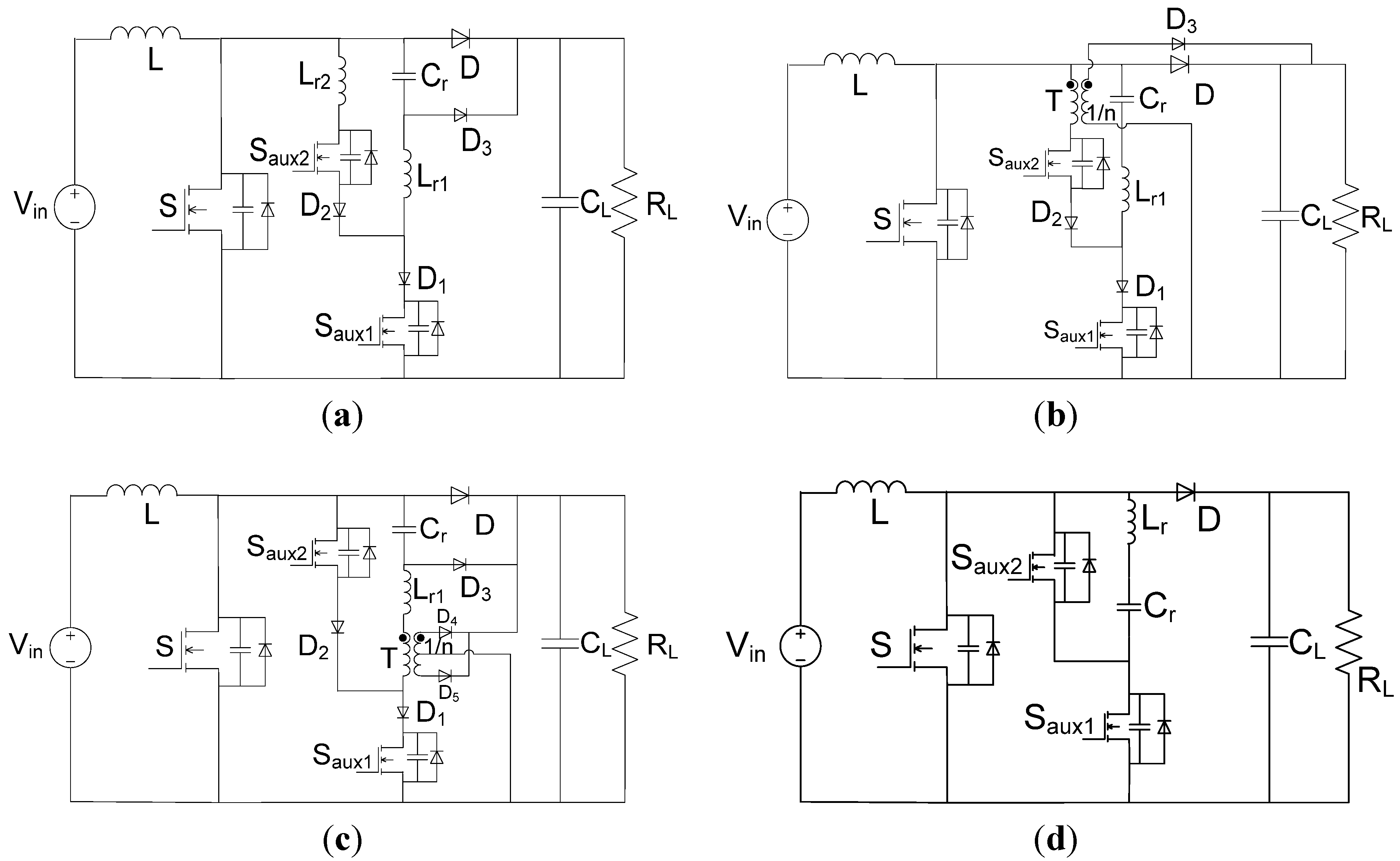
Figure 1.
Zero-voltage switching (ZVS)-pulse-width modulated (PWM) boost converters with auxiliary circuits. (
a) Non-resonant auxiliary circuit [
1]; (
b) Resonant auxiliary circuit [
11]; (
c) Dual auxiliary circuit [
16].
Figure 1.
Zero-voltage switching (ZVS)-pulse-width modulated (PWM) boost converters with auxiliary circuits. (
a) Non-resonant auxiliary circuit [
1]; (
b) Resonant auxiliary circuit [
11]; (
c) Dual auxiliary circuit [
16].
Previously proposed ZVS-PWM converters, however, have at least one of the following drawbacks:
The auxiliary switch is turned off while it is conducting current, which generates switching losses and EMI that offset the benefits of the auxiliary circuit [
1,
5,
7,
10,
13,
14,
22,
23].
The auxiliary circuit causes the main switch or boost diode to operate with higher peak current stress and more circulating current, which increases conduction losses and results in the need for a higher current-rated device for the main switch [
2,
3,
6,
8,
11,
12,
15,
21,
22,
23].
The auxiliary circuit components have high peak voltage stresses (at least twice the output voltage) and/or current stresses [
2,
3,
6,
8,
12].
Energy from the output, which contributes to circulating current and losses, must be placed into the auxiliary circuit to trigger a resonant process [
16,
17].
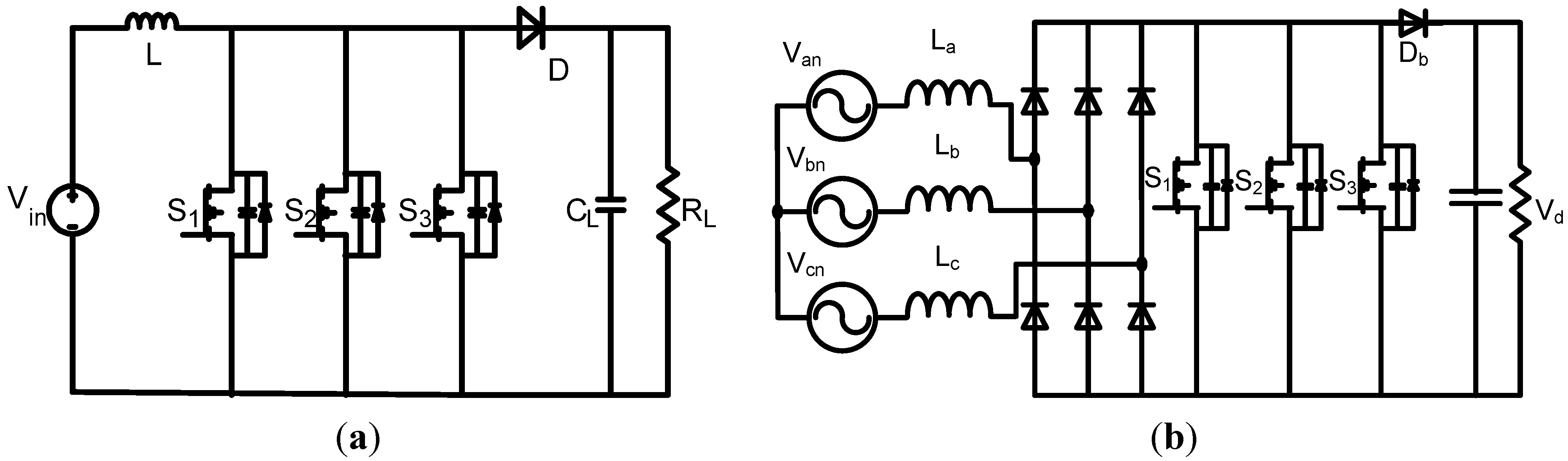
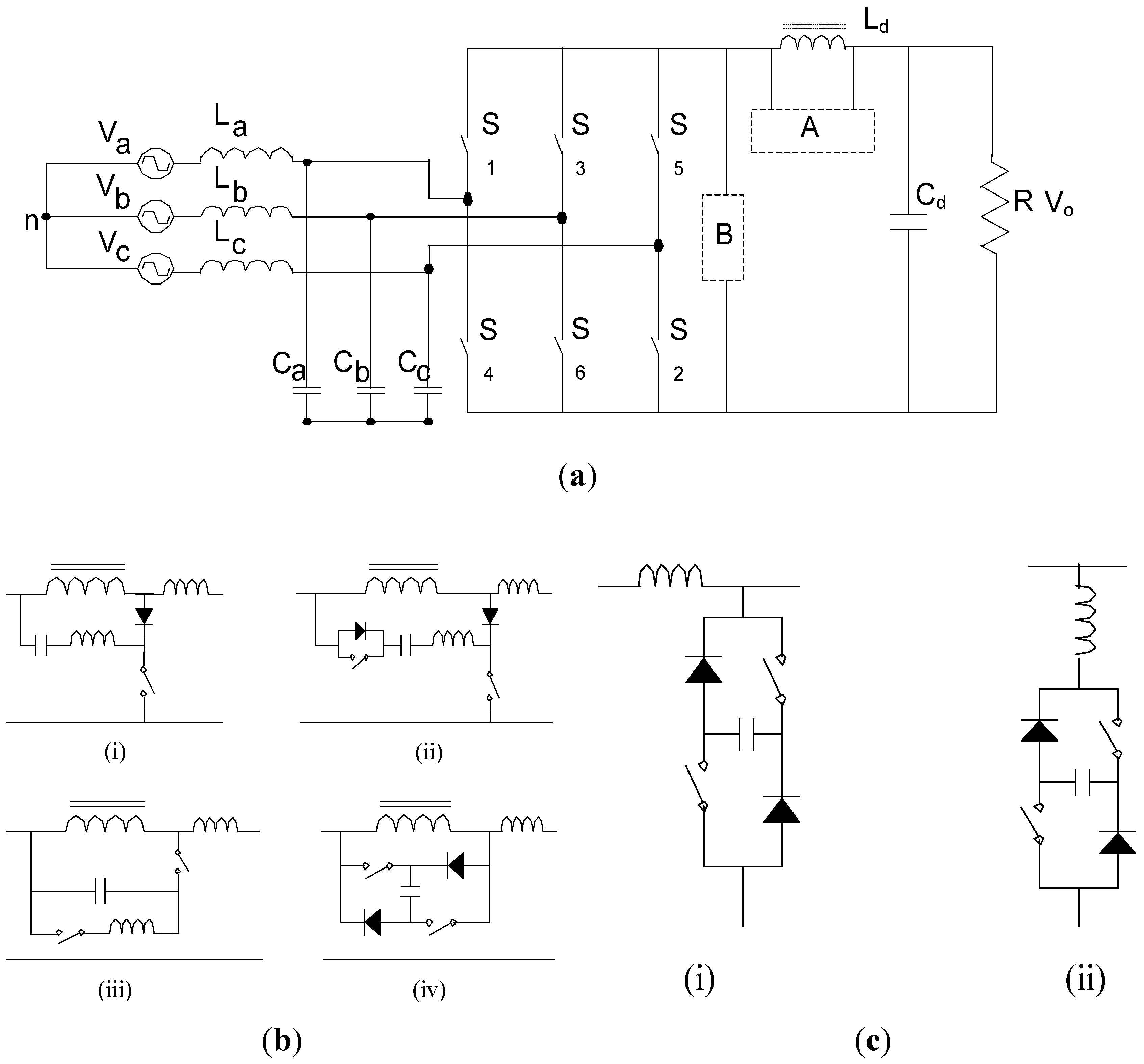
It is standard practice in industry to implement a PWM converter with several MOSFETs in parallel to reduce the on-state resistance of the main power switch and thus its conduction losses. Examples of such an implementation are shown in
Figure 2a,b for a DC-DC PWM boost converter and a three-phase AC-DC converter respectively. Although using a single IGBT as the boost switch may be cheaper, IGBTs cannot operate with switching frequencies as high as those that MOSFETs can so that the size of the magnetic and filtering components (and thus the converter size) cannot be made as small. Small converter size is necessary for industrial applications such as telecom power converters that are part of power systems that are placed in cabinets where space is a major issue. An auxiliary circuit can be used to reduce switching losses in a paralleled MOSFET converter that operates with higher power and current, but the above-mentioned drawbacks become worse than what they are for lower power converters.
Figure 2.
Converters with paralleled MOSFETs. (a) DC-DC boost converter; (b) Three-phase boost rectifier.
Figure 2.
Converters with paralleled MOSFETs. (a) DC-DC boost converter; (b) Three-phase boost rectifier.
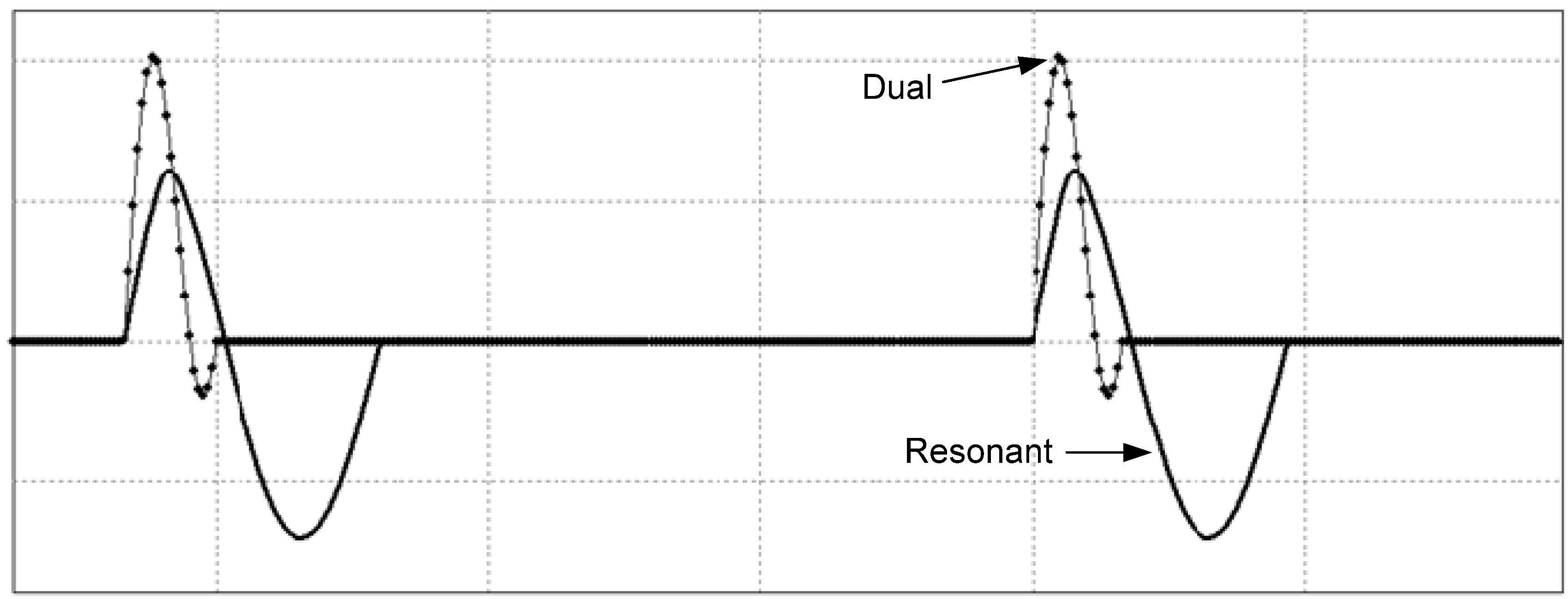
For example, the turn-off losses of the auxiliary switch in a converter with a non-resonant auxiliary circuit (
i.e.,
Figure 1a) are considerable. If resonant (
Figure 1b and dual
Figure 1c) approaches are used to ensure the soft turn-off of the auxiliary switch, then other problems arise, as can be seen from the auxiliary inductor waveforms shown in
Figure 3. The negative part of the waveform for the
Figure 1b circulates in the main switches and increases their peak stresses and conduction losses. The current waveform for the
Figure 1c converter (
ILr1) has an extremely high peak, at least double the input current, which makes it difficult to find an appropriate device for the auxiliary switch to carry this current.
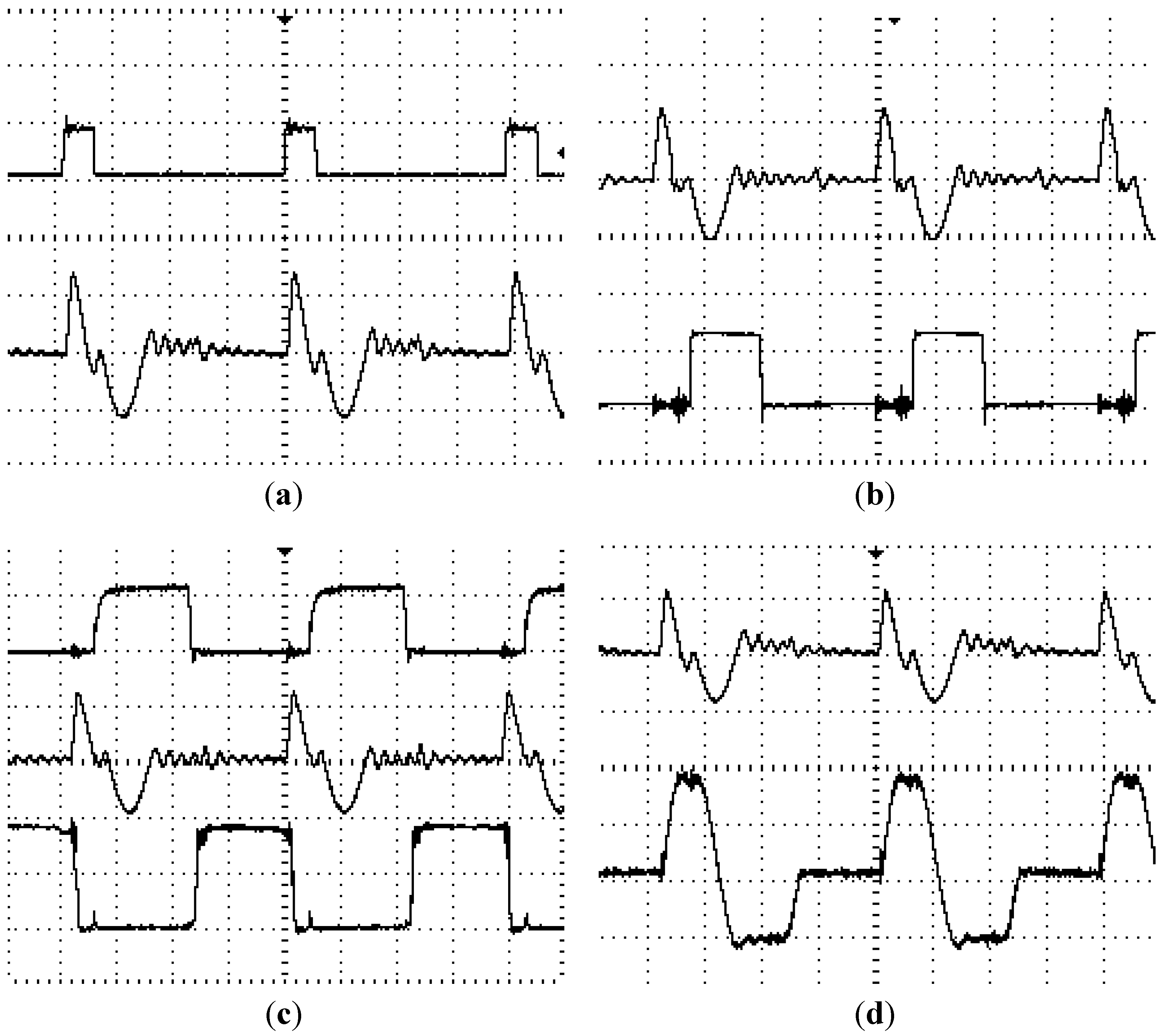
Figure 3.
Typical auxiliary inductor current waveforms for ZVS-PWM boost converters operating with input voltage Vin = 100 V, output voltage Vo = 400 V, output power Po = 2 kW, and switching frequency fsw = 100 kHz. Scale: I = 20A/div., Time: t = 5 μs/div.
Figure 3.
Typical auxiliary inductor current waveforms for ZVS-PWM boost converters operating with input voltage Vin = 100 V, output voltage Vo = 400 V, output power Po = 2 kW, and switching frequency fsw = 100 kHz. Scale: I = 20A/div., Time: t = 5 μs/div.
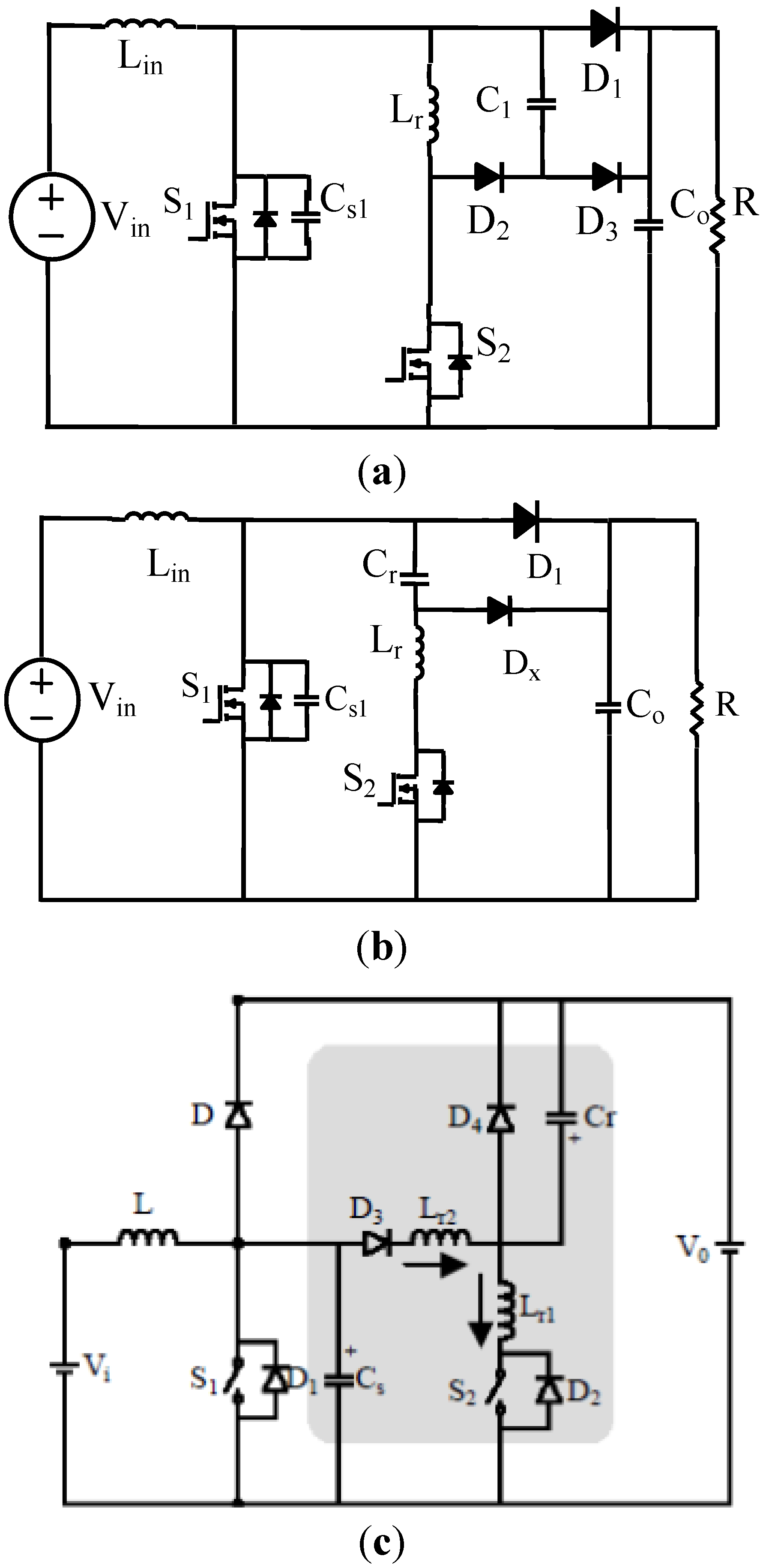
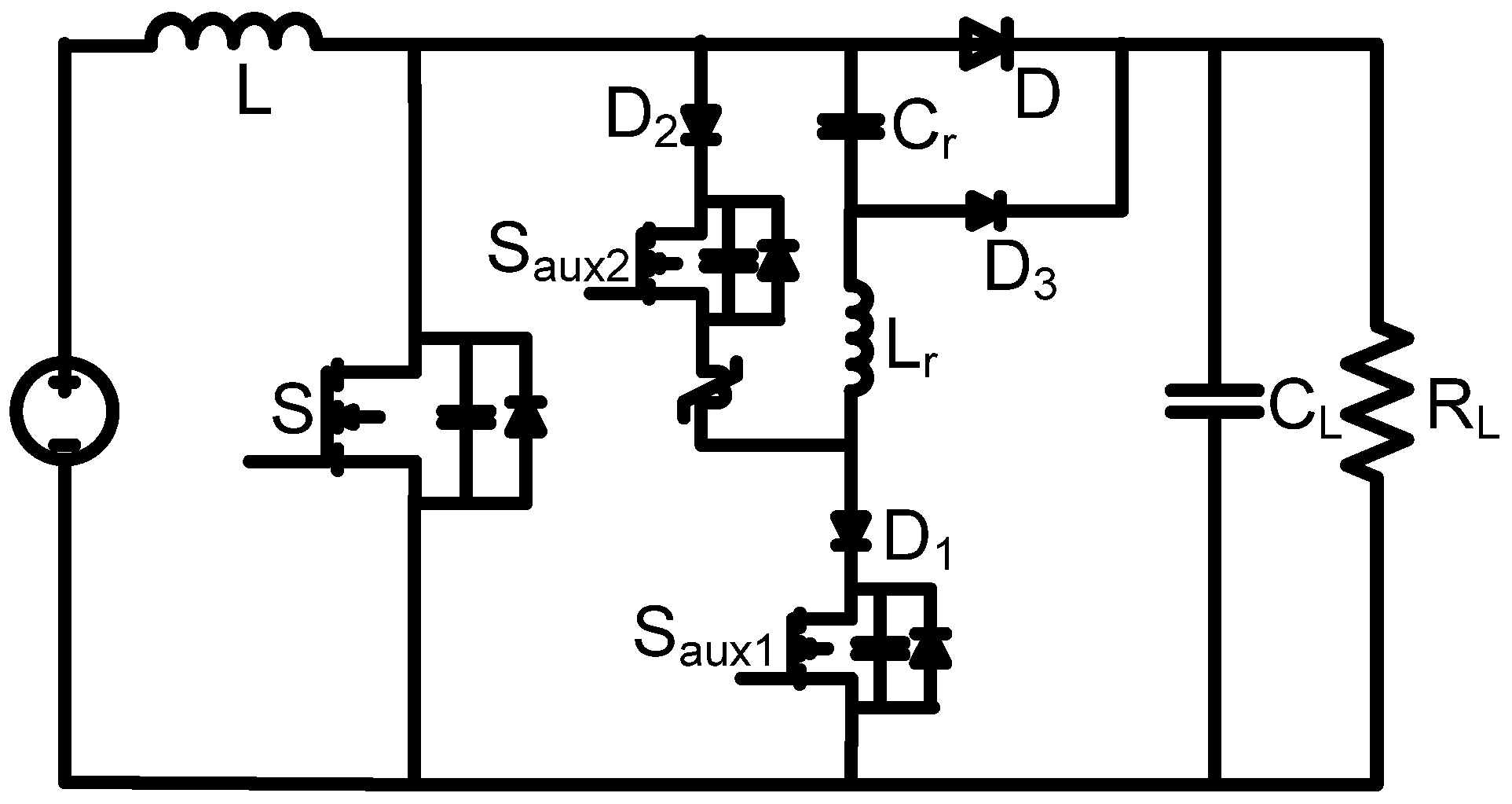
A new auxiliary circuit for ZVS-PWM converters that are implemented with paralleled MOSFETs for higher current applications is proposed in the paper. The circuit is shown in
Figure 4. Although almost all previously proposed auxiliary circuits contain only a single active switch because of cost (it is difficult to justify a two-switch circuit in a converter with a single MOSFET as the power switch), the proposed auxiliary circuit can be justified on the following grounds:
Figure 4.
Proposed DC-DC boost converter.
Figure 4.
Proposed DC-DC boost converter.
Figure 5.
(a) Three-phase six-switch rectifier. (b) Various auxiliary circuit schemes for position A. (c) Various auxiliary circuit schemes for position B.
Figure 5.
(a) Three-phase six-switch rectifier. (b) Various auxiliary circuit schemes for position A. (c) Various auxiliary circuit schemes for position B.
In the paper, the operation of the new converter is described, its steady-state operation is analyzed, and a procedure for its design is derived and then demonstrated with an example. The feasibility of the new converter is confirmed by experimental results obtained from a prototype converter.
2. Modes of Operation
The proposed converter in
Figure 4 has an auxiliary circuit that consists of two switches, S
aux1 and S
aux2, three diodes, and a resonant tank made of capacitor C
r and inductor L
r. The basic operating principles of the proposed circuit are as follows: Auxiliary switch S
aux1 is turned on just before the main power switch S is to be turned on, thus diverting current away from the main power diode D. Once current has been completely diverted away from D, the output capacitances of the switch begin to discharge and the voltage across it eventually falls to zero. The main power switch can be turned on with ZVS as soon as the capacitance is fully discharged. Due to the C
r-L
r resonant tank, the current in the auxiliary circuit naturally falls to zero, thus allowing S
aux1 to turn off with ZCS.
Sometime during the switching cycle, while the main power switch is conducting the input current, auxiliary switch S
aux2 is turned on. This action results in the voltage across C
r flipping polarity so that it is negative instead of positive. When the main power switch is turned off, the input current completely discharges C
r so that there is no voltage across it when the auxiliary circuit is reactivated sometime during the next switching cycle. Equivalent circuit diagrams of the modes of operation that the converter goes through during a switching cycle are shown in
Figure 6, and typical converter waveforms are shown in
Figure 7. To save on space, switches S
1, S
2, and S
3 are shown in
Figure 6 as a single switch, S
123.
Figure 6.
Modes of operation. (a) Model 0; (b) Model 1; (c) Model 2; (d) Model 3; (e) Model4; (f) Model 5; (g) Model 6; (h) Model 7; (i) Model 8; (j) Model 9.
Figure 6.
Modes of operation. (a) Model 0; (b) Model 1; (c) Model 2; (d) Model 3; (e) Model4; (f) Model 5; (g) Model 6; (h) Model 7; (i) Model 8; (j) Model 9.
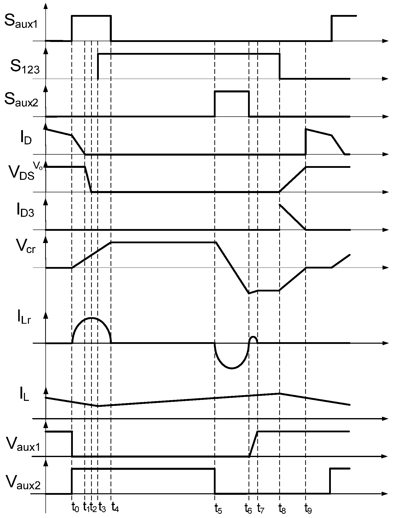
Figure 7.
Typical waveforms.
Figure 7.
Typical waveforms.
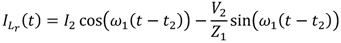
The converter’s modes of operation are as follows:
Mode 0 (t < t0): All converter switches are off during this mode and current is flowing through the main power diode D.
Mode 1 (
t0 < t < t1): At
t =
t0, switch S
aux1 is turned on and current begins to be transferred away from diode D to the auxiliary circuit. This current transfer is gradual due to the presence of inductor L
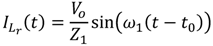
r in the auxiliary circuit, so that charge is removed at a sufficiently slow rate to allow diode D to recover; this helps minimize reverse recovery current. The equations that represent the auxiliary circuit inductor current
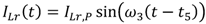
ILr and the auxiliary circuit capacitor voltage
VCr in this mode are:
where
and the initial values of
ILr and
Vcr at the beginning of this mode are zero.
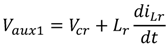
It should be noted that current can flow through the output capacitor of Saux2 after Saux1 is turned on. In order to minimize a sudden increase in current through this capacitor that can cause voltage spikes to appear, a saturable reactor or “spike-killer” inductor (Ls) should be placed in series with Saux2.
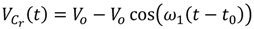
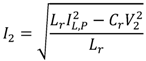
Mode 2 (
t1 < t < t2): At
t =
t1, current stops flowing through the main power diode D and the net capacitance across S
123 begins to be discharged through L
r and C
r. The current in the auxiliary circuit is the sum of the input current and the current due to the discharging of the capacitances across S
123. The equations that describe the auxiliary circuit inductor current
ILr, the voltage across S
123,
VCs, and the auxiliary circuit capacitor voltage
VCr in this mode are:
where
During this mode, the auxiliary circuit inductor current
ILr, reaches its peak when
Vc
s −
Vc
r = 0 and it is equal to the peak current of S
aux1 so that
Mode 3 (
t2 < t < t3): At
t =
t2, the capacitance across the main power switches is completely discharged and current begins to flow through the body diodes of the devices; this allows the switches to be turned on with ZVS. The equations that describe the auxiliary circuit inductor current
ILr and the auxiliary circuit capacitor voltage
VCr in this mode are:
where
Mode 4 (t3 < t < t4): At t = t3, the current that was flowing in the body diodes of the main power switches in the previous mode reverses direction and begins to flow through the switches. The modal equations of this mode are the same as those of the previous mode except that the direction of the current through the main power switches is different.
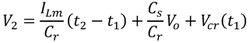
Mode 5 (t4 < t < t5): Current stops flowing in the auxiliary circuit at t = t4 due to the resonant interaction between Lr and Cr. Switch Saux1 can be turned off softly with zero-current switching (ZCS) sometime soon afterwards. The converter then operates like a standard PWM boost converter. The voltage across Cr remains fixed until Saux2 is turned on later in the switching cycle.
Mode 6 (
t5 < t < t6): At
t =
t5, auxiliary switch S
aux2 is turned on, sometime before the main power switches are turned off. As a result, capacitor C
r begins to discharge through L
r, S
aux2 and D
2, and the voltage that was across it at the start of the mode changes polarity. At the end of this mode, the current in C
r and L
r is zero so that S
aux2 can be turned off with ZCS. The equations that define this mode are:
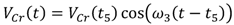
Mode 7 (
t6 < t < t7): The output capacitance of S
aux1 needs to be charged after this switch has been turned off so that current continues to flow through L
r and C
r. The length of this mode is negligible compared to the length of the other modes given that the output capacitance of S
aux1 is much smaller than C
r, but the voltage across C
r can be changed during this mode. The voltage across S
aux1 during this mode can be expressed as
where
It should be mentioned that if the output capacitance of Saux1 is charged to less than the output voltage Vo during this mode, then it would be charged up to Vo during Mode 9 when the main power switches turn off.
Mode 8 (t7 < t < t8): During this mode, the main power switches are still on and current in the input inductor rises.
Mode 9 (
t8 < t < t9): At
t =
t8, the main power switches are all turned off. The voltage of the net capacitance across the main power switches is
As a result, the auxiliary circuit capacitor Cr begins to be discharged as the net capacitance across the main switches continues to be charged; the energy stored in Cr is transferred to the output during this mode. The mode ends at t = t9 and the converter enters Mode 0, where it remains until Saux1 is turned on.
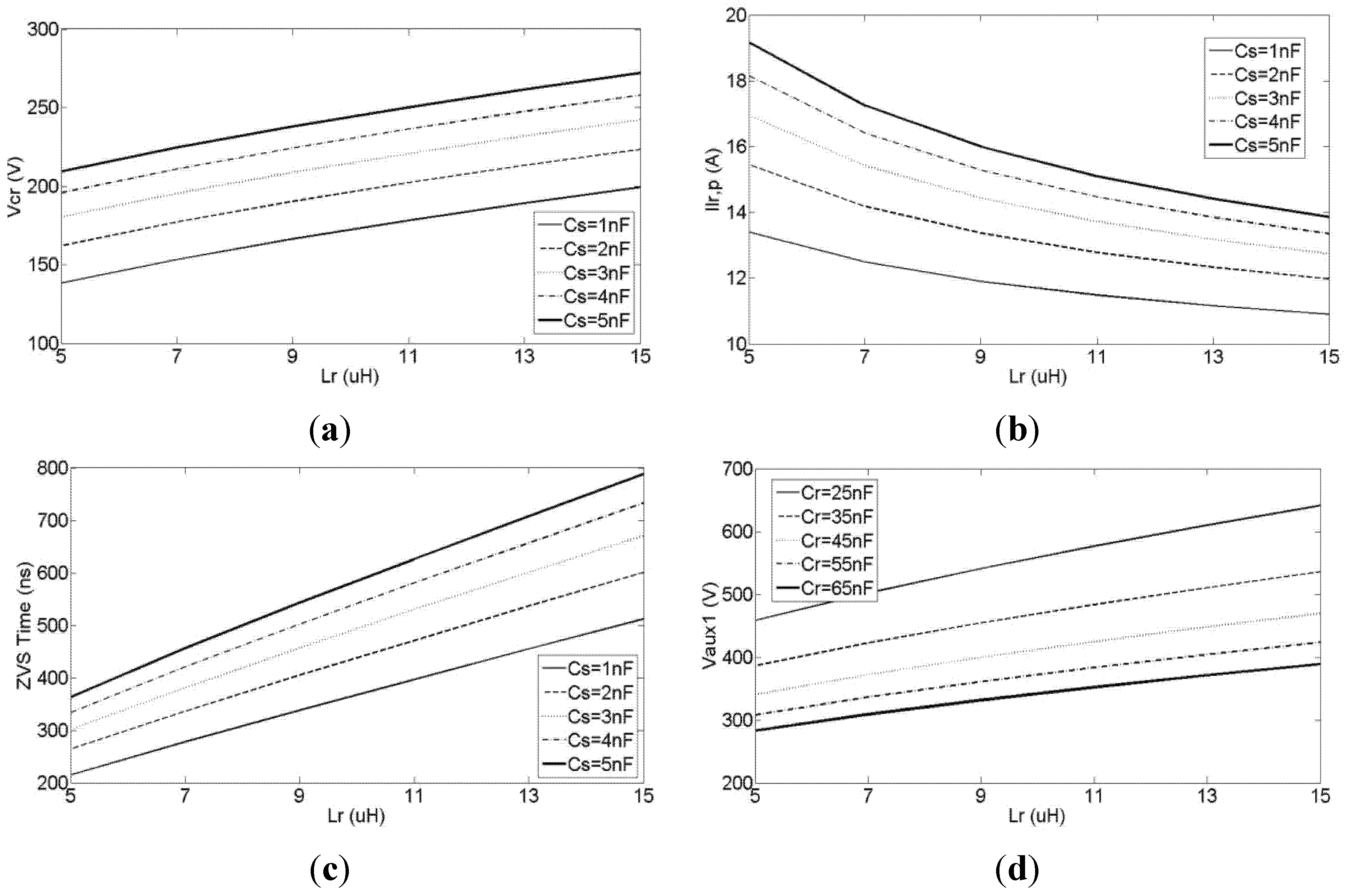
3. Steady-State Characteristics
The modal equations that are derived in the previous section of the paper can be used to generate steady-state characteristic curves that can be used to see the effect of certain key parameters on the operation of the auxiliary circuit. These key parameters include the values of auxiliary circuit components L
r and C
r and the net capacitance across the main power switches, C
S. Examples of such graphs are shown in
Figure 8. Each graph has been generated by keeping certain parameters constant, then varying other parameters to see the effect of doing so.
Figure 8.
Characteristic curves. (a) Graph of characteristic curves of Vcr vs. Lr for different values of CS with Cr = 50 nF; (b) Graph of characteristic curves of ILr vs. Lr for different values of CS with Cr = 50 nF; (c) Graph of characteristic curves of ILr vs. Lr for different values of CS with Cr = 50 nF; (d) Graph of characteristic curves of Vaux1 vs. Lr for different values of Cr with CS = 2 nF.
Figure 8a is a graph of
Vcr vs. Lr for different values of
CS with
Cr = 50 nF. This graph shows that
Vcr increases as either
CS or
Lr is increased. The first characteristic can be explained by noting that increasing
CS increases the amount of energy that is discharged into the auxiliary circuit and is stored in
Cr after the main power diode stops conducting. More energy in
Cr results in higher values of
Vcr. On the other hand, according to (4) and (12), higher values of
Lr increase the time duration between
t0 and
t2; therefore, more energy is transferred to
Cr, which leads to higher values of
Vcr.
Figure 8b is a graph of characteristic curves of
ILr vs. Lr for different values of
CS with
Cr = 50 nF. This graph shows that when
CS increases, more energy is stored in
Cr, which results in higher peak values for
ILr. Moreover, when
Lr increases, it extends the resonant cycle and reduces the peak value of
ILr. The average value of the resonant current is related to
CS and load current and is independent of length of the resonant cycle and the peak of the resonant current.
Figure 8c shows a graph of characteristic curves of ZVS time values
vs. Lr for different values of
CS with
Cr = 50 nF. These time values are when the net capacitance across the main power switches is completely discharged after S
aux1 is turned on and is measured from the turn-on instant of this switch. The graph shows that the ZVS times increase as
Lr or
Cr increases. Increasing
Lr increases the time needed for current to be transferred away from the main power diode and it also increases the resonant cycle of the auxiliary circuit. On the other hand, by increasing
CS, the amount of stored energy in this capacitor increases and, therefore, it takes more time for it to be discharged.
Figure 8d shows a graph of characteristic curves of
Vaux1 vs. Lr for different values of
Cr when
CS = 2 nF. It can be seen that increasing
Lr increases the maximum voltage across S
aux1. Before D
1 goes off after Mode 7 and
Vaux1 becomes constant,
Vaux1 is
Equation (26) shows that Vaux1 is increased by increasing Lr. Also, for the same amount of energy transferred to Cr, increasing Cr reduces the voltage across it and thus reduces Vaux1 as well.
5. Variations of the Auxiliary Circuit
The basic structure of the new auxiliary circuit can be modified in several ways, either to improve performance or to reduce cost. Several of these modified circuits are shown in
Figure 9.
Figure 9.
Modified structures of new aux circuit.
Figure 9.
Modified structures of new aux circuit.
The circuit shown in
Figure 9a is an auxiliary circuit that has a different resonant inductance when auxiliary switch S
aux2 is conducting current than when S
aux1 is conducting current. Having the resonant inductance be different under these two sets of circumstances allows the resonant inductance to be tailored to achieve the best performance for each set of circumstances.
The circuits shown in
Figure 9b,c are auxiliary circuits with transformers in them. The presence of a transformer in the auxiliary circuit helps reduce circulating current losses after S
aux2 has been turned on. The transformer allows energy to be transferred from the auxiliary circuit to the load instead of it just being trapped in the auxiliary circuit, where is contributes to losses. Moreover, the presence of a transformer in the auxiliary circuit makes the design of this circuit more flexible as it provides an additional degree of freedom.
The circuit shown in
Figure 9d is a simplified version of the basic auxiliary circuit. The circuit has been simplified by
Figure 4. What this does is to make current continuously flow in the auxiliary circuit inductor. Since this can happen, auxiliary circuit conduction losses may increase. This circuit variation can be considered for lower currents if it is desired to save on the cost of two diodes.
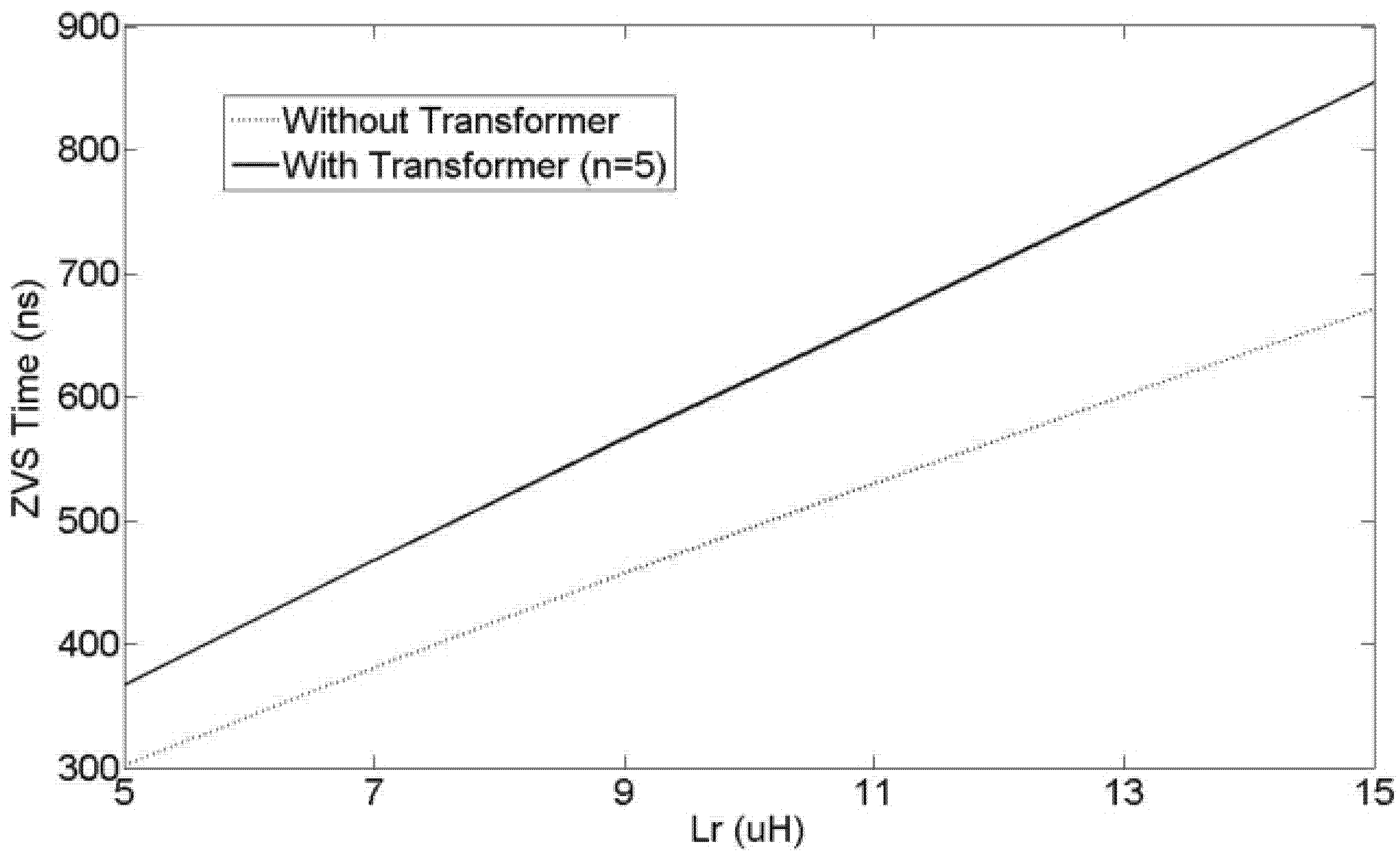
Figure 10 shows a graph of ZVS time interval
vs. auxiliary circuit inductor value for the basic auxiliary and for the circuit in
Figure 9c, implemented with an auxiliary circuit transformer turns ratio of
n =
N2/
N1 = 5. It can be seen that implementing the auxiliary circuit with a transformer can result in extending the amount of time that is available for the main converter switches to turn on with ZVS. This allows for greater flexibility in the design and the performance of the converter.
Figure 10.
Graph of characteristic curves of ZVS time values vs. Lr for different values of n with Cr = 50 nF and Cs = 3 nF.
Figure 10.
Graph of characteristic curves of ZVS time values vs. Lr for different values of n with Cr = 50 nF and Cs = 3 nF.
6. Experimental Results
An experimental proof-of-concept prototype of the proposed converter was built to confirm its feasibility. The converter was built according to the same specifications as in the design example with input voltage Vin = 70 V, output Vo = 375 V, maximum output power Po,max = 700 W and switching frequency fsw = 100 kHz. The main power boost circuit was implemented as described in the design example. IRFP840 MOSFETs were used for the two auxiliary switches and 15ETX06 diodes for diodes D1, D2, D3. The values of Lr and Cr were Lr = 8.2 μH and Cr = 44 nF.
Typical experimental waveforms are shown in
Figure 11.
Figure 11a,b shows the current waveform of
Lr,
ILr, and the gating signals of the two auxiliary switches. Since the positive part of
ILr and the negative part of
ILr represent the currents through S
aux1 and S
aux2 respectively, it can be seen that both switches can be turned off softly with ZCS.
Figure 11c shows the gating signal and the drain source voltage of a main power switch. It can be seen that the switch turns on with ZVS, as the voltage across the switch is zero before it is turned on.
Figure 11d shows the auxiliary inductor current and capacitor voltage waveforms. It can be seen that whatever energy is placed in C
r is removed before the auxiliary circuit is reactivated.
Figure 11.
Experimental waveforms. (a) Upper Signal: Gating signal VGS of Saux1 (V = 20 V/div.) Lower Signal: Current of Lr resonant inductor (I = 5A/div.) Time: t = 2.5 μs/div. (b) Upper Signal: Current of Lr (I = 5 A/div.) Lower Signal: Gating signal VGS of Saux2 (V = 10 V/div.) Time: t = 2.5 μs/div. (c) Upper Signal: VGS of main switch (V = 10 V/div.) Middle Signal: Current of Lr (I = 5 A/div.) Lower Signal: VDS of main switch (V = 200 V/div.) Time: t = 2.5 μs/div. (d) Upper Signal: Current of Lr (I = 5 A/div.) Lower Signal: Voltage of Cr (V = 100 V/div.) Time: t = 2.5 μs/div.
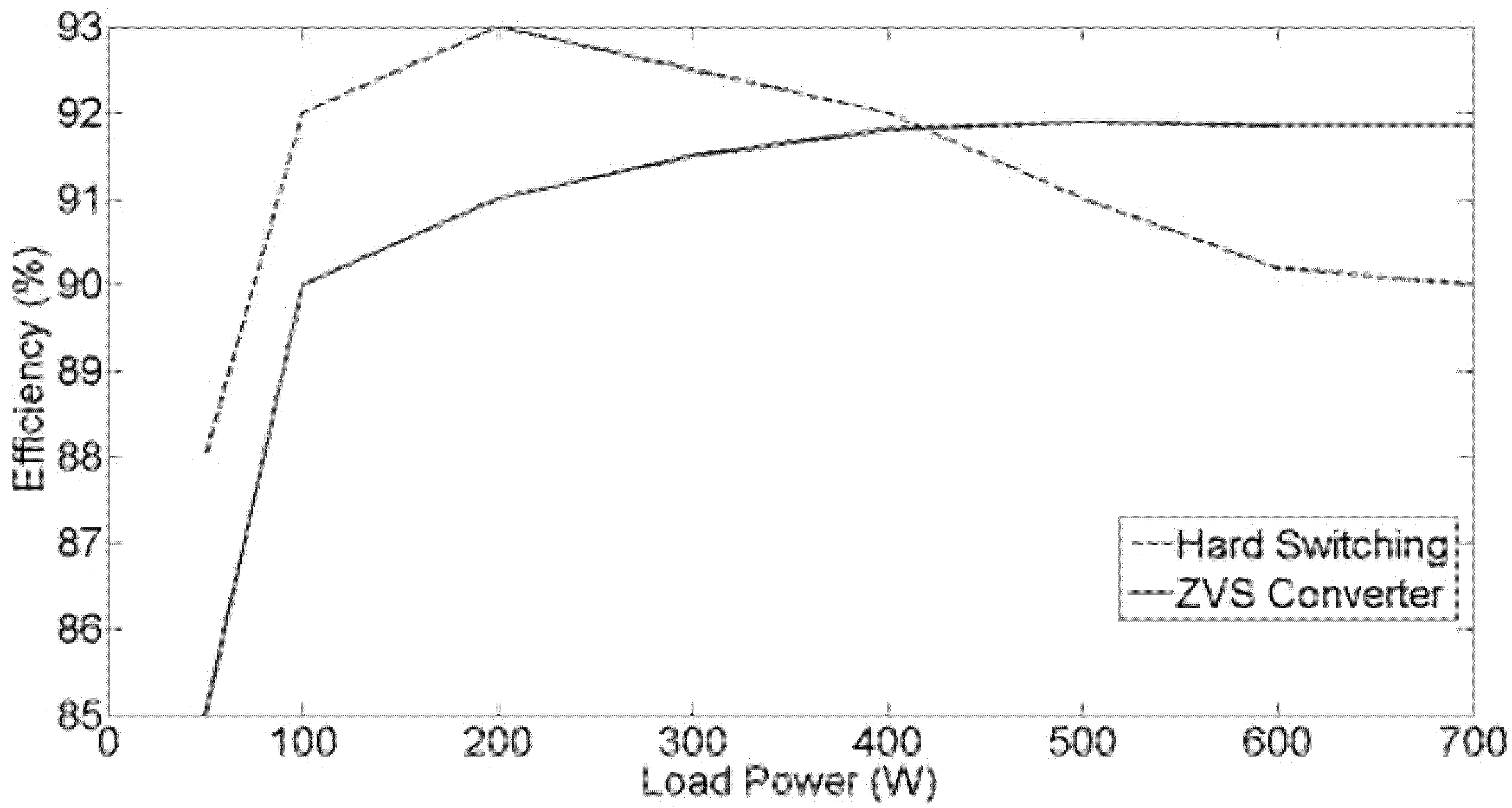
Figure 12 shows a graph of converter efficiency
vs. load for the cases of the prototype with and without the basic auxiliary circuit. It can be seen that the converter efficiency dips sharply when the converter is operating with a heavy load while this does not happen when the converter has the basic auxiliary circuit. The comparison was limited to 700 W as the efficiency of the hard-switched converter becomes very poor past this point, while this is not the case for the ZVS converter. The reason for the sharp fall off in efficiency is the fact that the converter was operated with a high input current—higher than what is normally considered for a boost converter [
15]. High current boost applications can include boost converters for solar power systems and telecom systems.
For the low power range, the efficiency of the hard switching circuit is better because there is relatively little current in the circuit so that turn-on switching losses, which depend on the product of switch voltage and current during switch turn-on, are low. Moreover, the hard-switching converter does not have any losses that are caused by an auxiliary circuit, which consumes some energy. When the load is low, the energy saved by the auxiliary circuit is less than its consumption. For the high power range, the turn-on losses for the hard-switching converter become very high and are greater than the power consumed by the auxiliary circuit of the soft-switching converter, which has ZVS, so that the soft-switching converter is more efficient.
Figure 12.
Efficiency vs. load power.
Figure 12.
Efficiency vs. load power.


