

Active Disturbance Rejection Control of Full-Bridge DC–DC Converter for a Pulse Power Supply with Controllable Charging Time
College of New Energy, China University of Petroleum (East China), Qingdao 266580, China
*
Author to whom correspondence should be addressed.
Electronics 2023, 12(24), 5018; https://doi.org/10.3390/electronics12245018
Submission received: 6 November 2023
/
Revised: 30 November 2023
/
Accepted: 7 December 2023
/
Published: 15 December 2023
(This article belongs to the Special Issue Advances in Pulsed-Power and High-Power Electronics)
Abstract
:In this paper, a control method of a full-bridge DC–DC converter for a pulse power supply with controllable charging time based on Active Disturbance Rejection Control (ADRC) is presented. For this application, the scheme objective is to achieve a flexible charging current to adjust the charging time of the pulse power supply. Due to the existence of switching devices in the system, the dynamic characteristics of the control system are complicated; an LADRC (Linear Active Disturbance Rejection Control) controller is constructed to regulate the charging of the converter current so as to improve the flexibility and dynamic performance of high-voltage pulse power supply. LADRC linearizes the extended state observer and links its parameters to the observer bandwidth to simplify the design of ESO. The proportional coefficient or differential coefficient is connected with the bandwidth of the controller to simplify its tuning, simplify the nonlinear function, more parameters, and complicated adjustment of the ADRC in practical application. The inner loop current regulator assembled is beneficial to the dynamic performance of the loop. The resulting double closed-loop structure improves steady-state and transient current-tracking performance. In addition, stability analysis of the proposed strategy is also performed. The proposed control approach is compared with PI. To verify the feasibility of the proposed scheme, an experimental prototype was constructed and tested to confirm the superiority of the proposed method in terms of dynamic performance.
1. Introduction
Rapidly releasing the stored energy into a load in the form of electrical pulses can generate large amounts of instantaneous power over a short period; this strategy is called pulse power [1]. The pulse power supply that delivers such pulse power is called pulse power supply, which has been conducted in various works in the field of pulse power and has a very wide range of applications in industry. At present, the pulse power supply is devoted to food processing, medical treatment, water treatment, exhaust gas treatment, ozone generation, engine ignition, ion implantation, and others [2]. For instance, a high-voltage pulse generator for water treatment was introduced in Ref. [3], Ref. [4] presented the effect of a pulsed electric field on inducing apoptosis of cancer cells, and Ref. [5] designed a pulse power supply system with a special structure to develop the technology required for inertial fusion power plants. In addition, the emergence of new silicon carbide devices has improved the application range and performance of pulse power supplies [6,7,8,9,10]. Therefore, pulse power supply technology is in possession of great potential for development.
In general, a pulse power supply is composed of single capacitor charging and discharging circuits, magnetic pulse compressors, pulse-forming networks, multistage Blumlein lines, and Marx generators. This structure is mostly classified under the voltage source topology category [1] and suffers from drawbacks such as the imbalance of control output voltage level and stress and the inflexibility of power transmission to the load, which could lead to the system having problems such as insufficient efficiency and flexibility. With the development of power semiconductor devices, advanced pulse generation techniques were brought from the emergence of modern power electronic switches, such as full-bridge, half-bridge, push–pull, forward, and flyback converters in hard-switching or resonant topologies [11]. These power semiconductor structures have inherent operational flexibility and can extend the pulse-power capability to other circuits. There are many DC–DC power converters as a means to provide high output voltage. [12] installed DC–DC converters in pulse power supply, and [13,14,15] displayed the asset of using DC–DC converters in pulse power supply applications. Among the above DC–DC power supply topologies, the full-bridge DC–DC converter is a widely accepted topology for the medium to high power range, which offers many advantages, for example, the voltage and current stress of the switch are relatively low, the switch voltage stress does not exceed the DC voltage, the equal use of all switches, the achievement of high-power density, and the flexibility of the control scheme [16]. Therefore, the use of a full-bridge DC–DC converter in the pulse power supply is very attractive. In addition, in order to increase the flexibility of the pulse power converter, ref. [14] proposed a topology using the concept of the current source, which is connected to the inductor through a switch as a current source, and adjusts the energy stored in the current source by changing the current size, pumping the inductor current into the capacitor to charge the capacitor and generate high voltage and high pulse power on the load, thus significantly improving the efficiency of various systems with different requirements, making the pulse power converter very flexible in terms of energy control. Therefore, taking a full-bridge DC–DC converter as the topology of pulse power supply and adding the concept of the current source, a topology of pulse power supply with a controllable charging current based on a full-bridge DC–DC converter is proposed.
However, the control design of a full-bridge DC–DC converter submits several challenges. First, the switching devices in the converter have very complex time-varying switching behavior, which determines the shape of the inductor current, making it difficult to establish a dynamic model of the power converter. Next, the converters used in pulsed power systems have a wide range of operating conditions, and the charging time is also very sensitive to disturbances, which complicates the control design. Furthermore, the control input range is limited due to the physical limitations of the power converter [17]. Therefore, in view of the above problems, the classical PI (Proportional Integral) control strategy may have difficulty meeting the performance requirements of the system due to its slow dynamic response speed and sensitivity to disturbances [18], and the required high performance may exceed the capacity of the PI controller in the variation of working conditions or system parameter changes [19]. With the development of advanced control theory and the improvement of the computing power of microprocessors, it is possible to use advanced control algorithms to meet the high-performance control requirements of the system. There are many advanced control methods for H-bridge converter circuits, such as hysteresis control [20,21], model predictive control (MPC) [22,23], and sliding mode control (SMC) [24,25]. Among the above control strategies, hysteresis control has the advantages of simple algorithm implementation, fast response, and strong robustness to disturbances, but it also has disadvantages such as variable switching frequency and high-frequency tremor [23]. Model predictive control can predict future control vectors to optimize a certain cost function, making the control of this cost variable reach the fastest control without regard to accurate prediction requiring high computational costs, which may limit its application in practical engineering [17]. For sliding mode control, since disturbances usually vary over a large range, the robustness of sliding mode control to disturbances is usually achieved using higher switching gains, which can create undesirable chattering problems [26].
In this paper, the control of a full-bridge DC–DC converter for a pulsed power supply with a controllable charging time based on the ADRC (Active Disturbance Rejection Control) theory is proposed to improve the robustness ability and dynamic performance of the system. At the beginning of the design controller, according to the proposed topology of the converter pulse power supply, a mathematical model is established. Conforming to the mathematical model, the unmodeled model parameters and coupling variables of the full-bridge DC–DC converter are regarded as system disturbances and a linear extended state observer is established. Then, a linear active disturbance rejection controller is designed to control the charging current of the pulse power supply.
The rest of this paper is organized as follows: In Section 2, the topology of a pulsed power supply with a full-bridge DC–DC converter structure will be introduced and its operation will be analyzed. Section 3 is devoted to the mathematical models of the pulsed power supply and the full-bridge DC–DC converter and building the control structure. Section 4 focuses on the design of ADRC controllers and shows the analysis of stability. Simulation waveform results and experimental results will be presented in Section 5. The conclusions are then given in Section 6.
2. Topology and Operation Principle
2.1. Topology
The topology of the proposed pulse power supply with a controllable charging time in this paper is illustrated in Figure 1. The topology consists primarily of a full-bridge converter, which is composed of four insulated gate bipolar transistors (IGBT) and a high-frequency transformer, as well as a full-bridge uncontrolled rectifier circuit, an air gap switch, and multiple inductors and capacitors.
In the circuit shown in Figure 1, is the load. is the internal resistance of the inductor , which incorporates the junction inductance of the circuit line between the input and inverter. is equivalent to the internal resistance of the smooth inductor and the resistance of the circuit. The equivalent circuit model of the high-frequency transformer that can be simplified as an ideal transformer with a primary series inductor , which is the leakage inductance of the high-frequency transformer from the primary side, is T in Figure 1, where the “” represents the dotted terminals of the transformer T. and are the body diode and snubber capacitors of the IGBT (Insulated Gate Bipolar Transistor), respectively. is the energy storage capacitor, which releases the stored energy to the load through the air gap switch .
2.2. Operation Principle
In order to facilitate the analysis of the operation principle of the full-bridge DC–DC converter for pulse power supply, it can be described in parts and the following assumptions can be made:
- All components are considered ideal;
- Input voltage is a constant;
- Regardless of the transformer saturation effect.
As shown in Figure 1, Voltage provides the DC input for the pulse power supply, and after passing through the filter capacitor C and the inductor , it provides the input for the full-bridge converter. The modulation method of a full-bridge DC–DC converter is usually phase-shift modulation [27,28,29], but in view of the difference of the control purpose, the full-bridge DC–DC converter adopts the sine pulse width modulation (SPWM). Through this modulation strategy, the four IGBT switches of the full-bridge DC–DC converter are controlled to transfer corresponding energy to the high-frequency transformer. Specifically, the modulation mode of SPWM (Sinusoidal Pulse Width Modulation) is unipolar sinusoidal pulse width modulation. Unipolar SPWM is a modulation method in which the carrier is positive and the output voltage is positive in the positive half period of the modulated sine wave, and the carrier is negative and the output voltage is negative in the negative half period of the modulated sine wave, and the signal generated by the crossover of the modulated wave and the carrier is used to drive the diagonal switching tube.
In the USPWM (Unipolar Sinusoidal Pulse Width Modulation) process, the carrier and modulation wave are represented by and , and the action waveforms of the four switches of the full-bridge converter are shown in Figure 2. The operating stages of the full-bridge DC–DC converter when USPWM is used are as follows. Under stable operation, the switching waveform and operating circuit during the switch cycle are shown in Figure 3 and Figure 4.
- Interval 1 ( − )
During interval 1, the operating state of the IGBT switching device in the H-bridge is shown in Figure 3a. The current flows through the main switches , transformer leakage inductor , transformer primary, and . The voltage across the stray inductor is tended to and the slope of its current is:
Equation (1) ignores the influence of stray components.
- Interval 2 ()
Operating in interval 2, the operating state of the IGBT switching device in the H-bridge is shown in Figure 3b. The main switches and turn off. The voltage is tended to by switches and turning on. The slope of the current is:
Figure 4 shows the operating waveform of the full-bridge DC–DC converter when operating in interval 1 and interval 2. As can be seen in Figure 4, when the H-bridge converter circuit operates in interval 1, the current flowing through the primary side of the transformer will increase in a positive direction; when the H-bridge converter circuit operates in interval 2, the current flowing through the primary side of the transformer will increase in a negative direction. Therefore, the duty cycle of the switching tube of IGBT can be controlled to adjust the current , to control the charging current of the pulse power supply.
After the above modulation process, the high-frequency transformer transfers the power to the full-bridge uncontrolled rectifier circuit. The operation modes of this topology are classified into the following two separate parts: the supplying part and the discharging part.
For the pulse formation portion, the proposed circuit diagram includes a rectifier bridge that is connected to the converter, and an inductor is connected to it as a current source. A capacitor that is connected to the current source can generate a high-voltage pulse, which is the energy supplied by the controller that controls the current through the inductor.
- Supplying Stage
To simulate the behavior of the pulse power supply, a simple resistance model with an air switch is chosen to simulate the charge–discharge process. The general concept of pulse is based on the transfer of energy stored in a capacitor to the load. To achieve this condition, inductive current should be pumped into the capacitor to charge the capacitor and generate a high voltage over the entire load.
The rectified current flows through the inductor for filtering and remains at a fixed value after sampling control. At this time, the switch is disconnected. The current maintains a certain value to charge the capacitor . During this time, the charge flowing through the inductor is equal to the amount of charge accumulated on the capacitor , and the relationship between the two is defined by (3):
Under a certain charging current, after setting the output voltage , the charging time t can be calculated by (4):
- Discharging Stage
For the discharging process, since the value of the capacitor is smaller in comparison with the inductor, the energy stored in the capacitor will be released by the air gap switch faster than the inductor. In addition, a high current will be generated for a short period of time with the release of energy from the capacitor to the load. When the voltage on the load drops to a certain value, the switch is turned off to charge the capacitor with a constant current. Then, the supply and discharge process can be repeated. The operation circuit of the supplying stage and discharging stage is shown in Figure 5a,b, respectively.
According to Figure 5b, this is a typical first-order zero-input response, so the voltage on the load and the current flowing through the load are
From the above expression (5), it can be seen that the voltage and current on the load decay exponentially due to the small capacitance value, the time constant is large, and the decay rate is fast, with a time constant of .
The operation mode of the pulse power supply with this topology can control the charging time with (4), making the pulse power converter very flexible in terms of energy control.
3. System Structure
At present, a voltage-controlled pulse power supply system is often used in pulse power technology, and the charging current of the voltage-controlled pulse power supply system is nonlinear in the charging process of the energy storage capacitor, which makes the charging time non-linear, and it is difficult to control the discharge frequency target. The current control strategy can achieve an adjustable charging current and linear controllable charging time, which is convenient to gain control of the discharge frequency target. The current control circuit can reduce the influence of the transient short circuit of capacitive load on the circuit and improve the reliability of the pulse power supply.
To accomplish the above functions of the proposed pulse power supply, the full-bridge DC–DC converter needs to be controlled, so it is necessary to establish a mathematical model of the pulse power supply system to facilitate the design of the control structure. For the establishment of the dynamic model, the following assumptions are made: the input voltage is constant, both the high-frequency transformer and the inductance are linear, and saturation is not considered. In combination with the topology shown in Figure 1, the dynamic model of this pulsed power supply system can be expressed as
where is the reciprocal of the transformation ratio of the high-frequency transformer; is the output of the primary side of the transformer, where is the switch function with values of 1, 0, and −1.
By Equation (4), it can be seen from the previous analysis that the charging time of the pulse power supply is controllable, which keeps the current on the inductor constant. Therefore, a current feedback control structure can be designed.
A current double closed-loop control structure is presented here. Utilizing this control strategy combined with the dynamic model established by (6), the control system of the pulse power supply is shown in Figure 6.
The outer loop is a direct current control loop, and the output of the outer loop regulator is the command of the inductor current at the input side of the full-bridge converter; its purpose is to require the input and output side inductor currents tracking command current. This kind of current inner-loop control, because the current regulator is set in its structure, not only achieves the tracking and adjustment of the inductor current on the input side but also transforms the control object of the current outer loop, thereby improving the dynamic performance of current outer-loop control system.
4. ADRC-Based Current Control
The application of PI controllers is a challenging problem for the control of the charging current of the pulse power supply system. Firstly, the complex switch behavior of the power devices of the full-bridge DC–DC converter makes it difficult to establish an accurate dynamic model, and this behavior directly acts on the charging current, which brings a series of uncertain factors. Secondly, the charging time of the pulse power system is also very sensitive to disturbance, which will increase the difficulty of control. In addition, there is the dead time effect of SPWM. From the above control point of view, it can be concluded that the robustness to parameter changes and disturbances must be a key attribute in the control. These high-performance requirements may exceed the capabilities of the PI controller. Therefore, a charging current control strategy based on ADRC is proposed to replace PI control to treat the unmodeled uncertainty as part of the disturbance and estimate and compensate for the impact of the disturbance in the controller, which ensures good tracking of charging current reference and robust stability to parameter changes and disturbances, so as to improve the performance of outer loop control.
4.1. Formation of ADRC-Based Current Controller
In the framework of ADRC, combined with the control structure of Figure 6, Equations (4) and (6) can be reformulated to obtain (7):
Making the assumption that the precise mathematical model of the system is unknown and considering the external disturbance , the system dynamics can be reformulated in the ADRC framework as
where is the output signal of the system; is the controller input signal; is the output-related model of the system, in which the functional relationship can be partially known, unknown, linear, or nonlinear; is a system parameter, in which the functional relationship can be partially known, unknown, linear or nonlinear; is the total disturbance of the system, including internal disturbance and external disturbance.
In the ADRC framework, the output signal of the system is defined as state , and the perturbations related to system parameters and disturbance are defined as the extended state . Assuming that and are differentiable, the system dynamics (8) can be defined in the state space:
The corresponding linear extended state observer can be designed as follows:
where is the state variable of the extended state observer and is the gain of the observer. By selecting the appropriate observer gain, the observer can track each variable of the system.
Formula (10) can be reformulated and expressed in the following matrix form:
where is the estimate of the state variable and , and is the observer gain vector.
In Formula (11), matrix , , , and are, respectively,
The bandwidth parametrization method for observer gain vector is usually designed as follows:
where is the identity matrix.
According to Equation (13), the relationship between observer gain and bandwidth can be obtained:
where is the bandwidth of LESO (Linear Extended State Observer) whose value is greater than zero.
For the above system, the estimated variables can be used to implement the control law, including the disturbance rejection and feedback control law, and the equation of the designed controller is
where is the input signal, is the control error, is the gain of the controller, is the amount of control before compensation, is the estimated total disturbance, and parameter is the “compensation factor” that determines the strength of the compensation, which is used as an adjustable parameter.
Then, combining Equations (10) and (15), the transfer function of the closed-loop control when the disturbance is compensated is given by
The popular bandwidth parameter method for controllers is to assign the poles to the left half of the real axis of the S-plane so that controller gain can be determined:
where is the bandwidth of the controller whose value is less than the bandwidth of the LESO.
In summary, the LESO and the control law above constitute an ADRC control, which takes the following form:
The block diagram of the active disturbance rejection control structure is shown in Figure 7.
In Figure 7, is the input reference current instruction, and the control instruction can be obtained by the designed LADRC (Linear Active Disturbance Rejection Control) control law. is the input reference instruction of the inner loop, passes through the inner loop PI controller (not given in Figure 7, which can be regarded as contained by the input disturbance ), and according to the mathematical model of Equation (7), The output value of the outer loop controller can be obtained, and the actual output can be obtained by superimposing the measurement noise . can finally track the input instruction by continuously correcting the error through the LESO at the bottom of Figure 7. Thus, after the charging current is tracked, the charging time can be changed according to Formula (4).
4.2. Stability Analysis
To analyze the stability of the designed controller, it is generally necessary to establish an expression of the transfer function for the control system in the frequency domain whose function is to analyze the frequency domain characteristics of the system. However, the transfer function of the active disturbance rejection controller cannot be directly obtained [30,31], which is derived below.
By Laplace transformation of Equation (10),
Perform Laplace transformation on Equation (15) and substitute Equation (19) to obtain,
where
The outer-loop control of the ADRC control of the system can be regarded as the controller and the prefilter in series, as shown in Figure 8. The control law (20) and Figure 8 imply that the ADRC-based current control scheme is equivalent to a 2DOF (Two Degrees of Freedom) control structure.
In the ADRC transfer function block diagram shown in Figure 8, ADRC serves as the control outer loop, and the inner loop is decoupled by PI control, so the transfer function of the plant is
According to Figure 8, and combining Equations (20)–(22), it can be concluded that the outer-loop closed-loop transfer function of the ADRC controller of the system is as follows:
The ADRC-based current controlled system depicted in Figure 8, with equivalent transformation depicted in Equation (23). The characteristic polynomial of the closed-loop system represented by Equation (23) is as follows:
where
The Full-Bridge DC–DC Converter for a Pulse Power Supply system parameters used in the design case is given in Table 1. Changing the bandwidth of the controller and the observer can change the open-loop gain of the system shown in Figure 8, thus affecting the stability of the system. Figure 9a,b show that by changing the controller and observer bandwidth, the stability margin is changed. Obviously, the stability of the system depends on the controller bandwidth and the observer bandwidth.
In practice, the observer bandwidth usually chooses an appropriate value to seek a compromise between the speed of state estimation and noise sensitivity, while the control bandwidth is chosen according to a desired settling time.
When using the designed controller parameters shown in Table 1, applying the Hurwitz criterion to Equation (24) yields:
It is shown that the proposed control strategy is stable for the designed parameters.
5. Simulation Results and Experimental Verification
5.1. Simulation Results
To evaluate the performance of the proposed LADRC-based control method with the designed system and controller parameters listed in Table 1 (in the simulation, the load is 10 Ω. Since the discharge period is much shorter than the charging period, only the marking of the charging period is given in the following simulation figures), simulations have been carried out in the MATLAB/Simulink environment based on the system shown in Figure 6 and the current controller shown in Figure 7.
5.1.1. Steady-State Performance
The simulation results of the pulse power supply under the proposed LADRC-based control method are shown in Figure 10a. As can be seen, the proposed control strategy is capable of tracking the charge current so that the charging time of the pulse power supply can be controlled.
The steady-state charging current is set to 2 A as shown in Figure 10a. When the discharge voltage of the pulse power supply is set to 3000 V, due to the shorter discharge time compared to the charging time, the charging and discharging period can be obtained as 0.015 s according to Equation (4), and the voltage waveform on the capacitor is shown in Figure 10b.
5.1.2. Robustness under Parameter Variations
The effectiveness of the LADRC-based control under parameter variations is compared with the PI control. Two transformers with leakage inductances of 5 μH and 3 μH are set up in the simulation, and their inputs are connected to the system by an ideal switch. Firstly, the transformer with a leakage inductance of 5 μH is connected to the system. At 0.3 s, a switch signal is sent to the switch control port to disconnect the transformer with a leakage inductance of 5 μH from the system, and the transformer with a leakage inductance of 3 μH is connected to the system. The above simulation settings are used to test the robustness of the system under parameter changes. Simulation results are shown in Figure 11 and Figure 12. As shown in Figure 11a, when the leakage inductance of the transformer is decreased from 5 μH to 3 μH at 0.3 s, the PI-based control system loses its stability due to leakage inductance varying too much. The undesirable effect of the parameter variation can be mitigated by the ADRC as shown in Figure 12a. The proposed method provides a stable system performance even after sudden variations of the leakage inductance of the transformer, which means that the proposed control has the advantage of adaptability for the operation environment. Thus, the ADRC control offers a superior feature in comparison with PI control.
As shown in Figure 11b, the system based on PI control loses stability due to the change in leakage inductance parameters at 0.3 s, and the voltage waveform of the energy storage capacitor is not desired. Figure 12 shows the control system based on ADRC is slightly affected, but it can maintain the overall stability of the system, and the voltage waveform of the energy storage capacitor meets expectations.
5.1.3. Transient Performance
To compare the transient response performance of the current under the PI controller and the ADRC controller, Figure 13a,b show the step-down response and step-up response of the charging current when the current reference changes from 2.5 A to 2 A and from 2 A to 2.5 A, respectively. It is found that compared with PI control, the proposed control method has a good charging current reference tracking ability, a good dynamic performance, and a fast transient response. The period of the output voltage also changes accurately in the corresponding current.
5.1.4. Anti-Disturbance Performance
The anti-disturbance performance of the proposed method in the system is tested by appropriately changing the size of the input voltage , and the simulation results are shown in Figure 14. Under the condition of 2 A charging current, the input voltage is reduced from 300 V to 150 V at 0.3 s. As can be seen from Figure 14, when the input voltage is reduced at 0.3 s as a disturbance signal, the charging current under PI control is slightly affected by this disturbance and recovers the state before the disturbance after 0.3 s. The proposed method is not affected by the same degree of disturbance. It can be seen that the ADRC used has a stronger anti-interference ability than the PI control.
5.2. Experimental Results
A laboratory prototype has been built to experimentally validate the effectiveness of the proposed control method. The control system used in simulations has been implemented by using a digital signal processor DSP TMS320F28335 from Texas Instruments in Dallas, TX, USA. The TMS320F28335 is a high-performance 32-bit CPU with a single-precision floating-point arithmetic unit (FPU), a Harvard pipeline structure, capable of fast interrupt response, equipped with high-performance static CMOS technology, an instruction cycle of 6.67 ns, and a main frequency of 150 MHz. It also features 12 enhanced PWM modules (ePWM), a 12-bit A/D converter, and three timers. The chip has a unified memory management mode and can implement complex mathematical algorithms in C/C++ language. Figure 15 shows a photograph of the experimental setup that includes the following: three-phase AC (Alternating Current) electrode, silicon-controlled rectifier (SCR), high-frequency transformer, IGBT inverter bridge and its driver board, DSP control board, DC (Direct Current) power supply, rectifier diode, storage capacitance, air gap switch, and voltage and current sensors. The oscilloscope is the RIGOLDS1104 oscilloscope with a bandwidth of 100 MHz and an 8-bit resolution. The parameters of the prototype are given in Table 1.
Figure 16 is the schematic of the experimental setup, explaining the principle of Figure 15 and the wiring relationship between the main components.
In a very uneven electric field, the breakdown voltage of the gas has a great relationship with the polarity of the charge carried by the electrode. In the same rod-to-plate gap, the breakdown voltage of the rod with a negative charge is more than twice as high as that with a positive charge. The external insulation of electrical equipment is close to this extremely uneven electric field. When the DC high-voltage test voltage is applied to the equipment, the external insulation is generally not expected to flash over, so the negative DC voltage is used. Therefore, we use the method of generating negative-polarity DC voltage in the actual experiment.
In order to investigate the dynamic response of the ADRC controller after step changes in the current reference, Figure 17b shows the step-down response and the step-up response of the charge current when the current reference changes from 2.5 to 2 A and from 2 to 2.5 A, respectively. For comparison, the result of the traditional PI controller is given in Figure 17a. Compared with PI, the charge current references are well tracked and the proposed control approach provides good dynamic performance with a fast transient response.
The voltage on capacitor and the dynamic performance of the proposed control strategy and PI control are shown in Figure 18a,b, respectively. As the amplitude of the reference current changes from 2.5 to 2 A, the charge and discharge period of the pulse power supply changes from 0.01 s to 0.0125 s. The dynamic response of control based on ADRC is more uniform. After the step change, the charging and discharging period of both PI control and the proposed scheme increased.
Figure 19 shows the contrast of the voltage waveform on the energy storage capacitor in the traditional PI control and the LADRC control system used. It can be seen from the figure that the voltage waveform controlled by LADRC can better track instructions compared to PI control.
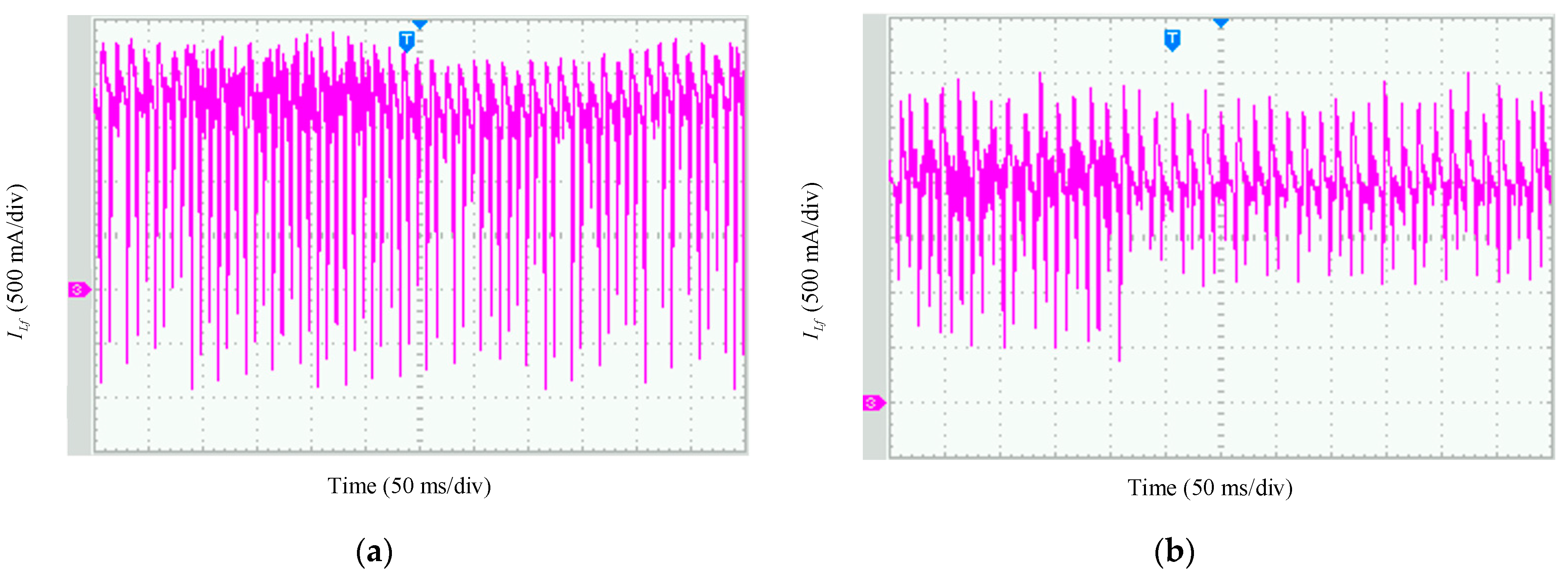
In the above simulation part, the anti-disturbance performance of the two controllers is carried out, and the disturbance experiment is also carried out in the same case. As can be seen from Figure 20, when the input voltage is reduced as a disturbance signal, the charging current under PI control has an influence after the disturbance and recovery process. The proposed method is almost unaffected by this disturbance. It can be seen that the active disturbance rejection controller has a stronger anti-disturbance ability than the PI control.
ADRC is a kind of control method that extracts the disturbance information from the input/output signal of the controlled object before the disturbance significantly affects the final output of the system and then uses the control signal to eliminate it as soon as possible, thus greatly reducing its influence on the controlled quantity.
6. Conclusions
In this paper, the application and working principle of a full-bridge DC–DC converter of pulse power supply are studied and analyzed. Considering the complex time-varying switching behavior of a full-bridge DC–DC converter, in order to control the trigger pulse cycle more accurately, and improve the anti-interference ability and dynamic performance of the system, a pulse power supply with a controllable charging time based on the theory of active disturbance rejection controllers is proposed. A LADRC controller is constructed to control the charging of the converter current, and then an inner loop current regulator is assembled to facilitate the control of dynamic performance. The resulting double closed-loop control structure improves the steady-state and transient current-tracking performance. Finally, the effectiveness of the proposed method is verified by the comparison simulation and experiment of the prototype.
The above-designed full-bridge DC–DC converter system of pulse power supply with a controllable charging time based on ADRC has the following limitations:
- If the system is applied to long-line applications, the stray parameters existing in the line will cause changes in the system parameters, which will bring difficulties to the design of the controller.
- Since the pulse discharge is used by the gas spark switch, continuous discharge will cause the ablation of the switching electrode, resulting in fluctuations in the discharge voltage.
For long-line applications, the parameter identification of the line system can be conducted in advance, and the line parameters can be accurately identified, which can lay a good foundation for the later controller design.
For the electrode ablation phenomenon of the gas spark switch, to avoid the fluctuation of discharge voltage, the electronic switch can be used to replace the gas spark switch.
This article is expected to provide more ideas for engineers to apply the ADRC in power electronic converter control.
Author Contributions
Z.K. proposed a current control method for pulsed power supply based on an LADRC; Y.L. performed the modeling and verified it by simulation and experiments and wrote the manuscript. All authors have read and agreed to the published version of the manuscript.
Funding
This research was funded by the National Natural Science Foundation of China, grant number 52241702, and Major National Science and Technology Projects of China, grant number 2016ZX05034004.
Institutional Review Board Statement
Not applicable.
Informed Consent Statement
Not applicable.
Data Availability Statement
Data are contained within the article.
Conflicts of Interest
The authors declare no conflict of interest.
References
- Davari, P.; Zare, F.; Ghosh, A.; Akiyama, H. High-Voltage Modular Power Supply Using Parallel and Series Configurations of Flyback Converter for Pulsed Power Applications. IEEE Trans. Plasma Sci. 2012, 40, 2578–2587. [Google Scholar] [CrossRef]
- Akiyama, H.; Sakugawa, T.; Namihira, T.; Takaki, K.; Minamitani, Y.; Shimomura, N. Industrial Applications of Pulsed Power Technology. IEEE Trans. Dielectr. Electr. Insul. 2007, 14, 1051–1064. [Google Scholar] [CrossRef]
- Elserougi, A.; Ahmed, S.; Massoud, A. High voltage pulse generator based on DC-to-DC boost converter with capacitor-diode voltage multipliers for bacterial decontamination. In Proceedings of the IECON 2015—41st Annual Conference of the IEEE Industrial Electronics Society, Yokohama, Japan, 9–12 November 2015. [Google Scholar]
- Nuccitelli, R. Nanosecond pulsed electric fields cause melanomas to self-destruct. In Proceedings of the Conference Record of the 2006 Twenty-Seventh International Power Modulator Symposium, Arlington, VA, USA, 14–18 May 2006. [Google Scholar]
- Sethian, J.D. Pulsed power for a rep-rate, electron beam pumped KrF laser. IEEE Trans. Plasma Sci. 2000, 28, 1333–1337. [Google Scholar] [CrossRef]
- Tsoi, T.; Whitworth, C.; Kim, M.; Bayne, S.; O’Brien, H.; Ogunniyi, A. SiC GTOs Thyristor for Long Term Reliability on Pulsed Power Application Test. In Proceedings of the 2021 IEEE Pulsed Power Conference (PPC), Denver, CO, USA, 12–16 December 2021. [Google Scholar]
- Collier, L.; Kajiwara, T.; Dickens, J.; Mankowski, J.; Neuber, A. Fast SiC Switching Limits for Pulsed Power Applications. IEEE Trans. Plasma Sci. 2019, 47, 5306–5313. [Google Scholar] [CrossRef]
- Nakayama, K.; Tanaka, Y.; Kato, T.; Kojima, K.; Sometani, M.; Yonezawa, Y. 10 kV SiC thyristor for High Voltage Pulsed Power Generators. In Proceedings of the 2023 IEEE Applied Power Electronics Conference and Exposition (APEC), Orlando, FL, USA, 19–23 March 2023. [Google Scholar]
- Liang, S.; Guo, J.; Liu, H.; Wang, J. Evaluation of High-Voltage 4H-SiC Gate Turn-off Thyristor for Pulsed Power Application. In Proceedings of the 2021 IEEE 1st International Power Electronics and Application Symposium (PEAS), Shanghai, China, 13–15 November 2021. [Google Scholar]
- Ren, X.; Xu, Z.-W.; Xu, K.; Zhang, Z.; Chen, Q. SiC Stacked-Capacitor Converters for Pulse Applications. IEEE Trans. Power Electron. 2019, 34, 4450–4464. [Google Scholar] [CrossRef]
- Redondo, L.M. A DC Voltage-Multiplier Circuit Working as a High-Voltage Pulse Generator. IEEE Trans. Plasma Sci. 2010, 38, 2725–2729. [Google Scholar] [CrossRef]
- Ahn, S.-H.; Ryoo, H.-J.; Gong, J.-W.; Jang, S.-R. Low-Ripple and High-Precision High-Voltage DC Power Supply for Pulsed Power Applications. IEEE Trans. Plasma Sci. 2014, 42, 3023–3033. [Google Scholar] [CrossRef]
- Zabihi, S.; Zare, F.; Ledwich, G.; Ghosh, A.; Akiyama, H. A new pulsed power supply topology based on positive buck-boost converters concept. IEEE Trans. Dielectr. Electr. Insul. 2010, 17, 1901–1911. [Google Scholar] [CrossRef]
- Zabihi, S.; Zare, F.; Ledwich, G.; Ghosh, A.; Akiyama, H. A Novel High-Voltage Pulsed-Power Supply Based on Low-Voltage Switch–Capacitor Units. IEEE Trans. Plasma Sci. 2010, 38, 2877–2887. [Google Scholar] [CrossRef]
- Yao, Y.; Krishnamoorthy, H.S.; Yerra, S. Linear Assisted DC/DC Converter for Pulsed Mode Power Applications. In Proceedings of the 2020 IEEE International Conference on Power Electronics, Smart Grid and Renewable Energy (PESGRE2020), Cochin, India, 2–4 January 2020. [Google Scholar]
- Safaee, A.; Jain, P.K.; Bakhshai, A. An Adaptive ZVS Full-Bridge DC–DC Converter With Reduced Conduction Losses and Frequency Variation Range. IEEE Trans. Power Electron. 2015, 30, 4107–4118. [Google Scholar] [CrossRef]
- Xie, Y.; Ghaemi, R.; Sun, J.; Freudenberg, J.S. Implicit Model Predictive Control of a Full Bridge DC–DC Converter. IEEE Trans. Power Electron. 2009, 24, 2704–2713. [Google Scholar] [CrossRef]
- He, H.; Si, T.; Sun, L.; Liu, B.; Li, Z. Linear Active Disturbance Rejection Control for Three-Phase Voltage-Source PWM Rectifier. IEEE Access 2020, 8, 45050–45060. [Google Scholar] [CrossRef]
- Su, Y.; Ge, X.; Xie, D.; Wang, K. An Active Disturbance Rejection Control-Based Voltage Control Strategy of Single-Phase Cascaded H-Bridge Rectifiers. IEEE Trans. Ind. Appl. 2020, 56, 5182–5193. [Google Scholar] [CrossRef]
- Tiwari, N.; Agarwal, P.; Srivastava, S.P. Performance investigation of modified hysteresis current controller with the permanent magnet synchronous motor drive. IET Electr. Power Appl. 2020, 4, 101–108. [Google Scholar] [CrossRef]
- Kang, B.J.; Liaw, C.M. A robust hysteresis current-controlled PWM inverter for linear PMSM driven magnetic suspended positioning system. IEEE Trans. Ind. Electron. 2021, 48, 956–967. [Google Scholar] [CrossRef]
- Zhang, X.; Hou, B.; Mei, Y. Deadbeat Predictive Current Control of Permanent-Magnet Synchronous Motors with Stator Current and Disturbance Observer. IEEE Trans. Power Electron. 2017, 32, 3818–3834. [Google Scholar] [CrossRef]
- Türker, T.; Buyukkeles, Y.; Bakan, A.F. A Robust Predictive Current Controller for PMSM Drives. IEEE Trans. Ind. Electron. 2016, 63, 3906–3914. [Google Scholar] [CrossRef]
- Liu, X.; Yu, H.; Yu, J.; Zhao, L. Combined Speed and Current Terminal Sliding Mode Control With Nonlinear Disturbance Observer for PMSM Drive. IEEE Access 2018, 6, 29594–29601. [Google Scholar] [CrossRef]
- Wang, L.; Chai, T.; Zhai, L. Neural-Network-Based Terminal Sliding-Mode Control of Robotic Manipulators Including Actuator Dynamics. IEEE Trans. Ind. Electron. 2009, 56, 3296–3304. [Google Scholar] [CrossRef]
- Qu, L.; Qiao, W. Active-Disturbance-Rejection-Based Sliding-Mode Current Control for Permanent-Magnet Synchronous Motors. IEEE Trans. Power Electron. 2021, 36, 751–760. [Google Scholar] [CrossRef]
- Chen, W. Indirect Input-Series Output-Parallel DC–DC Full Bridge Converter System Based on Asymmetric Pulse width Modulation Control Strategy. IEEE Trans. Power Electron. 2019, 34, 3164–3177. [Google Scholar] [CrossRef]
- Li, C.; Zhang, Y.; Cao, Z.; XU, D. Single-Phase Single-Stage Isolated ZCS Current-Fed Full-Bridge Converter for High-Power AC/DC Applications. IEEE Trans. Power Electron. 2017, 32, 6800–6812. [Google Scholar] [CrossRef]
- Kulasekaran, S.; Ayyanar, R. Analysis, Design, and Experimental Results of the Semidual-Active-Bridge Converter. IEEE Trans. Power Electron. 2014, 29, 5136–5147. [Google Scholar] [CrossRef]
- Jin, H.; Chen, Y.; Lan, W. Replacing PI Control With First-Order Linear ADRC. In Proceedings of the 2019 IEEE 8th Data Driven Control and Learning Systems Conference (DDCLS), Dali, China, 24–27 May 2019. [Google Scholar]
- Tian, G.; Gao, Z. Frequency Response Analysis of Active Disturbance Rejection Based Control System. In Proceedings of the 2007 IEEE International Conference on Control Applications, Singapore, 1–3 October 2007. [Google Scholar]
Figure 1.
Pulse power supply with controllable charging time.
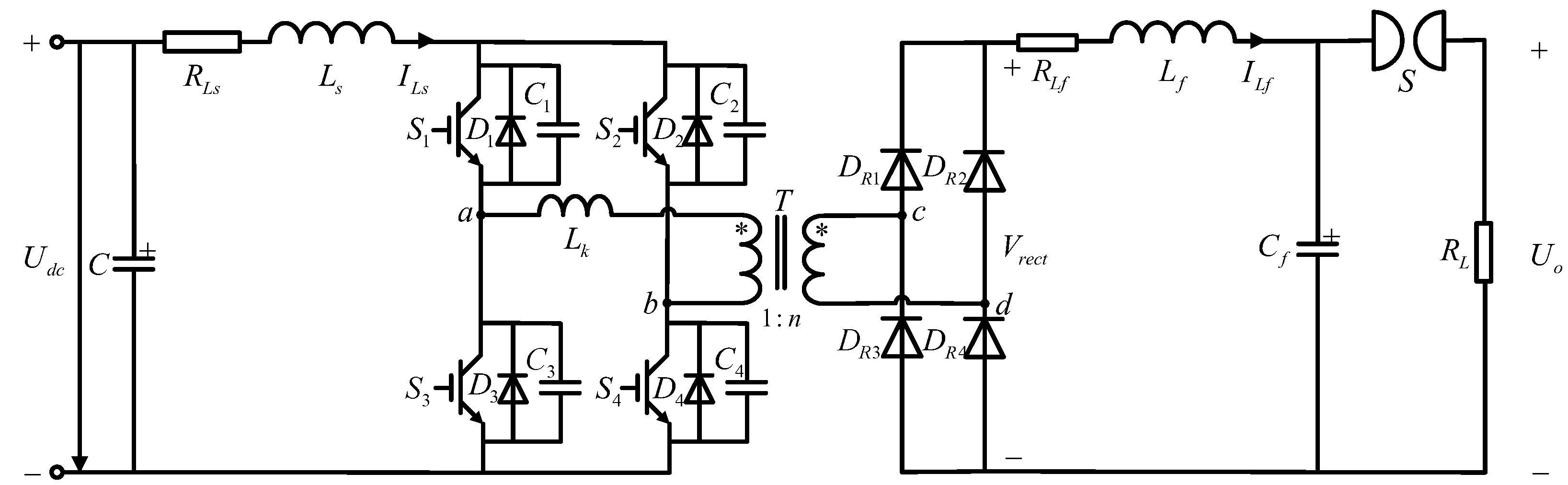
Figure 2.
Unipolar sinusoidal pulse width modulation scheme.

Figure 3.
Operation stages with USPWM. (a) The operating circuit of Interval 1; (b) the operating circuit of Interval 2.
Figure 3.
Operation stages with USPWM. (a) The operating circuit of Interval 1; (b) the operating circuit of Interval 2.
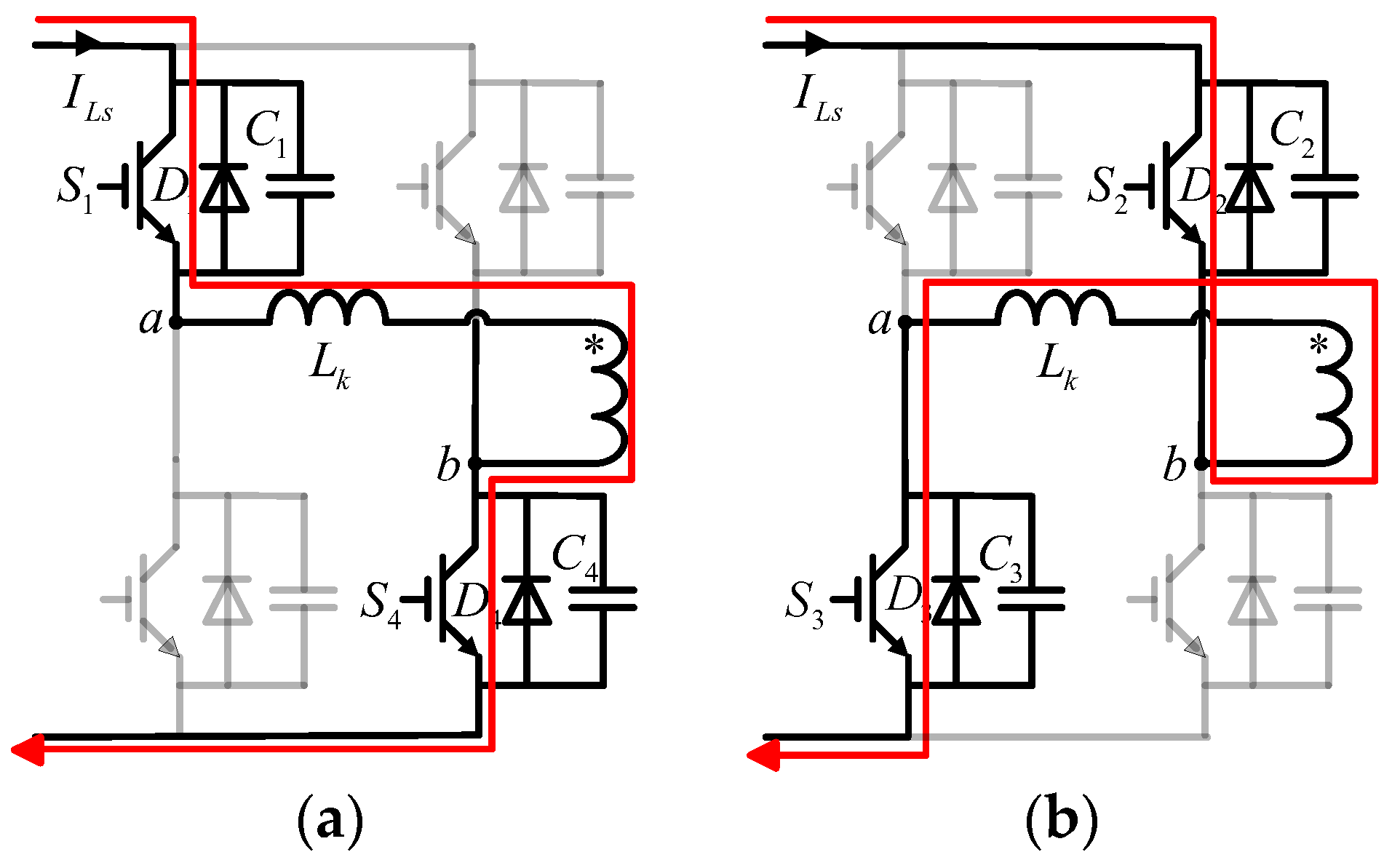
Figure 4.
Operating waveforms to illustrate the operation of the full-bridge DC–DC converter.

Figure 5.
Operation circuit. (a) Supplying circuit; (b) discharging circuit.

Figure 6.
The control structure of pulse power supply with controllable charging time.
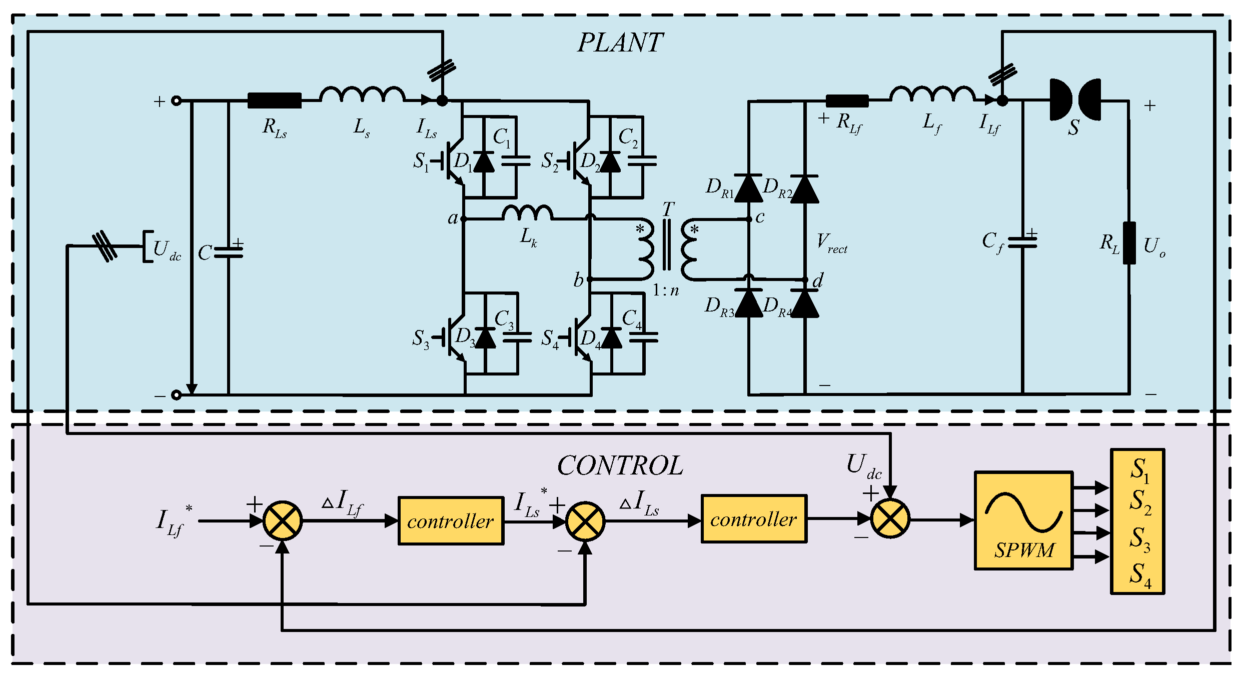
Figure 7.
Block diagram of the LADRC control.

Figure 8.
LADRC transfer function block diagram.

Figure 9.
The Bode diagram of the system: (a) Bode plot of by changing the controller bandwidth; (b) Bode plot of by changing the observer bandwidth.
Figure 9.
The Bode diagram of the system: (a) Bode plot of by changing the controller bandwidth; (b) Bode plot of by changing the observer bandwidth.

Figure 10.
Steady-state performance: (a) charge current responses under steady-state operation; (b) voltage waveform on capacitor .
Figure 10.
Steady-state performance: (a) charge current responses under steady-state operation; (b) voltage waveform on capacitor .

Figure 11.
PI-based robustness under parameter variations: (a) charge current response under leakage inductance variation; (b) voltage waveform on capacitor .
Figure 11.
PI-based robustness under parameter variations: (a) charge current response under leakage inductance variation; (b) voltage waveform on capacitor .
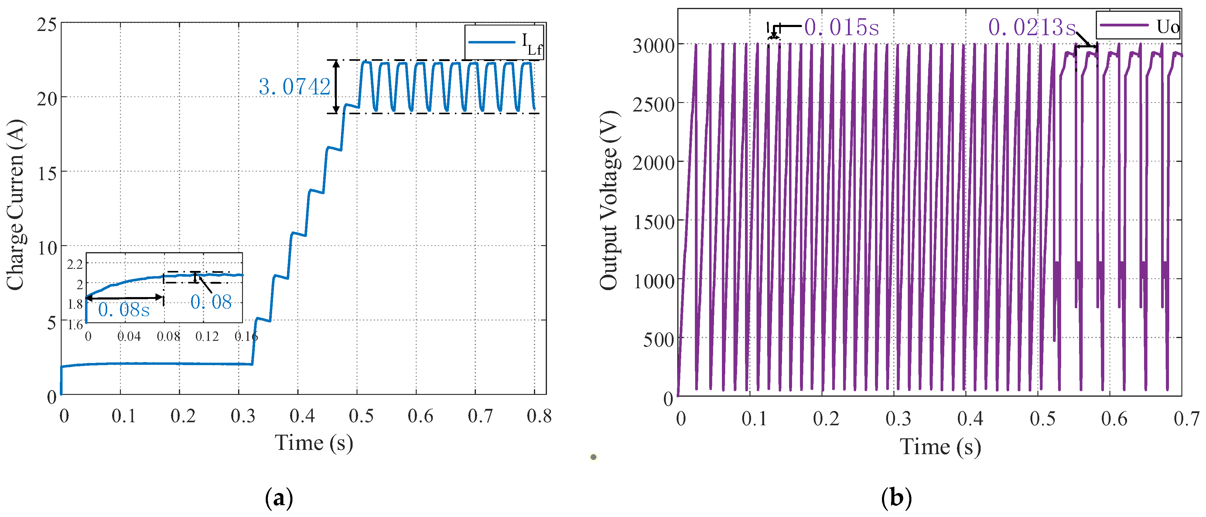
Figure 12.
ADRCI-based robustness under parameter variations: (a) charge current response under leakage inductance variation; (b) voltage waveform on capacitor .
Figure 12.
ADRCI-based robustness under parameter variations: (a) charge current response under leakage inductance variation; (b) voltage waveform on capacitor .
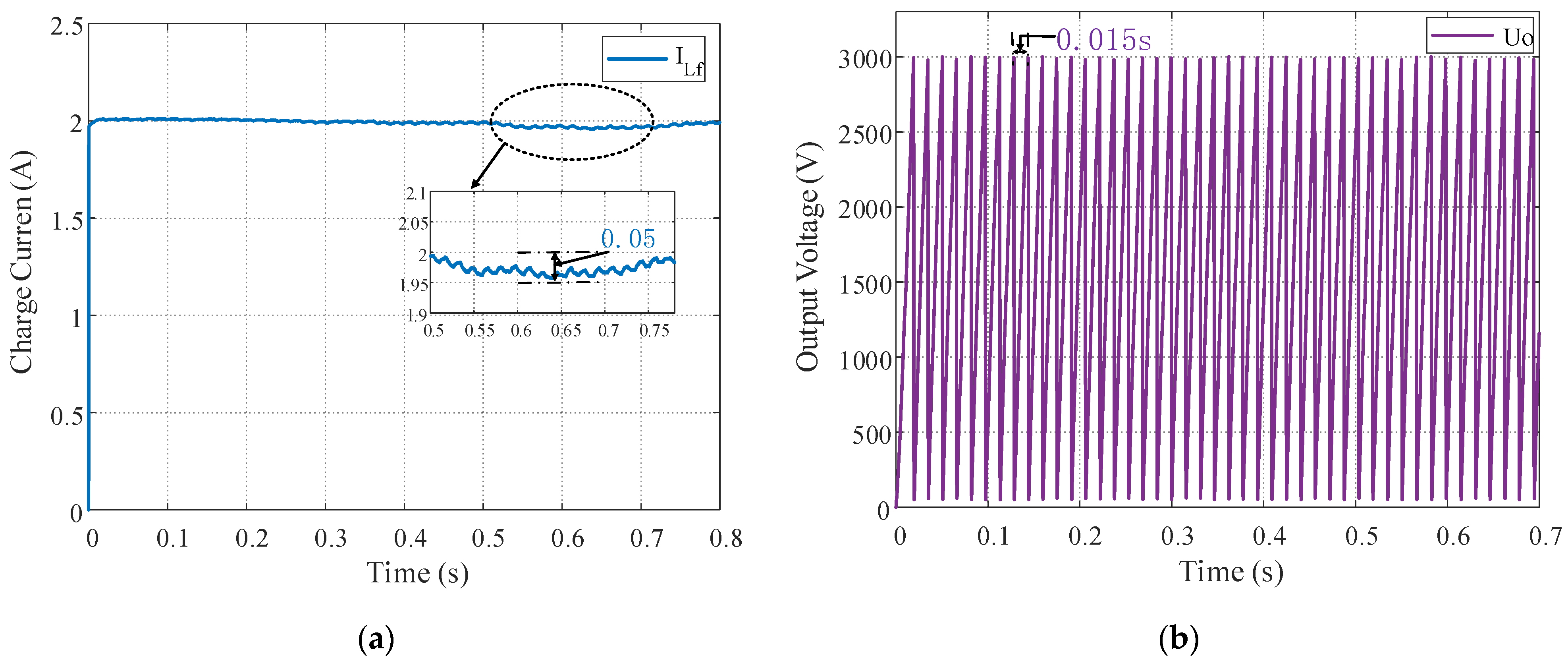
Figure 13.
Transient performance based on PI and ADRC: (a) PI-based control; (b) ADRC-based control.
Figure 13.
Transient performance based on PI and ADRC: (a) PI-based control; (b) ADRC-based control.

Figure 14.
Performance under disturbance based on PI control and ADRC control.
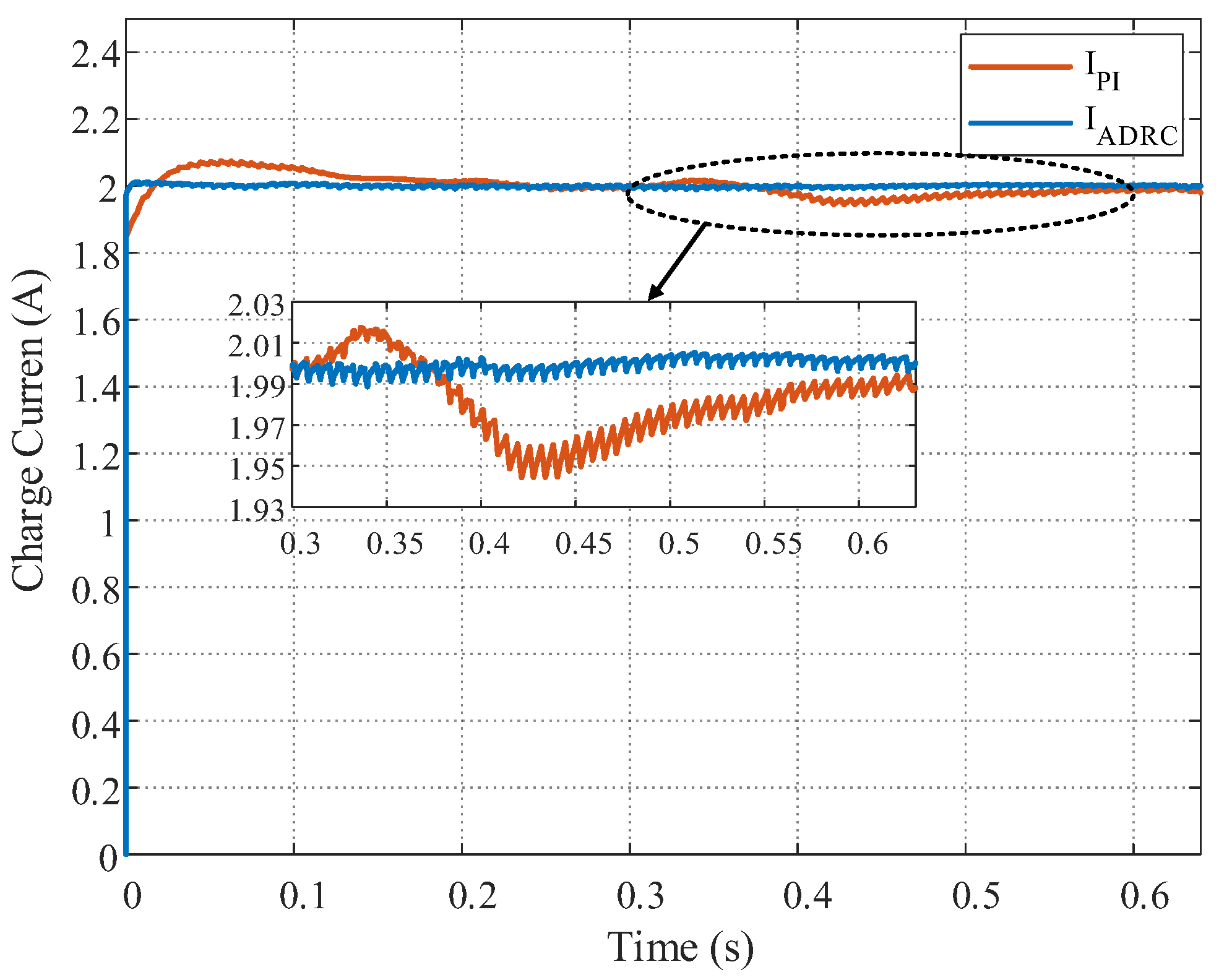
Figure 15.
Photograph of the experimental setup.
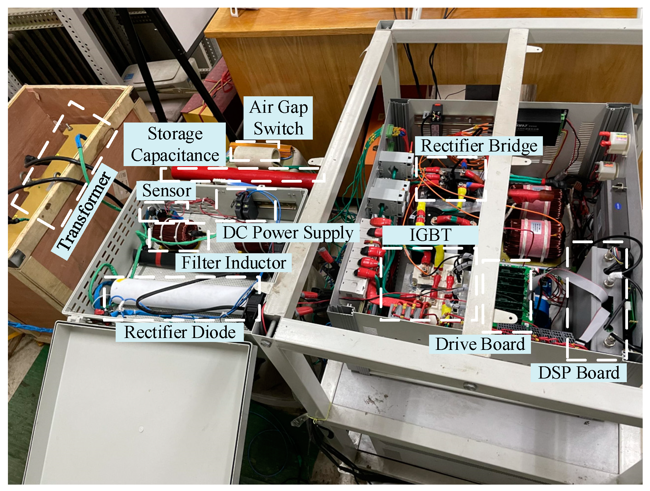
Figure 16.
Schematic of the experimental setup.
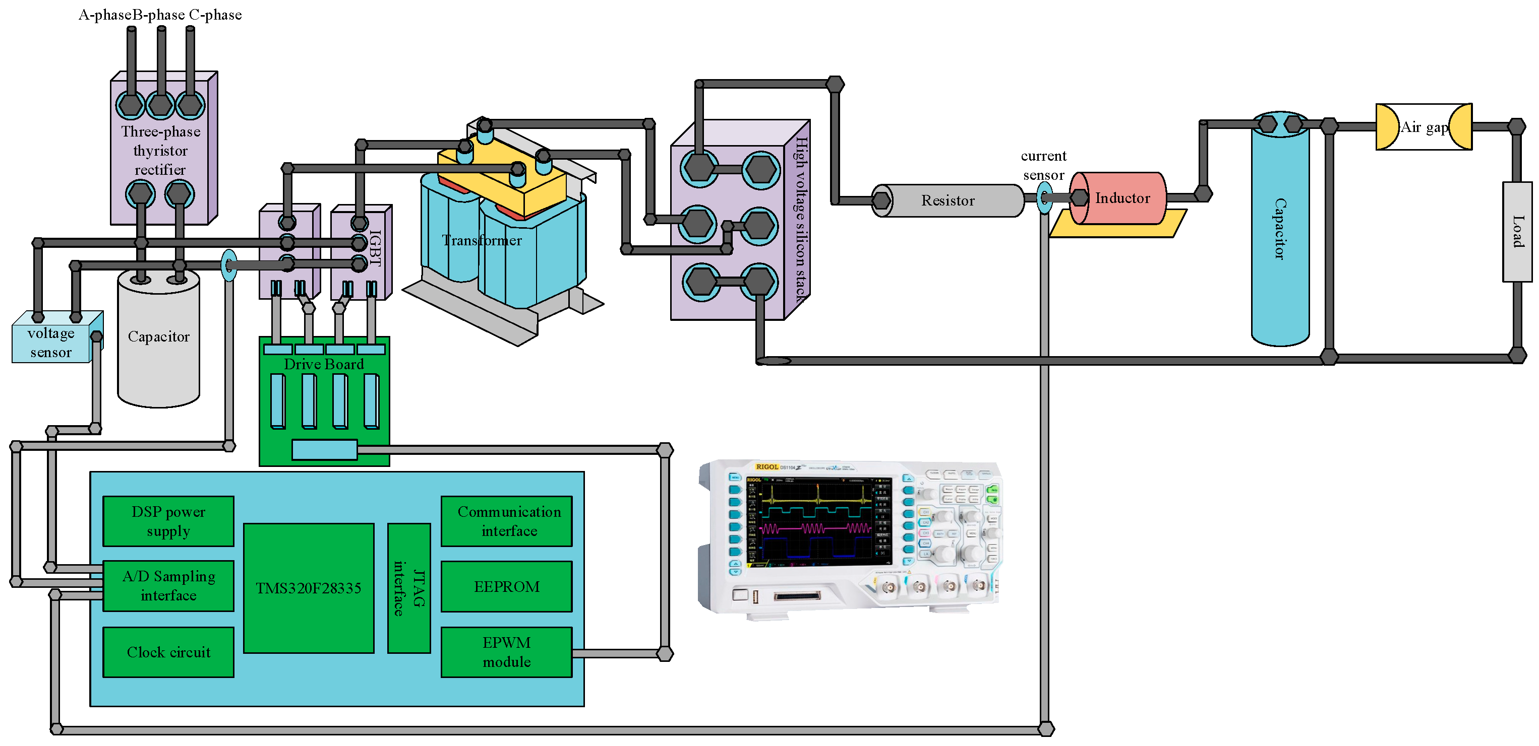
Figure 17.
Charge current responses waveform: (a) PI-based control; (b) LADRC-based control.

Figure 18.
Voltage waveform on capacitor : (a) PI-based control; (b) LADRC-based control.

Figure 19.
Comparison of voltage waveforms on the capacitor .
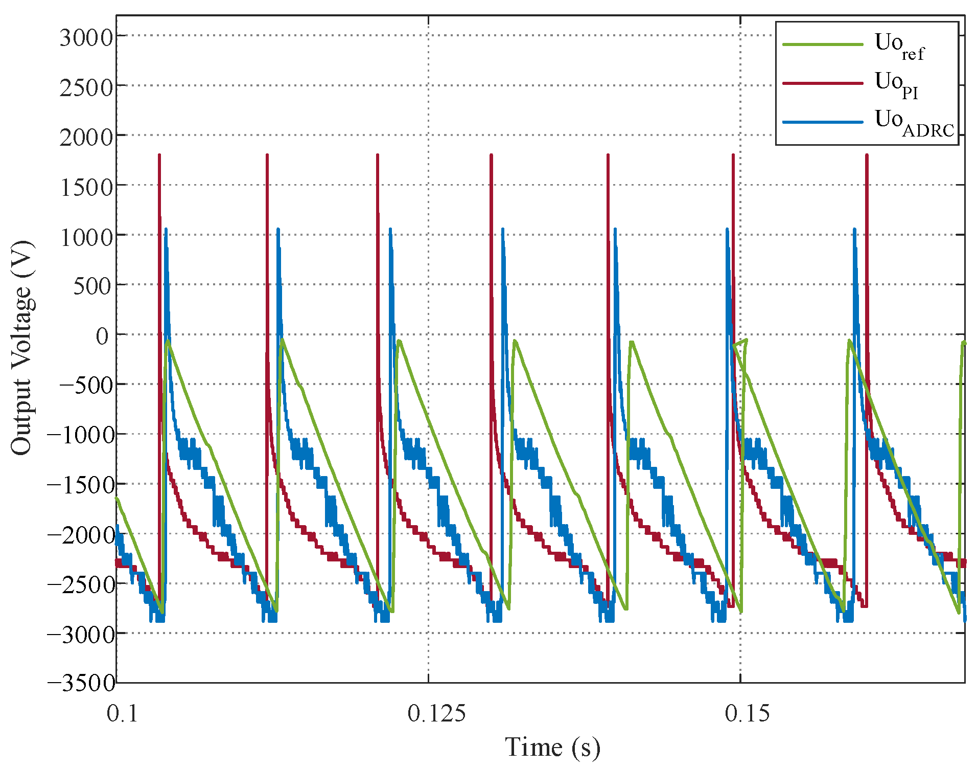
Figure 20.
Current performance under disturbance based on PI control and ADRC control: (a) PI-based control; (b) LADRC-based control.
Figure 20.
Current performance under disturbance based on PI control and ADRC control: (a) PI-based control; (b) LADRC-based control.

Table 1.
Pulse power supply system and control parameters.
| System Parameters | Symbols | Value |
| Input side DC voltage | 300 V | |
| Input side capacitor | 2350 | |
| Leakage induction of transformer | 10 | |
| Transformer ratio reciprocal | 36 | |
| Output side line impedance | 50 | |
| Output side inductor | 1.0 | |
| Output side capacitor | 10 | |
| Control Parameters | Symbols | Value |
| Proportional gain | 20 | |
| Integral gain | 100 | |
| Controller bandwidth | 500 | |
| Observer bandwidth | 1000 | |
| Compensation factor | 10 |
Disclaimer/Publisher’s Note: The statements, opinions and data contained in all publications are solely those of the individual author(s) and contributor(s) and not of MDPI and/or the editor(s). MDPI and/or the editor(s) disclaim responsibility for any injury to people or property resulting from any ideas, methods, instructions or products referred to in the content. |
© 2023 by the authors. Licensee MDPI, Basel, Switzerland. This article is an open access article distributed under the terms and conditions of the Creative Commons Attribution (CC BY) license (https://creativecommons.org/licenses/by/4.0/).
Share and Cite
MDPI and ACS Style
Kang, Z.; Li, Y. Active Disturbance Rejection Control of Full-Bridge DC–DC Converter for a Pulse Power Supply with Controllable Charging Time. Electronics 2023, 12, 5018. https://doi.org/10.3390/electronics12245018
AMA Style
Kang Z, Li Y. Active Disturbance Rejection Control of Full-Bridge DC–DC Converter for a Pulse Power Supply with Controllable Charging Time. Electronics. 2023; 12(24):5018. https://doi.org/10.3390/electronics12245018
Chicago/Turabian StyleKang, Zhongjian, and Yuntong Li. 2023. "Active Disturbance Rejection Control of Full-Bridge DC–DC Converter for a Pulse Power Supply with Controllable Charging Time" Electronics 12, no. 24: 5018. https://doi.org/10.3390/electronics12245018
Note that from the first issue of 2016, this journal uses article numbers instead of page numbers. See further details here.