
Design of a 0.4 V, 8.43 ENOB, 5.29 nW, 2 kS/s SAR ADC for Implantable Devices


1
Department of Electronics and Communication Engineering, V.F.S.T.R University, Vadlamudi, Guntur 522213, Andhra Pradesh, India
2
Department of Electronics and Communication Engineering, Mohan Babu University [Erstwhile Sree Vidyanikethan Engineering College], Tirupati 517102, Andhra Pradesh, India
3
Faculty of Electronics Telecommunications and Information Technology, Universitatea Nationala de Stiinta si Tehnologie Politehnica Bucuresti, 060042 Bucharest, Romania
*
Author to whom correspondence should be addressed.
Electronics 2023, 12(22), 4691; https://doi.org/10.3390/electronics12224691
Submission received: 4 September 2023
/
Revised: 30 October 2023
/
Accepted: 8 November 2023
/
Published: 18 November 2023
(This article belongs to the Special Issue CMOS Integrated Circuits Design)
Abstract
:This paper presents a 9-bit differential, minimum-powered, successive approximation register (SAR) ADC intended for implantable devices or sensors. Such applications demand nanowatt-range power consumption, which is achieved by designing the SAR ADC with a proposed bootstrap switch, bespoke split-capacitive DAC, customized comparator and a modified dynamic bit-slice unit for SAR logic. The linearity of the ADC is improved by introducing a bootstrap switch with a low clock feedthrough and threshold voltage variations along with the disseminated attenuation capacitor in the split-capacitive DAC. The dynamic comparator is customized to be simple in terms of the number of transistors to gain the advantage of low power and is also designed to have a low dynamic offset voltage. The stacking concept is embedded in the bit-slice unit of SAR logic to achieve reduced leakage power. This paper is concerned with how to contribute to low power consumption in all the aspects possible related to the implementation of the SAR ADC. With a 0.4 V supply and at 2 kS/s, the proposed ADC achieves an SNDR of 52.52 dB and a power consumption of 5.29 nW, resulting in a figure of merit (FOM) of 7.66 fJ/conversion-step.
1. Introduction
These days, many applications similar to vivo sensors, biomedical implantable devices or wireless guided devices utilize the SAR ADC over other ADC architectures [1,2,3]. This is owing to its advantages of being scaled down with the technology, as it uses the least analog circuitry, and the benefit of energy efficiency allows it to operate at ultra-low-power supply voltages, which is in demand for medical electronics. Also, for the digitization of the sensed biopotential signal, a moderate resolution (8–12 bits) with sampling frequencies between 1 kS/s and 1000 kS/s ADC may be sufficient, which is aptly fulfilled by the SAR ADC [4,5,6,7]. Considering low power as the main constraint, it is achieved by trading off speed in this paper with a low sampling rate of 2 kS/s.
The capacitive DAC utilized in SAR ADC forms one of the power-thirsty blocks [8,9]. Its power consumption is mainly due to the DAC’s switching activity as well as the total capacitance of the DAC. This paper mainly focuses on reducing the total capacitance of the DAC and, thus, reducing its area and power consumption. The majority of SAR ADCs utilize charge-scaling DACs to gain the advantage of low power dissipation, as the capacitive array does not dissipate static power. Furthermore, the offset of the DAC can also be easily compensated for if a switch capacitor circuit is used. However, the value of capacitors used in the DAC rises exponentially with the number of bits [10]. For this reason, charge-scaling DACs employed in high-resolution SAR ADCs suffer from problems like mismatch of the capacitors, large area, high power consumption and inaccuracy of the DAC [10,11,12].
These problems can be overcome by utilizing a split-capacitive DAC that incorporates an attenuation capacitor to split the charge-scaling DAC into two groups [10]. This method reduces the weight of the MSB capacitor, thus reducing the area and dynamic power dissipation and also improving the linearity errors. The DAC area can be further minimized by reducing the value of MSB capacitance by further splitting the DAC, as shown in [13]. This method reduces the area of the DAC by 47% in the case of 8-bit architecture and improves accuracy with small capacitor mismatches. Furthermore, the thermometer code is utilized for replacing C and 2C capacitors with three capacitors of value C. So, the maximum capacitance value used will only be the attenuation capacitance of 4C/3, and the mismatch will be between C and 4C/3. The modified split-capacitive DAC eliminates the use of thermometer code and extra logic gates to achieve the simplicity of using only one valued capacitor. The design is carefully considered in the proposed DAC to realize the entire DAC with only a single-valued capacitor C design, thus minimizing capacitor mismatches.
The comparator is a constituent block of the SAR ADC that consumes a considerable amount of power. To save power, the design of the comparator should be as simple as possible while simultaneously using a reduced number of CMOS transistors. Also, due to the presence of mismatches in the dynamic comparator, which have inherent positive feedback, there will be an input-referred offset voltage that has to be minimized as it creates linearity errors. Between the static offset voltage caused by transistor parameters and threshold variations, and the dynamic offset voltage caused by mismatches in the parasitic capacitances, this paper concentrates on reducing the dynamic offset voltage. From the analytically balanced model, an intuition about the main contributors of the offset is obtained and the design modifications are performed accordingly to minimize the offset. Top plate sampling has the advantage of eliminating the use of MSB-valued capacitance as the direct comparison after sampling with equal DACp and DACn voltages, generating the MSB bit. This reduces DAC area and power consumption but affects linearity. Hence, a bootstrap sampling switch is an incumbent as it reduces the possible linearity errors. A bootstrap switch is proposed in this paper and implemented in the SAR ADC.
On the other hand, organic field effect transistors have also been recently used in sensors in order to convert a biosignal into an electronic signal [14]. Often, the transducers are commanded by a complementary metal-oxide semiconductor (CMOS) circuitry. The advantages of the combination of implantable sensors, CMOS electronics and integration technologies have been revealed by many authors [15,16,17,18,19,20,21,22]. In 2019, Angotzi et al. presented an implantable CMOS biosensor for simultaneous large-scale neural recording. The increase in the number of simultaneous neural recordings was possible due to the 180 nm CMOS technology, which offered a power consumption of less than 6 μW per pixel and referred to noise around 7.5 μV, incorporated in an in vivo neuro-biosensor applied on rats [18]. In 2020, Harpaz et al. reported a CMOS-based sensor that integrated specific DNA strands and could be able to detect enoyl-CoA-hydratase-isomerase as an indicator of the presence of the Colletotrichum gloeosporioides fungi [19]. In 2023, Tran et al. described the first bioluminescent-paper-based biosensor for ATP, combining zeolitic imidazolate framework-8 as the metal–organic framework (MOF), luciferase as the key enzyme, a portable detector and a smart-phone-integrated CMOS [20]. In all these cases, a constant triadic demand needs to be solved: low power, low voltage and low noise must be harmonized within the electronic recording circuitry. Therefore, this paper contributes to the design of a low-power SAR ADC using a 45 nm CMOS process in all possible aspects related to the implementation of implantable sensors, as every sensor needs an ADC for its data to be digitized.
The paper is structured as follows. Section 2 portrays the SAR ADC inclusive architecture. Section 3 describes the ADC design and its implementation, which comprises the proposed bootstrap switch operation; a discussion about its linearity, customized comparator operation and calculation of its static and dynamic offset; and elucidates the modified split-capacitive DAC and dynamic bit-slice unit of the SAR logic block of the ADC in detail. Section 4 presents the simulation results of the proposed SAR ADC, and conclusions are drawn in Section 5.
2. SAR ADC Architecture
Figure 1 represents the proposed fully differential SAR ADC, designed using a novel bootstrap switch, modified split-capacitive DAC, SAR logic and the proposed dynamic comparator. The bootstrap switch is a necessary component in all SAR ADCs operated at low supply voltages to maintain a low resistance and to reduce the sampling distortion [21]. A differential architecture is used to avail the advantage of high common mode noise rejection and good linearity [23]. The designed dynamic comparator achieves low offset and consists of a lower number of transistors that aids in attaining low power consumption. The differential DAC voltages are compared by the comparator to generate a digital signal that produces a digital code through SAR logic, which is further fed back to the differential DAC to convert the same into an analog signal.
3. Implementation of Key CMOS Blocks
The basic building blocks of SAR ADC are two bootstrap switches, two capacitive DACs, a dynamic comparator and SAR control logic. The detailed description of each block is presented in the following subsections.
3.1. Proposed Bootstrap Switch
Figure 2a represents the proposed bootstrap switch circuit along with its layout shown in Figure 2b. When the clk signal is high, the sampling switch is turned off and the C1 capacitor pre-charges to supply voltage Vdd. In this design, is generated internally to reduce the transistor count and achieve low power. Later, when clk becomes low, the floating battery C1 charges the sampling transmission gate to Vdd + Vin. The source terminal of the transmission gate receives Vin, thus maintaining a constant Vgs that makes the sampling switch work in a deep linear region to provide low resistance in the direction of improving linearity.
As the transmission gate switch reduces the error and non-linearity caused by the charge injection, clock feedthrough and non-uniform on-resistance, a new bootstrapped S/H circuit is proposed, utilizing the transmission gate switch. The on-resistance and the change in voltage of the proposed S/H design can be written in (1) and (2), respectively. Moreover, the change in voltage expression excludes the overlap capacitance consideration as it is a very minimally impacting term.
where the subscripts n and p represent the nMOS and pMOS transistors of the transmission gate switch, respectively. Equation (1) shows that the resistance is independent of the input voltage but dependent on the threshold voltage. However, as Vth is proportional to the substrate to bulk voltage, connecting bulk to substrate overcomes this problem, and the Ron of the design is maintained constant and will be independent of input. Also, the resistance is very low as the switch is biased in a deep linear region. Good linear S/H circuits desire constant and low on-resistance, which is achieved by the proposed design. Moreover, the change in voltage at the output node of the sampling switch Equation (2) is also independent of the input voltage, further enhancing the linearity of the design. Another reason for high linearity is the reduced harmonic distortion due to the low gate capacitance of the sampling switch compared with other state-of-the-art designs.
In low-power applications, the body effect due to threshold variations is also the cause of non-linearity, and an attempt is made to improve this through the design. The bodies of Mp1 and Mp4 are connected to the high-voltage end of C1 to reduce the threshold voltage variations, thus reducing the linearity errors. Body effect is also minimized by using the transmission gate as a sampling switch that introduces differential clock feedthrough error, which is equal in amplitude and opposite in phase at the drain terminals of the transmission gate, thus reducing clock feedthrough error.
Most of the existing bootstrap switches have no direct discharge path; rather, they consist of transistors not driven by the clk signal. This introduces a delay in the switch, which is reduced in the proposed design by connecting the gates of the transmission switch to transistors that are directly driven by a clock. Moreover, care is taken in the design to have only one transistor in the discharge path in order to improve the speed of the circuit.
Direct connection of the input signal to the sources of the transmission gate ensures that the Vgs of the gate does not exceed Vdd. In this design, the typical value of C1 = 50 fF is approximately five times the parasitic capacitance of the transistor with a channel length of 45 nm. Reliability constraints and a load capacitance value of 1 pF are considered while choosing the transistor sizes in order to not violate the specifications.
To evaluate the performance of the proposed bootstrap switch, it is used as a sample and hold circuit and is simulated using cadence virtuoso 45 nm CMOS technology files with a supply voltage of 0.45 V by applying a sinusoidal input of 0.45 Vp-p at 0.2 KHz frequency using a sampling clock of 2 KHz frequency, suitable for in vivo biosensing applications [14,15,16,17,18]. The post-layout is shown as the transient simulation result in Figure 3a. For fair comparison, bootstrapped switches from [24,25] are re-simulated with the same input parameters and then compared. The power consumed by the proposed switch is 111.9 pW, which is 23.5% less than [24] and 18.6% less than the bootstrap switch proposed in [25] because the proposed circuit benefits from the advantage of a lower transistor count and simplicity in its design. Moreover, the simulated leakage power is only 19.9 pW, about 17.7% of the total power, which is not considerable; hence, the design is not enhanced with the leakage reduction techniques.
Lowering of the supply voltage is one of the techniques for low-power design, but the disadvantage of this practice is that it increases delay. As it is known that delay is inversely proportional to supply voltage and directly proportional to the threshold voltage, the increase in delay due to the lowered supply voltage can be compensated by reducing the threshold voltage. Hence, in this design, low-Vt devices are preferred to speed up the turn-on time of the sampling switch by 8.3% compared with the standard Vt, as shown in Figure 3b.
Figure 4 shows the simulated FFT plot of the proposed bootstrap as a sample and hold circuit that achieves an ENOB of 12.77 bits, SFDR of 79.16 dBc and SNR of 78.65 dB, which are reasonably good results at lower sampling rates compared with those mentioned in [24,25] that achieve similar results at higher sampling rates. Hence, the proposed bootstrap switch is a better choice to be used in biomedical applications as a sample and hold circuit, which requires a good ENOB and SNR at low frequencies with low power consumption.
3.2. Dynamic Comparator
Figure 5a represents the proposed dynamic comparator, intended to be used in SAR ADCs applicable in implantable sensors. In this circuit, when Clk is high, Mn1, Mn2 and Mn3 are ON, discharging the nodes 1 and 2 to ground. Subsequently, when Clk is low, Mp1 is turned on, bringing Mp2 and Mp3 to an ON state by making the Vgs of these transistors negative. Hence, nodes 1 and 2 are charged to Vdd. These nodes are then discharged to the ground based on the differential inputs applied to Mn4 and Mn5. Figure 5b represents the layout of the proposed dynamic comparator design.
The proposed design avails the advantage of employing the circuit with a single clock that speeds up the comparison process compared with other different clocks, such as those in [26,27]. This circuit also generates an output that could be directly used to drive the SAR logic block of SAR ADC, unlike the conventional process where the differential outputs of a comparator are fed to a latch that further drives the SAR logic. The proposed design from the output point of view avoids the use of a latch, thus saving the chip area and power. As the input-driven transistors are directly connected to the output nodes, the design is supposed to endure a considerable amount of kickback noise. However, as the gate to drain parasitic capacitance and a parallel combination of drain to bulk and source to bulk parasitic capacitance are associated with inputs in opposite directions, the difference of charge in these capacitances will add on to the input, thus producing a negligible amount of kickback noise. This has been verified by simulating the proposed design and the existing designs using the kickback noise test bench from [28], and the results are tabulated. Apart from saving power, this design also provides low offset, which is a key factor to enhance the performance of the comparator that, in turn, augments the performance of the whole ADC. Process variations lead to device mismatches, which is a primary source of offset [28,29,30]. There are two types of offsets: static and dynamic, where static offset is due to current factor and threshold variations between the devices while dynamic offset is due to parasitic capacitance variations [22]. In the proposed design, as Mn1, Mn2 and Mn3 are off during the comparison phase, they do not affect the offset value. Even though Mp1 is on during the same phase, it is out of the differential operation, so it does not have an influence on the static offset. To find the static offset voltage, the transistors Mp2 and Mp3 are in the saturation region as they are directly connected to the output nodes Outp and Outn, respectively, and the input differential transistors Mn4 and Mn5 are in the triode region as they simply act as voltage-controlled resistors. Hence, the currents from these transistors can be mentioned as follows:
Idsp2 = (µp2Cox/2) (W/L)p2 (Outp − Outn − Vtp2)2
Idsp3 = (µp3Cox/2) (W/L)p3 (Outn − Outp − Vtp3)2
Idsn4 = (µn4Cox) (W/L)n4 (Vp − Vtn4 − Vdsn4/2)Vdsn4
Idsn5 = (µn5Cox) (W/L)n5(Vn − Vtn5 − Vdsn5/2)Vdsn5
Consequently, utilizing these current equations from (3)–(6), the offset from the balanced method [22] is
where Rp2 is the constant resistance at Mp2, which is like the resistance at Mp3 under a balanced condition, i.e.,
Vos (Mn4,Mn5) = (Idsn4 − Idsn5) Rp2
Rp2 = 1/(µn2Cox) (W/L)p2 (Vd2)
Substituting (5), (6) and (8) in (7) and elaborating yields
Under the balanced condition,
where ∆µn = mobility variations and ∆Vtn represents threshold variations due to the mismatch between Mn4 and Mn5 transistors. Substituting (10)–(14) into (9) and simplifying would lead to
Let µn4Cox = µn & µn5Cox = µn + ∆µn
Vtn4 = Vtn & Vtn5 = Vtn + ∆Vtn
Vp = Vn = Vin
Vdsn4 = Vdsn5 = Vdsn
(W/L)n4 = (W/L)n5
In (15), if the lengths of the transistors are the same, then the variations in the mobility and threshold voltages are inversely proportional to the width of the differential transistor pair and directly proportional to the width of switch, producing constant resistance. Hence, static offset due to a differential pair can be reduced by increasing the size of the differential transistors and reducing the size of the cross-coupled pMOS transistors. However, as Mp2 and Mp3 are used to generate constant currents, a reduction in their size would also affect the offset voltage. Hence, the overall static offset of the comparator will be
Ϭ2OS = (Ϭ2∆VMn4-Mn5 + Ϭ2∆VMp2-Mp3)1/2
The static offset of the cross-coupled pMOS transistors is also inversely proportional to their widths as they generate constant current; so, in contrast to the abovementioned, the widths of these transistors must be increased. Hence, design care is taken regarding the aspect ratios to have a trade-off between offset voltage and transistor size. Simulations of offset contributed by each mismatch transistor pair are shown in Figure 6. As mentioned, Mn1, Mn2 and Mn3 are off during the comparison phase, and Mp1 is on but is not affected by the differential operation; hence, it does not influence the static offset.
As discussed, regarding the dynamic offset, it is due to the parasitic capacitance variations that can be obtained by equating the differential output voltages as described in the balanced method [22], dOutp/dt = dOutn/dt, which means
and
equating the differential outputs
Applying the square law model to overwrite the drain source current in terms of voltage, the offset voltage due to mismatches in Cp and Cn is derived as
Hence, this proves that dynamic offset depends on relative capacitance mismatch rather than absolute capacitance mismatch. So, this dynamic offset is reduced by the following:
- Increasing the transistor sizes of the differential pair;
- Matched capacitors can be added at the output nodes to reduce the relative mismatch;
- Constant current can be generated into the output nodes.
By the end of the comparison phase, both the output nodes Outp and Outn are pulled down to ground by the differential pair of transistors due to which Mp2 and Mp3 will enter saturation. Subsequently, during the reset phase, Mp1 turns ON, forming ac as a code current source path along with Mp2 and Mp3 to both the output nodes Outp and Outn, respectively. This produces constant drain currents. In a while, at the beginning of the comparison phase, when one of the output nodes is low, the cross-coupled pMOS transistor driven by the same output node will be in saturation, generating a constant current that makes a stable current to flow in the other branch too, as they are cross-coupled. Hence, through this design, constant drain currents are generated to the output nodes to reduce the dynamic offset. The geometric dimensions followed in this design to obtain the optimized offset voltage are revealed in Table 1.
Table 2 presents the post-layout simulation results of the proposed comparator. It includes a comparative analysis of the proposed circuit with the referenced comparators, which are also simulated at 45 nm for equivalence. The design has a comparatively low offset due to its simple circuitry and careful sizing of the transistors in the circuit. Ref. [31] has lesser kickback noise due to its three-stage network, which isolates the input from the output strongly but at the cost of power consumption. Refs. [21,32] have low delay due to less cascaded transistors from supply rail to output. But the proposed one proves that the design is efficient and can be sufficiently used in low-power applications with less offset voltage. Moreover, the leakage power calculated for the design is only 51.4 pW, which is barely 4.8% of the total power. The kickback noise simulated is 2 mV, which is comparatively lower owing to the addition of the difference of the charge in the parasitic capacitance associated with the input nodes.
3.3. Modified Distributed Attenuation Capacitor Split-Capacitive DAC
Capacitive DAC is one of the main blocks of SAR ADC that consumes significant power. In a weighted capacitive DAC, the capacitance value increases with the number of bits; hence, a split-capacitive DAC was used that availed the advantages of low chip area and, thus, low power dissipation and high speed, but the fractional value of the attenuation capacitor produces mismatch errors [12]. For this reason, a distributed attenuation capacitor split-capacitive DAC was proposed in [13] that used capacitors of a single value to generate an 8 bit. In this paper, multiple attenuation capacitors are used instead of a single attenuation capacitor so that the MSB-driven capacitance value can be far reduced to 2C instead of 8C, as in a conventional split-capacitor DAC for an 8-bit ADC.
This saves about 47% of the chip area and reduces the capacitive mismatch errors as the capacitance values utilized are only C, 2C and 4C/3. [13] It further reduces the mismatch by replacing the 2C capacitance value with three capacitors of value C using a thermometer coding technique. This is represented in Table 3, and its circuit implementation is presented in Figure 7. However, this will still retain the mismatch between C and 4C/3 capacitance values and has an area overhead of using thermometer encoding. Also, realization of fractional-valued capacitance may introduce error. Hence, it is preferable to realize the entire ADC using a single-valued capacitance.
The modified distributed attenuation capacitor split-capacitive DAC proposed in this paper avoids the use of thermometer encoding, retaining the advantage of using the capacitance value of only C in the DAC part to which the bits are applied. The truth table in Table 3 can be modified in Table 4.
The proposed truth table, a modified form of the binary to thermometer decoding technique, is designed to represent the output codes (21–22) in terms of input bits to avoid the use of digital circuitry, as implemented in Figure 7.
Thus, the use of digital circuitry is avoided to save area and power consumption. So, now, the mismatch in the DAC would be with the C-valued capacitors through which bits from SAR logic are applied and an attenuation capacitor of value 4C/3. To represent the entire DAC in terms of unit capacitors, the attenuation capacitor is rearranged with the capacitors of value C to obtain the value 4C/3. Hence, minimizing the mismatch errors and limiting the maximum capacitance value used in the 9-bit DAC to value C to reduce the charging and discharging time of the capacitor improves the speed of the device. Here, the shortcoming is the parasitic capacitance associated with each capacitance that may deteriorate the capacitance equivalence. However, as the circuit is designed for low-frequency signals, this would not be of much use. The implementation of the modified DAC is shown in Figure 1, where MSB comparison is performed through top plate implementation and the remaining 8-bit DAC is split into three sub-DACs with a maximum capacitance of 2C, which is further split as per Table 4 into C and C, to which the MSB bit of the sub-DAC is applied. Attenuation capacitor representation is also shown in Figure 1. As the purpose of the paper is to showcase the use of split-capacitive DAC and overcome its problem of using a fractional attenuation capacitor, an energy switching scheme was not incorporated. But with the use of efficient energy switching schemes like in [34,35], better results could be incorporated.
3.4. SAR Logic
SAR control logic is implemented using dynamic logic as a substitute for complementary logic because its realization requires less transistors, thus offering better performance in terms of speed and power consumption [36]. But in this, at lower sampling rates, the leakage currents on the side of the output nodes of the bit-slice unit cause decision error at the P and N nodes of the logic. Hence, it is implemented using dynamic latch logic in [37] to eliminate the decision error caused by the leakage current. Accordingly, when the comparator output is ready, the positive feedback circuit latches the comparator outputs Outp and Outn to the P and N nodes, respectively, and are held constantly until there is a change in the comparator outputs, henceforth reducing the problem of leakage current. In the case of a proposed comparator design, the outputs are either differential in the comparison phase or grounded during the reset phase. As already mentioned, the bit-slice unit in [37] works well with the differential outputs, but when the comparator outputs are zero, leakage current might still exist.
This can be overcome by using a stacking of transistors technique to reduce leakage currents, reducing the leakage power thereafter. Figure 8 represents the modified SAR control logic designed by stacking the transistors driven by the comparator outputs in the bit-slice unit of [37]. Table 5 mentions the leakage power comparison of the bit-slice unit modified with that of the units from [36,37]. It proves that a stacked transistor bit-slice unit has low leakage power, thus contributing to the low power consumption of the entire SAR logic block.
4. Simulation Results of the Proposed ADC
The proposed 9-bit SAR ADC is simulated using a 45 nm CMOS process with a supply voltage of 0.4 V and a sampling rate of 2 kS/s. The simulated results are presented and discussed below.
4.1. Static Performance
Figure 9a,b show the simulated differential non-linearity (DNL) and integral nonlinearity (INL) of the proposed SAR ADC. The DNL is in the range of −0.10/+0.13 LSB while the INL is within −0.8/+0.5 LSB. These values agree with the linearity range demand [14,17,20]. These are due to small changes in the output codes related to the MSB capacitor as it switches from low to high. This may be owing to the effect of the parasitic capacitance on the output.
4.2. Dynamic Performance
Figure 10a shows the simulated FFT spectrum of the proposed SAR ADC with a 0.4 V, 8 Hz sinusoidal input signal with a 0.4 V supply and 2 kS/s sampling rate. The obtained signal-to-noise ratio (SNR) is 56.63 dB, equivalent to an effective number of bits (ENOB) of 8.43 bits and a spurious-free dynamic range (SFDR) of 57.14 dB. Figure 10b plots the simulated SNDR, SFDR and THD against the input frequencies that remain almost constant up to 7 KHz and drop later.
4.3. Power Performance
Leakage power is usually in terms of nW, which is the total power consumption of the entire ADC designed for low-frequency, medium-resolution, low-power applications. Hence, in this design, leakage power is reduced to reduce the overall power consumption of the ADC and care is taken in the design to propose each block with the minimum number of transistors and to avoid the static power consumption. Table 6 summarizes the simulation results of the proposed ADC. From the data obtained, the design consumes only 5.29 nW in total.
Figure 11 shows the power consumption of each block. As the total array capacitance of DAC is 620 fF, it consumes a large portion of the power.
To compare the power efficiency of the ADCs designed with different technologies and topologies, with various sampling rates and resolutions, the commonly cited figure of merit (FOM) is used for comparison:
The FOM of the proposed ADC is 7.66 fJ/conv. step at 2 kS/s, lower than the referred noise for implantable devices [18].
Table 7 represents the comparative analysis of the ADCs picked through the literature survey of low-power ADCs, having lower sampling frequencies, with the proposed 9-bit ADC. Because of their excellence in terms of achieving low power, some of the earlier works were also taken into consideration for comparison. The comparison proved that the proposed ADC has comparatively low power consumption, but [28] has the least. This is due to the fact that it is implemented using a power gating technique that reduces the leakage power; the same technique can be utilized in the proposed design to further enhance the power saving. Yet, the FOM of the proposed design portrays its efficiency. Ref. [31] is efficient in terms of achieving good SNDR due to the three amplification phases of the comparator used in the ADC that reduce the overall flicker noise and decouple the NTF zeros from the attenuation factor, allowing further reductions in noise. But the complex circuitry and generation of non-overlapping clocks made the designer to look for an alternative. Ref. [38] uses a body-driven technique in bootstrapped switches, SAR logic and a comparator to minimize leakage power consumption. In addition, a dynamic comparator with a floating inverter amplifier (FIA) architecture was designed to reduce the noise and offset by reducing the noise current. As a result, low power and good SNDR were achieved. However, as it uses a bulk-driven technique, it has low gain due to less transconductance compared with gate-driven and, thus, the efficiency of the circuit is low. The appreciating concern is that the proposed design achieves almost similar results using gate-driven transistors. Fabricated results may vary the simulated results by 10%, which would still prove the competence of the proposed design with the state-of-the-art low-power SAR ADCs included in [39,40,41,42,43,44,45,46].
5. Conclusions
This paper has presented an ultra-low-power SAR ADC intended for low-frequency, implantable bio-devices. The proposed ADC uses a modified split-capacitive DAC that uses a single-valued capacitor in order to reduce mismatch errors and a novel bootstrap switch to improve linearity and reduce power consumption. A dynamic comparator is also proposed that achieves a lower offset value and saves power through its design as it has a lower transistor count and a modified SAR control logic that implements stacked transistors to reduce leakage currents, thus contributing to power saving, as the SAR logic block is one of the power-hungry blocks of SAR ADC. The simulation results of the proposed ADC have verified the effectiveness of the design. The design achieves an ENOB of 8.43 bits at 2 kS/s with an overall power consumption of 5.29 nW and a FOM of 7.66 fJ/conversion-step, which are the minimal performances demanded in the biosensing area, to the best of our knowledge. Hence, the proposed ADC is also a serious candidate for the analog front-end circuitry that accompanies the usual implantable device applications.
Author Contributions
Conceptualization, P.V.L. and S.M.; methodology, P.V.L. and C.R.; software, P.V.L.; validation, S.M. and A.S.; resources, S.M. and A.S.; writing—original draft preparation, P.V.L.; writing—review and editing, S.M., A.S. and C.R.; visualization, S.M.; supervision, A.S.; project administration, A.S. and C.R.; funding acquisition, C.R. All authors have read and agreed to the published version of the manuscript.
Funding
In the case of acceptance, the APC of this research was funded by Universitatea Nationala de Stiinta si Tehnologie Politehnica Bucuresti, grant PubArt.
Informed Consent Statement
Not applicable.
Data Availability Statement
Data is contained within the article.
Conflicts of Interest
The authors declare no conflict of interest.
References
- Gregoire, B.R.; Musah, T.; Maghari, N.; Weaver, S.; Moon, U. A 30% beyond VDD signal swing 9-ENOB pipelined ADC using a 1.2V 30dB loop-gain opamp. In Proceedings of the IEEE Asian Solid-State Circuits Conference, Jeju, Republic of Korea, 14–16 November 2011; pp. 345–348. [Google Scholar] [CrossRef]
- Maghari, N.; Moon, U. A Third-Order DT ∆Ʃ Modulator Using Noise-Shaped Bi-Directional Single-Slope Quantizer. IEEE J. Solid-State Circuits 2011, 46, 2882–2891. [Google Scholar] [CrossRef]
- Chahardori, M.; Sharifkhani, M.; Sadughi, S. A 4-Bit, 1.6 GS/s Low Power Flash ADC, Based on Offset Calibration and Segmentation. IEEE Trans. Circuits Syst. I Regul. Pap. 2013, 60, 2285–2297. [Google Scholar] [CrossRef]
- Huang, G.; Chang, S.; Liu, C.; Lin, Y. A 1-µW 10-bit 200-kS/s SAR ADC With a Bypass Window for Biomedical Applications. IEEE J. Solid-State Circuits 2012, 47, 2783–2795. [Google Scholar] [CrossRef]
- Navidi, S.M.; Ehsanian, M. A 9-bit Low-Power Fully Differential SAR ADC Using Adaptive Supply and Reference Voltages. In Proceedings of the Iranian Conference on Electrical Engineering (ICEE), Mashhad, Iran, 8–10 May 2018; pp. 205–210. [Google Scholar] [CrossRef]
- Yaul, F.M.; Chandrakasan, A.P. 11.3 A 10b 0.6nW SAR ADC with data-dependent energy savings using LSB-first successive approximation. In Proceedings of the International Solid-State Circuits Conference Digest of Technical Papers (ISSCC), San Francisco, CA, USA, 9–13 February 2014; pp. 198–199. [Google Scholar] [CrossRef]
- Yadav, K.; Patra, P.; Dutta, A. A 43-nW 10-bit 1-kS/s SAR ADC in 180nm CMOS for biomedical applications. In Proceedings of the Asia Pacific Conference on Postgraduate Research in Microelectronics and Electronics (PrimeAsia), Hyderabad, India, 27–29 November 2015; pp. 21–25. [Google Scholar] [CrossRef]
- Liu, C.; Chang, S.; Huang, G.; Lin, Y. A 0.92mW 10-bit 50-MS/s SAR ADC in 0.13μm CMOS process. In Proceedings of the Symposium on VLSI Circuits, Kyoto, Japan, 16–18 June 2009; pp. 236–237. [Google Scholar]
- Chen, Y.; Zhu, X.; Tamura, H.; Kibune, M.; Tomita, Y.; Hamada, T.; Yoshioka, M.; Ishikawa, K.; Takayama, T.; Ogawa, J.; et al. Split capacitor DAC mismatch calibration in successive approximation ADC. In Proceedings of the IEEE Custom Integrated Circuits Conference, San Jose, CA, USA, 13–16 September 2009; pp. 279–282. [Google Scholar] [CrossRef]
- Baker, R.J. CMOS: Circuit Design, Layout and Simulation; John Wiley & Sons: Hoboken, NJ, USA, 2011; Volume 18. [Google Scholar]
- Maloberti, F. Data Converters 1; Springer: Berlin/Heidelberg, Germany, 2007; Available online: www.springer.com/gp/book/9780387324852 (accessed on 31 January 2023).
- Osipov, D.; Guscv, A.; Paul, S. By Design Correction of Capacitors Mismatch in SAR ADC with Split Capacitor DAC. In Proceedings of the 2021 IEEE 32nd International Conference on Microelectronics (MIEL), Nis, Serbia, 12–14 September 2021; pp. 209–212. [Google Scholar] [CrossRef]
- Nazari, M.; Aghajani, A.; Hashemipour, O. Design of a new split-capacitive-array DAC based on distribution of attenuation capacitor. In Proceedings of the 23rd Iranian Conference on Electrical Engineering, Tehran, Iran, 10–14 May 2015; pp. 1370–1373. [Google Scholar] [CrossRef]
- Segantini, M.; Parmeggiani, M.; Ballesio, A.; Palmara, G.; Frascella, F.; Marasso, S.L.; Cocuzza, M. Design of a Portable Microfluidic Platform for EGOT-Based in Liquid Biosensing. Sensors 2022, 22, 969. [Google Scholar] [CrossRef] [PubMed]
- Tran, D.P.; Pham, T.T.T.; Wolfrum, B.; Offenhäusser, A.; Thierry, B. CMOS-Compatible Silicon Nanowire Field-Effect Transistor Biosensor: Technology Development toward Commercialization. Materials 2018, 11, 785. [Google Scholar] [CrossRef]
- Hamza, M.N.; Abdulkarim, Y.I.; Saeed, S.R.; Altıntaş, O.; Mahmud, R.H.; Appasani, B.; Ravariu, C. Low-Cost Antenna-Array-Based Metamaterials for Non-Invasive Early-Stage Breast Tumor Detection in the Human Body. Biosensors 2022, 12, 828. [Google Scholar] [CrossRef] [PubMed]
- Zhang, M.; Adkins, M.; Wang, Z. Recent Progress on Semiconductor-Interface Facing Clinical Biosensing. Sensors 2021, 21, 3467. [Google Scholar] [CrossRef]
- Angotzi, G.N.; Boi, F.; Lecomte, A.; Miele, E.; Malerba, M.; Zucca, S.; Casile, A.; Berdondini, L. SiNAPS: An implantable active pixel sensor CMOS-probe for simultaneous large-scale neural recordings. Biosens. Bioelectron. 2019, 126, 355–364. [Google Scholar] [CrossRef]
- Harpaz, D.; Alkan, N.; Eltzov, E. The Incorporation of Amplified Metal-Enhanced Fluorescence in a CMOS-Based Biosensor Increased the Detection Sensitivity of a DNA Marker of the Pathogenic Fungus Colletotrichum gloeosporioides. Biosensors 2020, 10, 204. [Google Scholar] [CrossRef]
- Martínez-Pérez-Cejuela, H.; Calabretta, M.M.; Bocci, V.; D’Elia, M.; Michelini, E. Super-Stable Metal–Organic Framework (MOF)/Luciferase Paper-Sensing Platform for Rapid ATP Detection. Biosensors 2023, 13, 451. [Google Scholar] [CrossRef]
- Zhu, Z.; Liang, Y. A 0.6-V 38-nW 9.4-ENOB 20-kS/s SAR ADC in 0.18-µm CMOS for Medical Implant Devices. IEEE Trans. Circuits Syst. I Regul. Pap. 2015, 62, 2167–2176. [Google Scholar] [CrossRef]
- He, J.; Zhan, S.; Chen, D.; Geiger, R.L. Analyses of Static and Dynamic Random Offset Voltages in Dynamic Comparators. IEEE Trans. Circuits Syst. I Regul. Pap. 2009, 56, 911–919. [Google Scholar] [CrossRef]
- Yu, L.; Wang, X.; Wang, L. A low-power fully differential reconfigurable biomedical electronics interface to detect heart signals. In Proceedings of the Asia Pacific Conference on Postgraduate Research in Microelectronics and Electronics (PrimeAsia), Shanghai, China, 22–24 September 2010; pp. 400–403. [Google Scholar] [CrossRef]
- Chen, H.; He, L.; Deng, H.; Yin, Y.; Lin, F. A high-performance bootstrap switch for low voltage switched-capacitor circuits. In Proceedings of the IEEE International Symposium on Radio-Frequency Integration Technology, Hefei, China, 27–30 August 2014; pp. 1–3. [Google Scholar] [CrossRef]
- Liu, S.; Shen, Y.; Zhu, Z. A 12-Bit 10 MS/s SAR ADC With High Linearity and Energy-Efficient Switching. IEEE Trans. Circuits Syst. I Regul. Pap. 2016, 63, 1616–1627. [Google Scholar] [CrossRef]
- Babayan-Mashhadi, S.; Lotfi, R. Analysis and Design of a Low-Voltage Low-Power Double-Tail Comparator. IEEE Trans. Very Large Scale Integr. (VLSI) Syst. 2014, 22, 343–352. [Google Scholar] [CrossRef]
- Gao, J.; Li, G.; Li, Q. High-speed low-power common-mode insensitive dynamic comparator. Electron. Lett. 2015, 51, 134–136. [Google Scholar] [CrossRef]
- Diaz-Madrid, J.A.; Domenech-Asensi, G.; Hauer, J.; Mateu, L. A low kickback fully differential dynamic comparator for pipeline analog-to-digital converters. Eng. Rep. 2019, 1, e12055. [Google Scholar] [CrossRef]
- Rodrigues, S.; Bhat, M.S. Impact of Process Variation Induced Transistor Mismatch on Sense Amplifier Performance. In Proceedings of the International Conference on Advanced Computing and Communications, Surathkal, Mangalore, India, 20–23 December 2006; pp. 497–502. [Google Scholar] [CrossRef]
- Pinto, A.; Fernandes, J.D.S.R. A Study on the Offset Voltage of Dynamic Comparators. Des. Circuits Integr. Syst. 2012, 347–352. [Google Scholar]
- Hu, J.; Li, D.; Liu, M.; Zhu, Z. A 10-kS/s 625-Hz-Bandwidth 65-dB SNDR Second-Order Noise-Shaping SAR ADC for Biomedical Sensor Applications. IEEE Sens. J. 2020, 20, 13881–13891. [Google Scholar] [CrossRef]
- Yan, N.; Kang, C.; Mu, G.; Chen, S.; Wang, M.; Min, H. A 10-bit 16-MS/s Ultra Low Power SAR ADC for IoT Applications. In Proceedings of the 14th IEEE International Conference on Solid-State and Integrated Circuit Technology (ICSICT), Qingdao, China, 31 October–3 November 2018; pp. 1–3. [Google Scholar] [CrossRef]
- Liu, C.; Chang, S.; Huang, G.; Lin, Y. A 10-bit 50-MS/s SAR ADC With a Monotonic Capacitor Switching Procedure. IEEE J. Solid-State Circuits 2010, 45, 731–740. [Google Scholar] [CrossRef]
- Akbari, M.; Hashemipour, O.; Nazari, M.; Moradi, F. A charge sharing–based switching scheme for SAR ADCs. Int. J. Circuit Theory Appl. 2019, 47, 1188–1198. [Google Scholar] [CrossRef]
- Rahimi, E.; Yavari, M. Energy-efficient high-accuracy switching method for SAR ADCs. Electron. Lett. 2014, 50, 499–501. [Google Scholar] [CrossRef]
- Zhu, Z.; Xiao, Y.; Wang, W. A 0.6 V 100 kS/s 8–10b resolution configurable SAR ADC in 0.18μm CMOS. Analog. Integr. Circuits Signal Process 2013, 75, 335–342. [Google Scholar] [CrossRef]
- Guo, W.; Zhu, Z. A 0.3 V 8-bit 8.9 fJ/con.-step SAR ADC with sub-DAC merged switching for bio-sensors. Microelectron. J. 2017, 68, 44–54. [Google Scholar] [CrossRef]
- Chen, W.; Zeng, Y.; Li, Z.; Yang, J.; Li, Y. A 41-nW SAR ADC with a FIA-based Comparator and a Bulk-driven Latch for ECG Applications. In Proceedings of the 2022 IEEE Asia Pacific Conference on Postgraduate Research in Microelectronics and Electronics (PrimeAsia), Shenzhen, China, 11–13 November 2022; pp. 54–58. [Google Scholar] [CrossRef]
- Rosòŀ, M.; Kmon, P. 8-bit Low-Power, Low-Area SAR ADC for Biomedical Multichannel Integrated Recording System in CMOS 40nm. In Proceedings of the 2022 29th International Conference on Mixed Design of Integrated Circuits and System (MIXDES), Wrocław, Poland, 23–24 June 2022; pp. 63–67. [Google Scholar] [CrossRef]
- Narasimaiah, J.D.; Bhat, M.S. 14.5 fJ/conversion-step 9-bit 100-kS/s non-binary weighted dual capacitor array based area and energy efficient SAR ADC in 90 nm CMOS. IET Circuits Devices Syst. 2018, 12, 671–680. [Google Scholar] [CrossRef]
- Sekimoto, R.; Shikata, A.; Yoshioka, K.; Kuroda, T.; Ishikuro, H. A 0.5-V 5.2-fJ/Conversion-Step Full Asynchronous SAR ADC With Leakage Power Reduction Down to 650 pW by Boosted Self-Power Gating in 40-nm CMOS. IEEE J. Solid-State Circuits 2013, 48, 2628–2636. [Google Scholar] [CrossRef]
- Sekimoto, R.; Shikata, A.; Kuroda, T.; Ishikuro, H. A 40nm 50S/s–8MS/s ultra low voltage SAR ADC with timing optimized asynchronous clock generator. In Proceedings of the ESSCIRC (ESSCIRC), Helsinki, Finland, 12–16 September 2011; pp. 471–474. [Google Scholar] [CrossRef]
- Hu, W.; Liu, Y.; Nguyen, T.; Lie, D.C.; Ginsburg, B.P. An 8-Bit Single-Ended Ultra-Low-Power SAR ADC with a Novel DAC Switching Method and a Counter-Based Digital Control Circuitry. IEEE Trans. Circuits Syst. I Regul. Pap. 2013, 60, 1726–1739. [Google Scholar] [CrossRef]
- Tang, H.; Sun, Z.C.; Chew, K.W.R.; Siek, L. A 5.8 nW 9.1-ENOB 1-kS/s Local Asynchronous Successive Approximation Register ADC for Implantable Medical Device. IEEE Trans. Very Large Scale Integr. (VLSI) Syst. 2014, 22, 2221–2225. [Google Scholar] [CrossRef]
- Sailakshmi, T.; Srinivasulu, A.; Bizon, N. A Power Efficient 5-bit 5-GS/s Parallel Comparator Analogue-To-Digital Converter. In Proceedings of the IEEE International Conference on Electronics, Computers and Artificial Intelligence, Isai, Romania, 28 June–1 July 2018; p. 6. [Google Scholar] [CrossRef]
- Sailakshmi, T.; Srinivasulu, A.; Shaker, P.C. Implementation of power efficient flash Analogue-to-Digital Converter, Active and Passive Electronic Components. Int. J. 2014, 2014, 723053. [Google Scholar] [CrossRef]
Figure 1.
Proposed fully differential SAR ADC.

Figure 2.
(a) Proposed bootstrap switch and (b) its layout.

Figure 3.
(a) Transient response of novel bootstrap switch. (b) Transient response with low Vt and standard Vt.
Figure 3.
(a) Transient response of novel bootstrap switch. (b) Transient response with low Vt and standard Vt.
Figure 4.
FFT spectrum plot of novel bootstrap switch.
Figure 5.
(a) Proposed dynamic comparator and (b) its layout.
Figure 6.
Simulation of offset rendered by each transistor.
Figure 7.
DAC capacitors along with 2-bit binary to thermometer decoding [13].
Figure 7.
DAC capacitors along with 2-bit binary to thermometer decoding [13].

Figure 8.
Modified SAR control logic.

Figure 9.
Linearity error of (a) DNL and (b) INL.

Figure 10.
(a) Simulated dynamic performance FFT spectrum. (b) Dynamic performance vs. input frequency.
Figure 10.
(a) Simulated dynamic performance FFT spectrum. (b) Dynamic performance vs. input frequency.
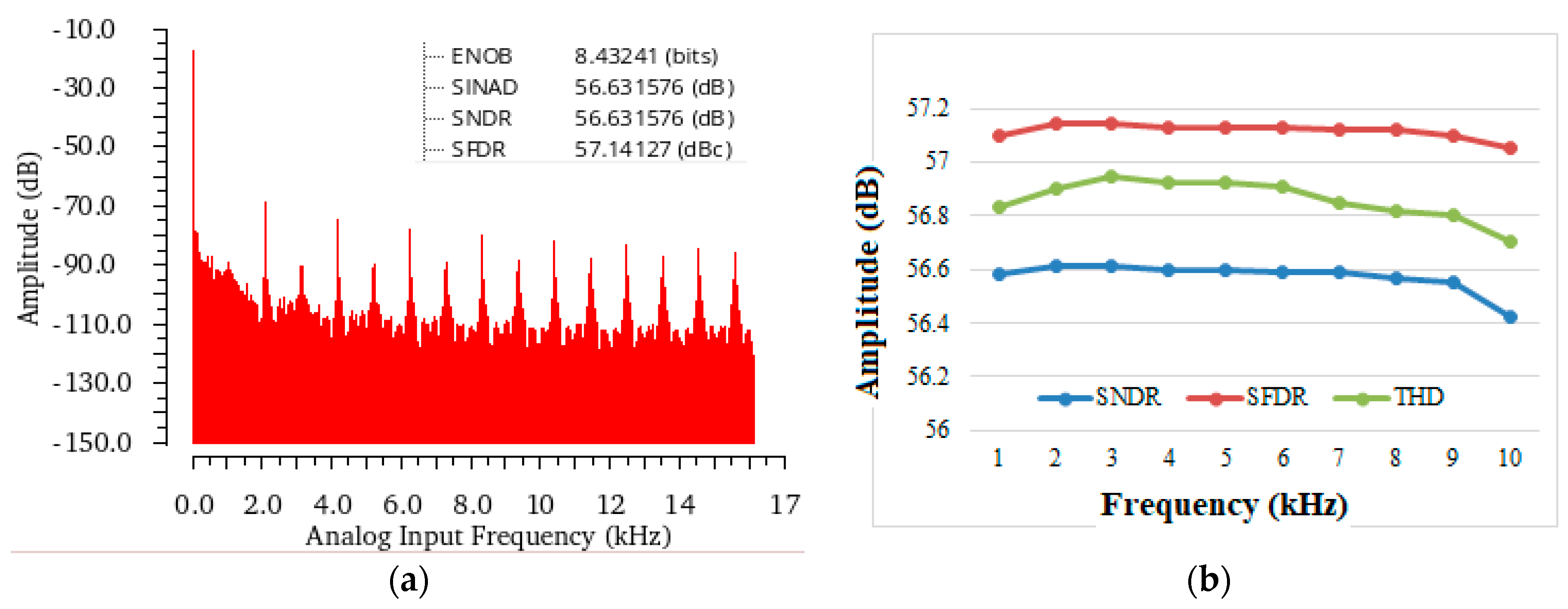
Figure 11.
Power breakdown.


Table 1.
Dimensions of each transistor.
| Mp1 | Mp2, Mp3 | Mn2, Mn3 | Mn4, Mn5 | Mn1 | |
|---|---|---|---|---|---|
| W (nm) | 120 | 240 | 120 | 1000 | 120 |
| L (nm) | 45 | 45 | 45 | 45 | 45 |
Table 2.
Comparative analysis.
| S. No. | [33] | [21] | [32] | [31] | Proposed |
|---|---|---|---|---|---|
| Technology (nm) | 45 | 45 | 45 | 45 | 45 |
| Supply Voltage (V) | 0.4 | 0.4 | 0.4 | 0.4 | 0.4 |
| No. of Transistors | 12 | 17 | 13 | 23 | 8 |
| Offset Voltage (mV) | 35.6 | 25 | 43 | 42 | 20 |
| Kickback Noise (mV) | 3.37 | 2.99 | 2.5 | 1.3 | 2 |
| Power (nW) | 6.77 | 4.6 | 1.97 | 10 | 1.07 |
| Leakage power (W) | 384 p | 1.33 n | 1.04 n | 33.2 p | 51.4 p |
| Delay (ns) | 15.14 | 6.75 | 5.15 | 15 | 7.16 |
Table 3.
2-Bit thermometer decoding truth table [13].
Table 3.
2-Bit thermometer decoding truth table [13].
| Binary Code | Thermometer Code | |||
|---|---|---|---|---|
| D2 | D1 | T3 | T2 | T1 |
| 0 | 0 | 0 | 0 | 0 |
| 0 | 1 | 0 | 0 | 1 |
| 1 | 0 | 0 | 1 | 1 |
| 1 | 1 | 1 | 1 | 1 |
Table 4.
2-Bit thermometer decoding truth table.
| Binary Code | New Code | |||
|---|---|---|---|---|
| D2 | D1 | C3 | C2 | C1 |
| 0 | 0 | 0 | 0 | 0 |
| 0 | 1 | 1 | 0 | 0 |
| 1 | 0 | 0 | 1 | 1 |
| 1 | 1 | 1 | 1 | 1 |
Table 5.
Comparison of leakage power of the bit-slice unit.
| Reference | Leakage Power (pW) |
|---|---|
| [36] | 56.08 |
| [37] | 41.8 |
| Modified | 38.4 |
Table 6.
Performance summary of the proposed ADC.
| Technology | 45 nm |
| Power Supply | 0.4 V |
| Reference Voltage | 0.2 V |
| DAC Size | 620 fF |
| SAR logic complexity | 271 transistors |
| Unit Capacitor | 20 fF |
| Input Range | [0, 0.4] V |
| DNL | −0.10/+0.13 LSB |
| INL | −0.8/+0.5 LSB |
| ENOB | 8.43 bits @ 2 kS/s |
| SNDR | 56.63 dB |
| SFDR | 57.14 dB |
| Power | 5.29 nW |
| Leakage Power | 1.5 nW |
| FOM | 7.66 fJ/conv.step @ 2 kS/s |
Table 7.
Performance summaries and comparison.
| [25] 2016 | [27] 2015 | [28] 2019 | [29] 2006 | [30] 2012 | [33] 2010 | [31] 2020 | [38] 2022 | Proposed | |
|---|---|---|---|---|---|---|---|---|---|
| Technology (nm) | 180 | 90 | 40 | 40 | 180 | 65 | 180 | 180 | 45 |
| Result | Sim. | Sim. | Fab. | Fab. | Fab. | Fab. | Fab. | Sim. | Sim. |
| Resolution (bit) | 9 | 9 | 9 | 9 | 8 | 10 | 8 | 10 | 9 |
| Supply (V) | 0.6 | 1 | 0.4 | 0.6 | 1.1 | 0.9 | 1 | 0.6 | 0.4 |
| Sampling Rate (kS/s) | 100 | 100 | 1 | 1 | 2 | 1 | 10 | 10 | 2 |
| Power (nW) | 399 | 473 | 1.8 | 130 | 27 | 5.8 | 90 | 41 | 5.29 |
| DNL (LSB) | - | +0.8/−0.6 | +0.36/−0.35 | +0.8/−0.65 | +0.28/−0.17 | +0.59/−0.62 | - | - | +0.13/−0.10 |
| INL (LSB) | - | +0.5/−0.7 | +0.44/−0.35 | +0.85/−0.6 | +0.81/−0.27 | +0.89/−0.41 | - | - | +0.5/−0.8 |
| SNDR (dB) | 53.5 | 53.55 | 50.1 | - | 46.3 | 56.5 | 65 | 61 | 56.63 |
| SFDR (dB) | 61.7 | 60.16 | 59.5 | - | 61.9 | 75.3 | 69 | 57.14 | |
| ENOB (bit) | 8.59 | 8.35 | 7.9 | 7.6 | 7.4 | 9.1 | 7 | 10 | 8.43 |
| FOM (fJ/conv.step) | 10.4 | 14.5 | 7.7 | 666 | 79.9 | 10.94 | 50 | 4.14 | 7.66 |
Disclaimer/Publisher’s Note: The statements, opinions and data contained in all publications are solely those of the individual author(s) and contributor(s) and not of MDPI and/or the editor(s). MDPI and/or the editor(s) disclaim responsibility for any injury to people or property resulting from any ideas, methods, instructions or products referred to in the content. |
© 2023 by the authors. Licensee MDPI, Basel, Switzerland. This article is an open access article distributed under the terms and conditions of the Creative Commons Attribution (CC BY) license (https://creativecommons.org/licenses/by/4.0/).
Share and Cite
MDPI and ACS Style
Lakshmi, P.V.; Musala, S.; Srinivasulu, A.; Ravariu, C. Design of a 0.4 V, 8.43 ENOB, 5.29 nW, 2 kS/s SAR ADC for Implantable Devices. Electronics 2023, 12, 4691. https://doi.org/10.3390/electronics12224691
AMA Style
Lakshmi PV, Musala S, Srinivasulu A, Ravariu C. Design of a 0.4 V, 8.43 ENOB, 5.29 nW, 2 kS/s SAR ADC for Implantable Devices. Electronics. 2023; 12(22):4691. https://doi.org/10.3390/electronics12224691
Chicago/Turabian StyleLakshmi, Posani Vijaya, Sarada Musala, Avireni Srinivasulu, and Cristian Ravariu. 2023. "Design of a 0.4 V, 8.43 ENOB, 5.29 nW, 2 kS/s SAR ADC for Implantable Devices" Electronics 12, no. 22: 4691. https://doi.org/10.3390/electronics12224691
Note that from the first issue of 2016, this journal uses article numbers instead of page numbers. See further details here.